Surface Roughness
At a microscopic scale no surface appears perfectly smooth. All materials exhibit surface irregularities and bumps. One measure of surface roughness is the root-mean-square (RMS) height h RMS of the surface bumps.
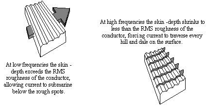
At low frequencies the depth of penetration of current (the skin depth) exceeds h RMS . Low-frequency currents therefore submarine below the surface bumps, unaffected by surface roughness.
High-frequency currents, on the other hand, remain tightly bound to the surface at all times. At frequencies so high that the skin depth d shrinks to less than h RMS , the current follows the contours of the surface, over hill and down dale, as it flows along the conductor. At these high frequencies the apparent resistance of the material increases to a value representative of the additional distance over which the current must flow to traverse the contours of the surface (Figure 2.23).
Figure 2.23. Surface roughness increases the apparent high-frequency resistance of a conductor

2.11.1 Severity of Surface Roughness
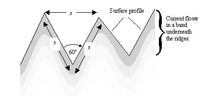
If the average incline of the conducting surface is 60 degrees (as if patterned with an infinite array of equilateral ridges perpendicular to the direction of current flow), the ultimate increase in surface resistance would be 100%. That's a pretty severe effect (Figure 2.24).
Figure 2.24. Current tightly bound to a series of equilateral ridges traverses distance 2 x for every distance x made good along the surface.

The exact dependence of skin-effect resistance on surface roughness defies analysis, as it depends not only on the height of the bumps, but also on their horizontal extent, spacing, and exact shape. Long, sinuous undulations don't cause much of a problem, whereas short, choppy, steep-faced bumps significantly increase the path length of the current. An infinite array of equilateral 3-D pyramids induces less of an effect than a series of equilateral ridges because, as anyone who hikes in the wilderness can tell you, you don't have to traverse every peak in order to make your way through the mountains .
Talk with your pcb vendor to explore the variety of surface treatments available that are compatible with your dielectric material.
2.11.2 Onset of Roughness Effect
The onset frequency for the RMS surface roughness effect depends on the square of the RMS surface roughness:
Equation 2.67

|
where |
m is the magnetic permeability (H/m), |
|
s is the conductivity (S/m) of the substrate, |
|
|
h RMS is the RMS bump height (m), and |
|
|
w rough is the frequency at which the roughness effect has assumed 60% of its ultimate effect (rad/s). |
|
|
For electro-deposited copper at room temperature m = 4 p ·10 “7 H/m and s = 5.98 ·10 7 S/m. |
|
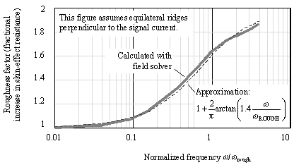
At the onset frequency the effective resistance of the conductor has progressed 60% of the way from the low-frequency asymptote (no effect) to the high-frequency asymptote (full effect). Figure 2.25 indicates the variation in roughness effect induced by an infinite array of equilateral ridges perpendicular to the direction of current flow. The equilateral ridges induce an ultimate effect of 100%, doubling the effective resistance of the material. Less severe geometries induce smaller ultimate effects, although probably with similar variations versus frequency.
Figure 2.25. At the onset frequency w rough the surface roughness has attained 60% of its ultimate effect (data taken from Harper, Electronic Packaging and Interconnection Handbook , 3rd ed., McGraw-Hill, 2000).

2.11.3 Roughness of Pcb Materials
Surface roughness plays an especially important role when working with pcb traces. This happens to a greater degree than with extruded conductors because pcb traces are often either chemically etched, leaving a naturally rough surface, or pressed onto rough substrate materials, leaving a mechanically imprinted pattern of roughness. Increased resistance in some cases as high as 10% to 50% above and beyond ordinary skin-effect considerations has been attributed to surface roughness.
The roughness of the copper layers used in pcb materials is often rated in terms of the average peak-to-valley height. The relation between peak-to-valley height and RMS roughness is not clear for practical materials. Taking the worst-case equilateral-ridge geometry as a guide, you might expect the RMS roughness to be on the order of 0.29 times the average peak-to-valley roughness.
Typical roughness treatments suitable for use with FR-4 dielectrics have been reported ranging from 6 to 18 m m (0.24 to 0.71 mil). Choosing the low end of this roughness range, and assuming an average peak-to-valley height of 6 m m corresponds to an RMS height of 1.7 m m (0.07 mil), the onset frequency works out to just over 1 GHz. Below 1 GHz you wouldn't notice the roughness effect; above it you would. Moving to a different material at the high end of the roughness range drops the onset frequency by a factor of nine, lowering it into the vicinity of a couple-of-hundred MHz.
2.11.4 Controlling Roughness
Vendors of pcb materials refer to the toothing profile of their cores when speaking about surface roughness. Toothing profiles are purposefully etched into the copper to facilitate adhesion between layers. Smoother materials exhibit less of a roughness effect [8] , [9] .
You may not have much choice about the surface treatment used on the inside surfaces of a core layer ”the core manufacturers make them pretty rough. What you can control are the surfaces on the outside of the core that are processed by your pcb fabricator. Stack your board so these are the heavy current-carrying surfaces on the bottom side (reference-plane- facing side) of your highest-frequency traces. That's where the current density is the highest and where surface roughness matters the most.
Pcb fabricators have access to many different surface treatments. The reverse-treat foil (RTF) process makes a surface that looks like the Himalayas. Sulfuric peroxide treatments add a dense forest of bushy trees to the Himalayas. The various oxide treatments (black, brown, and red oxide) produce cubic-looking crystalline shapes .
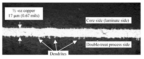
One of the most aggressive treatments, from the standpoint of good surface adhesion, is the double-treat process. It grows long, dendritic fingers that stick straight out from the copper surface, but leaves the underlying surface fairly smooth (Figure 2.26). Of all the choices, I like this best. My theory is that current on a double-treated surface will remain mostly bound to the smooth underlying surface, flowing like a river around the dendritic columns .
Figure 2.26. Dendritic fingers produced by the double-treat process stick up like dead trees (edge-view photomicrograph of 1/2-oz copper layer courtesy of Teradyne) .

Table 2.6 lists values for the surface roughness of copper as normally apply to various substrate materials [20] , [10] . Microwave designers often object to FR-4 materials because of their horrible loss tangent and the relatively rough surface treatments normally used to make the copper layers stick reliably to the dielectric material. For digital designs, however, surface roughness and dielectric losses don't render the material unusable ”they merely restrict the distances at which it can be used. In the table, the values given for roughness are the average peak-to-valley height, a number not easily translated into the RMS deviation needed for estimating the onset frequency. Taking the worst-case equilateral-ridge geometry as a guide, you might expect the RMS roughness to be on the order of 0.29 times the average peak-to-valley roughness.
POINTS TO REMEMBER
- At a microscopic level, all materials exhibit surface irregularities and bumps.
- Toothing profiles are purposefully etched into the copper to facilitate adhesion between layers.
- Roughness on a scale comparable to the skin depth increases the mean length of the path of current, increasing the resistance.
Table 2.6. Properties of pcb materials
|
Substrate |
Dielectric constant (1 MHz) |
Loss tan. |
Surface roughness (avg. peak-to-valley, m m) |
|---|---|---|---|
|
Air |
1.0005 |
||
|
Typical FR-4 applications |
4.5 |
0.01 “.025 |
6 “18 |
|
RT-duroid 5880 |
2.16 “2.24 |
0.0005- |
|
|
0.0015 |
0.75 “1.0 4.25-8.75 |
|
|
RT-duroid 6010 |
10.2 “10.7 |
0.001 “ |
|
|
0.006 |
0.75 “1.0 4.25-8.75 |
|
|
Alumina |
|||
|
10.1 9.6 8.5 |
0.0001 “2 0.0006 0.0015 |
0.05 “.25 5 “20 30 “50 |
|
Si (high resistivity) |
11.9 |
0.001 “ 0.01 |
0.025 |
|
GaAs |
12.85 |
0.0006 |
0.025 |
|
Single-crystal sapphire |
9.4, 11.6 (1) |
0.00004 “ 0.00007 |
0.005 “0.025 |
|
Fused quartz |
3.8 |
0.0001 |
0.006 “0.025 |
|
NOTE 1 ”Sapphire is an anisotropic dielectric material with different dielectric constants in two directions. NOTE 2 ”Some of the material in this chart has been adapted from [20] . |
|||
Fundamentals
- Impedance of Linear, Time-Invariant, Lumped-Element Circuits
- Power Ratios
- Rules of Scaling
- The Concept of Resonance
- Extra for Experts: Maximal Linear System Response to a Digital Input
Transmission Line Parameters
- Transmission Line Parameters
- Telegraphers Equations
- Derivation of Telegraphers Equations
- Ideal Transmission Line
- DC Resistance
- DC Conductance
- Skin Effect
- Skin-Effect Inductance
- Modeling Internal Impedance
- Concentric-Ring Skin-Effect Model
- Proximity Effect
- Surface Roughness
- Dielectric Effects
- Impedance in Series with the Return Path
- Slow-Wave Mode On-Chip
Performance Regions
- Performance Regions
- Signal Propagation Model
- Hierarchy of Regions
- Necessary Mathematics: Input Impedance and Transfer Function
- Lumped-Element Region
- RC Region
- LC Region (Constant-Loss Region)
- Skin-Effect Region
- Dielectric Loss Region
- Waveguide Dispersion Region
- Summary of Breakpoints Between Regions
- Equivalence Principle for Transmission Media
- Scaling Copper Transmission Media
- Scaling Multimode Fiber-Optic Cables
- Linear Equalization: Long Backplane Trace Example
- Adaptive Equalization: Accelerant Networks Transceiver
Frequency-Domain Modeling
- Frequency-Domain Modeling
- Going Nonlinear
- Approximations to the Fourier Transform
- Discrete Time Mapping
- Other Limitations of the FFT
- Normalizing the Output of an FFT Routine
- Useful Fourier Transform-Pairs
- Effect of Inadequate Sampling Rate
- Implementation of Frequency-Domain Simulation
- Embellishments
- Checking the Output of Your FFT Routine
Pcb (printed-circuit board) Traces
- Pcb (printed-circuit board) Traces
- Pcb Signal Propagation
- Limits to Attainable Distance
- Pcb Noise and Interference
- Pcb Connectors
- Modeling Vias
- The Future of On-Chip Interconnections
Differential Signaling
- Differential Signaling
- Single-Ended Circuits
- Two-Wire Circuits
- Differential Signaling
- Differential and Common-Mode Voltages and Currents
- Differential and Common-Mode Velocity
- Common-Mode Balance
- Common-Mode Range
- Differential to Common-Mode Conversion
- Differential Impedance
- Pcb Configurations
- Pcb Applications
- Intercabinet Applications
- LVDS Signaling
Generic Building-Cabling Standards
- Generic Building-Cabling Standards
- Generic Cabling Architecture
- SNR Budgeting
- Glossary of Cabling Terms
- Preferred Cable Combinations
- FAQ: Building-Cabling Practices
- Crossover Wiring
- Plenum-Rated Cables
- Laying Cables in an Uncooled Attic Space
- FAQ: Older Cable Types
100-Ohm Balanced Twisted-Pair Cabling
- 100-Ohm Balanced Twisted-Pair Cabling
- UTP Signal Propagation
- UTP Transmission Example: 10BASE-T
- UTP Noise and Interference
- UTP Connectors
- Issues with Screening
- Category-3 UTP at Elevated Temperature
150-Ohm STP-A Cabling
- 150-Ohm STP-A Cabling
- 150- W STP-A Signal Propagation
- 150- W STP-A Noise and Interference
- 150- W STP-A: Skew
- 150- W STP-A: Radiation and Safety
- 150- W STP-A: Comparison with UTP
- 150- W STP-A Connectors
Coaxial Cabling
- Coaxial Cabling
- Coaxial Signal Propagation
- Coaxial Cable Noise and Interference
- Coaxial Cable Connectors
Fiber-Optic Cabling
- Fiber-Optic Cabling
- Making Glass Fiber
- Finished Core Specifications
- Cabling the Fiber
- Wavelengths of Operation
- Multimode Glass Fiber-Optic Cabling
- Single-Mode Fiber-Optic Cabling
Clock Distribution
- Clock Distribution
- Extra Fries, Please
- Arithmetic of Clock Skew
- Clock Repeaters
- Stripline vs. Microstrip Delay
- Importance of Terminating Clock Lines
- Effect of Clock Receiver Thresholds
- Effect of Split Termination
- Intentional Delay Adjustments
- Driving Multiple Loads with Source Termination
- Daisy-Chain Clock Distribution
- The Jitters
- Power Supply Filtering for Clock Sources, Repeaters, and PLL Circuits
- Intentional Clock Modulation
- Reduced-Voltage Signaling
- Controlling Crosstalk on Clock Lines
- Reducing Emissions
Time-Domain Simulation Tools and Methods
- Ringing in a New Era
- Signal Integrity Simulation Process
- The Underlying Simulation Engine
- IBIS (I/O Buffer Information Specification)
- IBIS: History and Future Direction
- IBIS: Issues with Interpolation
- IBIS: Issues with SSO Noise
- Nature of EMC Work
- Power and Ground Resonance
Points to Remember
Appendix A. Building a Signal Integrity Department
Appendix B. Calculation of Loss Slope
Appendix C. Two-Port Analysis
- Appendix C. Two-Port Analysis
- Simple Cases Involving Transmission Lines
- Fully Configured Transmission Line
- Complicated Configurations
Appendix D. Accuracy of Pi Model
Appendix E. erf( )
Notes
EAN: N/A
Pages: 163
