Clock Distribution
The speed of computing has advanced prodigiously since the days of the ENIAC [99] , but the underlying architecture of the digital logic has not. Modern computers are still made from banks of synchronous logic regulated by a central clock. [112]
[112] The increasing trend towards the use of self-clocking data-communication links between chips may eventually obviate the need for board-level clock distribution. Such systems will, however, still maintain elaborate on-chip clock-distribution networks.
Clock signals display many unique characteristics. For example, most clocks toggle twice as fast as the data signals, making them the fastest signal within the system. The clock is also the most widely distributed signal within a digital machine. It connects to every flip-flop in a system, while individual data wires fan out to only a few devices each.
Because they are so fast, so heavily loaded, and so important for system timing, clock signals are subject to special requirements that may not apply to other signals.
Monotonic ” The clock is an asynchronous signal and therefore susceptible to double-clocking , or spurious clocking . To prevent these problems, the clock must be monotonic in the transition region (no glitches) and perfectly damped (no ringback into the transition region on either positive or negative edges).
Fast ” To minimizes lost timing margin due to the spread between V IL and V IH in most clock receivers, the clock signal must possess fast, square edges that rapidly proceed through the switching zone.
Low jitter ” The term clock jitter refers to instantaneous differences between the actual and ideal clock arrival times at any particular point. Clock jitter is caused by the superposition of other noisy signals onto the clock through various crosstalk mechanisms. To reduce jitter, you must reduce crosstalk.
High fan-out ” The clock feeds all the latches within a synchronous digital machine. It is distributed in a multilevel tree-like architecture to thousands (if not millions) of discrete locations.
Low skew ” Ideally, clock transitions should arrive synchronously at all points of usage within a digital system. Differences between the mean arrival times of the clock signals at different points within a system go by the name of clock skew . Most designers seek to minimize clock skew. In certain special cases, systems are designed with a specific amount of intentional clock skew.
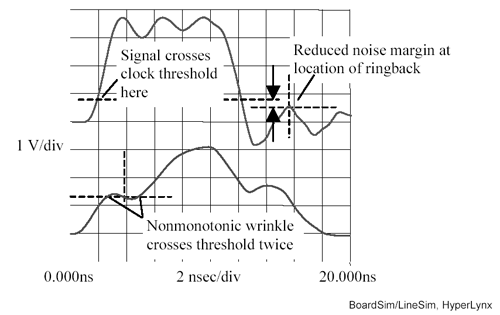
The monotonic requirement is identical to the requirement of first-incident wave switching on a data line. On the rising edge a clock signal must proceed quickly from V IL to V IH and stay there, with no lumps or ringback. On the falling edge it must transition cleanly from V IH to V IL . Wrinkles or pauses within the switching range between V IL and V IH must be avoided because such features greatly increase the likelihood of small noise events causing double-clocking (Figure 12.1). The requirement for monotonicity is met through a proper combination of line length, driver speed, and termination, just as it would be for any first-incident wave data signal. While data lines can tolerate a certain amount of nonmonotonic behavior or ringback as long as you don't sample the line at the instant these features occur, a clock receiver cannot tolerate such behavior at any time.
Figure 12.1. A poorly conditioned clock signal may cause double-clocking.

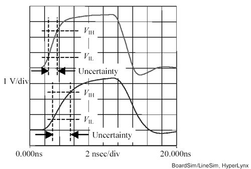
The requirement for fast switching speed is met by the selection of a sufficiently speedy clock driver. It doesn't help to pick a driver faster than the logic you are driving, as the clock receivers won't be able to respond to the faster risetime anyway, but you can damage your timing budget by picking a particularly slow-edged clock driver. Slow clock edges will render your system more susceptible to uncertainties in the clock receiver switching threshold and also more susceptible to crosstalk from external sources (Figure 12.2). The need for fast clock edges is one of the few signal-integrity requirements that are in diametric opposition to the needs of electromagnetic compatibility. Electromagnetic emissions are always improved by using a slower clock edge. Of course, electromagnetic emissions are also improved by using a slower clock frequency, but that's not usually practical.
Figure 12.2. A faster clock transition (top waveform) generates less uncertainty in the receiver switching moment.

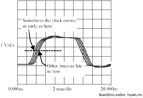
The jitter requirement becomes important when using your clock as a reference input for any kind of PLL circuit (Figure 12.3). To achieve low jitter, you must limit all forms of noise and crosstalk that impinge on the clock. Relevant sources of crosstalk may include other data traces on the same pcb, ground bounce within the clock driver package, and power supply noise that enters either the clock oscillator or any of its repeaters through their power terminals.
Figure 12.3. A jittery clock appears sometimes early and sometimes late.

The required fan-out may be obtained with any of the topologies discussed later in this chapter. In CMOS logic families fan-out is the most straightforward and easy to satisfy of the five requirements.
The last special issue for clocks is clock skew . For optimal system performance the clock transitions must arrive at all points precisely on time . The skew requirement constrains the tolerances on all terminations, line impedances, line delays, and load capacitances for every clock line. Let's look next at why clock skew is so important in high-speed architectures.
POINT TO REMEMBER
- Clock signals, because they are so fast, so heavily loaded, and so important for system timing, are subject to special requirements.
Fundamentals
- Impedance of Linear, Time-Invariant, Lumped-Element Circuits
- Power Ratios
- Rules of Scaling
- The Concept of Resonance
- Extra for Experts: Maximal Linear System Response to a Digital Input
Transmission Line Parameters
- Transmission Line Parameters
- Telegraphers Equations
- Derivation of Telegraphers Equations
- Ideal Transmission Line
- DC Resistance
- DC Conductance
- Skin Effect
- Skin-Effect Inductance
- Modeling Internal Impedance
- Concentric-Ring Skin-Effect Model
- Proximity Effect
- Surface Roughness
- Dielectric Effects
- Impedance in Series with the Return Path
- Slow-Wave Mode On-Chip
Performance Regions
- Performance Regions
- Signal Propagation Model
- Hierarchy of Regions
- Necessary Mathematics: Input Impedance and Transfer Function
- Lumped-Element Region
- RC Region
- LC Region (Constant-Loss Region)
- Skin-Effect Region
- Dielectric Loss Region
- Waveguide Dispersion Region
- Summary of Breakpoints Between Regions
- Equivalence Principle for Transmission Media
- Scaling Copper Transmission Media
- Scaling Multimode Fiber-Optic Cables
- Linear Equalization: Long Backplane Trace Example
- Adaptive Equalization: Accelerant Networks Transceiver
Frequency-Domain Modeling
- Frequency-Domain Modeling
- Going Nonlinear
- Approximations to the Fourier Transform
- Discrete Time Mapping
- Other Limitations of the FFT
- Normalizing the Output of an FFT Routine
- Useful Fourier Transform-Pairs
- Effect of Inadequate Sampling Rate
- Implementation of Frequency-Domain Simulation
- Embellishments
- Checking the Output of Your FFT Routine
Pcb (printed-circuit board) Traces
- Pcb (printed-circuit board) Traces
- Pcb Signal Propagation
- Limits to Attainable Distance
- Pcb Noise and Interference
- Pcb Connectors
- Modeling Vias
- The Future of On-Chip Interconnections
Differential Signaling
- Differential Signaling
- Single-Ended Circuits
- Two-Wire Circuits
- Differential Signaling
- Differential and Common-Mode Voltages and Currents
- Differential and Common-Mode Velocity
- Common-Mode Balance
- Common-Mode Range
- Differential to Common-Mode Conversion
- Differential Impedance
- Pcb Configurations
- Pcb Applications
- Intercabinet Applications
- LVDS Signaling
Generic Building-Cabling Standards
- Generic Building-Cabling Standards
- Generic Cabling Architecture
- SNR Budgeting
- Glossary of Cabling Terms
- Preferred Cable Combinations
- FAQ: Building-Cabling Practices
- Crossover Wiring
- Plenum-Rated Cables
- Laying Cables in an Uncooled Attic Space
- FAQ: Older Cable Types
100-Ohm Balanced Twisted-Pair Cabling
- 100-Ohm Balanced Twisted-Pair Cabling
- UTP Signal Propagation
- UTP Transmission Example: 10BASE-T
- UTP Noise and Interference
- UTP Connectors
- Issues with Screening
- Category-3 UTP at Elevated Temperature
150-Ohm STP-A Cabling
- 150-Ohm STP-A Cabling
- 150- W STP-A Signal Propagation
- 150- W STP-A Noise and Interference
- 150- W STP-A: Skew
- 150- W STP-A: Radiation and Safety
- 150- W STP-A: Comparison with UTP
- 150- W STP-A Connectors
Coaxial Cabling
- Coaxial Cabling
- Coaxial Signal Propagation
- Coaxial Cable Noise and Interference
- Coaxial Cable Connectors
Fiber-Optic Cabling
- Fiber-Optic Cabling
- Making Glass Fiber
- Finished Core Specifications
- Cabling the Fiber
- Wavelengths of Operation
- Multimode Glass Fiber-Optic Cabling
- Single-Mode Fiber-Optic Cabling
Clock Distribution
- Clock Distribution
- Extra Fries, Please
- Arithmetic of Clock Skew
- Clock Repeaters
- Stripline vs. Microstrip Delay
- Importance of Terminating Clock Lines
- Effect of Clock Receiver Thresholds
- Effect of Split Termination
- Intentional Delay Adjustments
- Driving Multiple Loads with Source Termination
- Daisy-Chain Clock Distribution
- The Jitters
- Power Supply Filtering for Clock Sources, Repeaters, and PLL Circuits
- Intentional Clock Modulation
- Reduced-Voltage Signaling
- Controlling Crosstalk on Clock Lines
- Reducing Emissions
Time-Domain Simulation Tools and Methods
- Ringing in a New Era
- Signal Integrity Simulation Process
- The Underlying Simulation Engine
- IBIS (I/O Buffer Information Specification)
- IBIS: History and Future Direction
- IBIS: Issues with Interpolation
- IBIS: Issues with SSO Noise
- Nature of EMC Work
- Power and Ground Resonance
Points to Remember
Appendix A. Building a Signal Integrity Department
Appendix B. Calculation of Loss Slope
Appendix C. Two-Port Analysis
- Appendix C. Two-Port Analysis
- Simple Cases Involving Transmission Lines
- Fully Configured Transmission Line
- Complicated Configurations
Appendix D. Accuracy of Pi Model
Appendix E. erf( )
Notes
EAN: N/A
Pages: 163
