IBIS: Issues with SSO Noise
IBIS Issues with SSO Noise
A powerful logic driver, when it switches from one state to another, draws a huge surge of current through its power pins. Some of this current is due to overlap in the ON conditions of the two transistors in a totem-pole driver circuit. This overlap current flows from V CC straight through to GND.
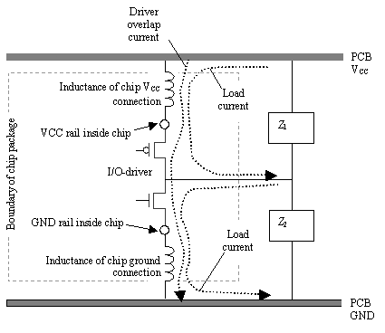
In addition to the overlap current, any current flowing to or from the load must also traverse the power pins (see Figure 13.8). When pulling low, current surges from the load, through the I/O pin, through the low-side FET, and from there flushes out the ground pin of the package back to the ground plane on the pcb and back to the load. When sourcing logic high, current surges from the power rail, through the power pin of the package, through the high-side FET, and from there through the I/O pin to the load. The point is, whatever current traverses an I/O pin must also somehow pass through the power or ground pins of the package.
Figure 13.8. Current surging through the I/O pin of the device must also traverse the power and ground connections, creating noise on the internal power and ground rails as it passes .
As current surges through the finite inductance of the chip's power and ground connections (the lead inductance of the package), it perturbs the voltage between the true ground plane on the pcb and the chip's internal ground substrate (or between the true power plane on the pcb and the chip's internal power net). These voltages are called simultaneous switching output noise (SSO noise) [101] , [102] . On the ground rail inside the chip, the magnitude of the SSO noise equals
Equation 13.2

|
where |
v SSO is the noise voltage on the ground substrate inside the chip package, |
|
i GROUND is the current flowing through the ground pins of the chip package, and |
|
|
L GROUND is the effective inductance of the array of ground pins. |
Equation [13.2] indicates that an SSO simulator needs to know (a) the effective cumulative inductance of all the ground pins in the package, and (b) the rate of change of current flowing through the ground pins. So far, so good. Here's the problem:
Item (a) can be measured in a variety of ways, but often the measured results are not available. Without this crucial piece of information, you can't make ground-bounce calculations. In this author's opinion, information about ground-pin inductance should be provided as a matter of routine by all package vendors . What I specifically want is a complete matrix of pin inductances and mutual pin inductances for the chip package. From this information, anyone can compute the effective inductance of any combination of ground pins (or power pins). There are optional provisions made in IBIS for incorporating such packaging information, and I wish everyone would provide the data .
Item (b) may be approximated if one knows the core currents required by the chip and also the sum of all I/O currents being drawn low by the output drivers. The conventional approach to computing this quantity is to first neglect the core currents on the assumption that the core currents are small compared to the massive I/O currents surging through the power and ground pins (a reasonable assumption for any but the largest VLSI circuits). Then use a ringing simulator to calculate the output current waveform for each output. From the output current waveforms, the peak di / dt due to each individual output may be estimated. The worst-case sum of all peak di / dt values may then be used for item (b), provided that the output currents sum linearly. The problem is, they don't. The drivers interact.
The driver interaction is caused by the shared power rails, which are bussed among I/O cells . When one output switches, it reduces the on-chip supply voltage available to the other drivers. When a driver is faced with a reduced power voltage, it switches more slowly than one with a full power voltage available. Therefore, when the second driver switches, the net maximum di / dt from the pair is less than twice the di / dt from a single driver. In other words, the assumption of independence used by IBIS simulators overestimates ground bounce, sometimes dramatically.
You can get a feeling for the sensitivity of a driver to ground bounce by simply operating the chip at a reduced DC power supply voltage. As you reduce the voltage, the output switching time usually slows down.
The IBIS committee has investigated the possibility of improving its specification file to incorporate the driver-to-driver interactions necessary to properly compute SSO noise, but to date has chosen not to do so.
POINT TO REMEMBER
- IBIS simulators don't yet properly compute SSO noise.
Fundamentals
- Impedance of Linear, Time-Invariant, Lumped-Element Circuits
- Power Ratios
- Rules of Scaling
- The Concept of Resonance
- Extra for Experts: Maximal Linear System Response to a Digital Input
Transmission Line Parameters
- Transmission Line Parameters
- Telegraphers Equations
- Derivation of Telegraphers Equations
- Ideal Transmission Line
- DC Resistance
- DC Conductance
- Skin Effect
- Skin-Effect Inductance
- Modeling Internal Impedance
- Concentric-Ring Skin-Effect Model
- Proximity Effect
- Surface Roughness
- Dielectric Effects
- Impedance in Series with the Return Path
- Slow-Wave Mode On-Chip
Performance Regions
- Performance Regions
- Signal Propagation Model
- Hierarchy of Regions
- Necessary Mathematics: Input Impedance and Transfer Function
- Lumped-Element Region
- RC Region
- LC Region (Constant-Loss Region)
- Skin-Effect Region
- Dielectric Loss Region
- Waveguide Dispersion Region
- Summary of Breakpoints Between Regions
- Equivalence Principle for Transmission Media
- Scaling Copper Transmission Media
- Scaling Multimode Fiber-Optic Cables
- Linear Equalization: Long Backplane Trace Example
- Adaptive Equalization: Accelerant Networks Transceiver
Frequency-Domain Modeling
- Frequency-Domain Modeling
- Going Nonlinear
- Approximations to the Fourier Transform
- Discrete Time Mapping
- Other Limitations of the FFT
- Normalizing the Output of an FFT Routine
- Useful Fourier Transform-Pairs
- Effect of Inadequate Sampling Rate
- Implementation of Frequency-Domain Simulation
- Embellishments
- Checking the Output of Your FFT Routine
Pcb (printed-circuit board) Traces
- Pcb (printed-circuit board) Traces
- Pcb Signal Propagation
- Limits to Attainable Distance
- Pcb Noise and Interference
- Pcb Connectors
- Modeling Vias
- The Future of On-Chip Interconnections
Differential Signaling
- Differential Signaling
- Single-Ended Circuits
- Two-Wire Circuits
- Differential Signaling
- Differential and Common-Mode Voltages and Currents
- Differential and Common-Mode Velocity
- Common-Mode Balance
- Common-Mode Range
- Differential to Common-Mode Conversion
- Differential Impedance
- Pcb Configurations
- Pcb Applications
- Intercabinet Applications
- LVDS Signaling
Generic Building-Cabling Standards
- Generic Building-Cabling Standards
- Generic Cabling Architecture
- SNR Budgeting
- Glossary of Cabling Terms
- Preferred Cable Combinations
- FAQ: Building-Cabling Practices
- Crossover Wiring
- Plenum-Rated Cables
- Laying Cables in an Uncooled Attic Space
- FAQ: Older Cable Types
100-Ohm Balanced Twisted-Pair Cabling
- 100-Ohm Balanced Twisted-Pair Cabling
- UTP Signal Propagation
- UTP Transmission Example: 10BASE-T
- UTP Noise and Interference
- UTP Connectors
- Issues with Screening
- Category-3 UTP at Elevated Temperature
150-Ohm STP-A Cabling
- 150-Ohm STP-A Cabling
- 150- W STP-A Signal Propagation
- 150- W STP-A Noise and Interference
- 150- W STP-A: Skew
- 150- W STP-A: Radiation and Safety
- 150- W STP-A: Comparison with UTP
- 150- W STP-A Connectors
Coaxial Cabling
- Coaxial Cabling
- Coaxial Signal Propagation
- Coaxial Cable Noise and Interference
- Coaxial Cable Connectors
Fiber-Optic Cabling
- Fiber-Optic Cabling
- Making Glass Fiber
- Finished Core Specifications
- Cabling the Fiber
- Wavelengths of Operation
- Multimode Glass Fiber-Optic Cabling
- Single-Mode Fiber-Optic Cabling
Clock Distribution
- Clock Distribution
- Extra Fries, Please
- Arithmetic of Clock Skew
- Clock Repeaters
- Stripline vs. Microstrip Delay
- Importance of Terminating Clock Lines
- Effect of Clock Receiver Thresholds
- Effect of Split Termination
- Intentional Delay Adjustments
- Driving Multiple Loads with Source Termination
- Daisy-Chain Clock Distribution
- The Jitters
- Power Supply Filtering for Clock Sources, Repeaters, and PLL Circuits
- Intentional Clock Modulation
- Reduced-Voltage Signaling
- Controlling Crosstalk on Clock Lines
- Reducing Emissions
Time-Domain Simulation Tools and Methods
- Ringing in a New Era
- Signal Integrity Simulation Process
- The Underlying Simulation Engine
- IBIS (I/O Buffer Information Specification)
- IBIS: History and Future Direction
- IBIS: Issues with Interpolation
- IBIS: Issues with SSO Noise
- Nature of EMC Work
- Power and Ground Resonance
Points to Remember
Appendix A. Building a Signal Integrity Department
Appendix B. Calculation of Loss Slope
Appendix C. Two-Port Analysis
- Appendix C. Two-Port Analysis
- Simple Cases Involving Transmission Lines
- Fully Configured Transmission Line
- Complicated Configurations
Appendix D. Accuracy of Pi Model
Appendix E. erf( )
Notes
EAN: N/A
Pages: 163
