Effect of Split Termination
A resistive load attenuates the output of a digital driver, but does not change its rise (or fall) time. Figure 12.21 illustrates this point with a basic step-response test. A digital logic gate is represented in the figure by a step voltage source with an output impedance of 10 W . The response y ( t ) is shown for four different values of R L .
Figure 12.21. A resistive load leaves t 10-90% unchanged,
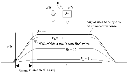
With R L set to infinity (an open circuit) the output y ( t ) duplicates x ( t ), rising to a full open-circuit voltage of the driver. Both 10% and 90% crossings are marked on the chart, illustrating the 10% to 90% open-circuit risetime of the source, t 10-90% .
With R L set to 100 ohms the signal does not rise quite so high. With a driver of 10 W and a load R L of 100 W , you should expect to see only a 90% response. [116] The signal at its peak will therefore only just approach 90% of the open-circuit amplitude. If you define risetime by waiting to see when the signal crosses 90% of the open-circuit voltage, you could be stuck waiting for a very long time indeed. With an 89- W load, for example, you'd never make it ”the risetime would be undefined.
[116] The exact amplitude should be 100/(100 + 10) times the open-circuit amplitude.
To avoid such difficulties, the risetime of a digital signal is defined as the difference between the times at which the signal crosses 10% and 90% of its own steady-state amplitude . With this definition, the 10% and 90% crossings of the 100- W loaded waveform line up exactly with the 10% and 90% points on the open-circuit waveform.
Load the circuit with 10 W and it cuts the signal in half, yet the 10% and 90% crossings of the half- sized signal line up exactly with the other signals. A 1- W load produces a very small signal indeed, but with the same 10% to 90% risetime as in the other cases.
Resistive loads make the signal smaller but do not change how quickly it moves from one level to another.
What confuses many engineers about this subject is the way resistive loading changes circuit timing. This effect is illustrated in Figure 12.22. Here the signal y ( t ) feeds a digital receiver, which has a fixed switching threshold. As the resistive load R L is changed, the threshold remains fixed, thereby changing the point in time at which the loaded waveform crosses the receiver threshold.
Figure 12.22. A resistive load pulling to ground retards the leading edge but accelerates the falling edge. Resistive loads pulling to V CC have the opposite effect.
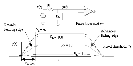
In this example a load of 10 W to ground retards the switching time associated with the rising edge, but advances the switching time associated with the falling edge. A 10- W resistor to V CC would have the opposite effect. Resistive loads have a definite effect on signal timing, but they do not change the 10% to 90% rise or fall time (or the signal bandwidth).
A split termination can provide an interesting timing adjustment. A split terminator acts in many ways just like a single resistor going to an adjustable battery. The setting of the battery is determined by the ratio R 1 / R 2 . This circuit (Figure 12.23) is called a Thevenin-equivalent circuit for the split termination.
Figure 12.23. Changing the ratio R 1 / R 2 biases a digital signal up or down by a small amount.
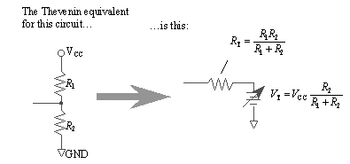
The Thevenin-equivalent battery voltage may be adjusted up or down by changing the ratio of R 1 / R 2 . The effect of this adjustment is to bias the DC level of digital signal y ( t ) up or down by a small amount. The degree of adjustment obtained depends on the ratio of the termination impedance (parallel combination of R 1 and R 2 ) as compared to the output resistance of the driver.
This DC-bias adjustment is normally made to ensure that the transmitting gate meets its V OH and V OL obligations; however, the same adjustment also is occasionally useful when making very small tweaks to system timing.
POINT TO REMEMBER
- Resistive loading attenuates the output of a digital driver, but does not change its rise (or fall) time.
Fundamentals
- Impedance of Linear, Time-Invariant, Lumped-Element Circuits
- Power Ratios
- Rules of Scaling
- The Concept of Resonance
- Extra for Experts: Maximal Linear System Response to a Digital Input
Transmission Line Parameters
- Transmission Line Parameters
- Telegraphers Equations
- Derivation of Telegraphers Equations
- Ideal Transmission Line
- DC Resistance
- DC Conductance
- Skin Effect
- Skin-Effect Inductance
- Modeling Internal Impedance
- Concentric-Ring Skin-Effect Model
- Proximity Effect
- Surface Roughness
- Dielectric Effects
- Impedance in Series with the Return Path
- Slow-Wave Mode On-Chip
Performance Regions
- Performance Regions
- Signal Propagation Model
- Hierarchy of Regions
- Necessary Mathematics: Input Impedance and Transfer Function
- Lumped-Element Region
- RC Region
- LC Region (Constant-Loss Region)
- Skin-Effect Region
- Dielectric Loss Region
- Waveguide Dispersion Region
- Summary of Breakpoints Between Regions
- Equivalence Principle for Transmission Media
- Scaling Copper Transmission Media
- Scaling Multimode Fiber-Optic Cables
- Linear Equalization: Long Backplane Trace Example
- Adaptive Equalization: Accelerant Networks Transceiver
Frequency-Domain Modeling
- Frequency-Domain Modeling
- Going Nonlinear
- Approximations to the Fourier Transform
- Discrete Time Mapping
- Other Limitations of the FFT
- Normalizing the Output of an FFT Routine
- Useful Fourier Transform-Pairs
- Effect of Inadequate Sampling Rate
- Implementation of Frequency-Domain Simulation
- Embellishments
- Checking the Output of Your FFT Routine
Pcb (printed-circuit board) Traces
- Pcb (printed-circuit board) Traces
- Pcb Signal Propagation
- Limits to Attainable Distance
- Pcb Noise and Interference
- Pcb Connectors
- Modeling Vias
- The Future of On-Chip Interconnections
Differential Signaling
- Differential Signaling
- Single-Ended Circuits
- Two-Wire Circuits
- Differential Signaling
- Differential and Common-Mode Voltages and Currents
- Differential and Common-Mode Velocity
- Common-Mode Balance
- Common-Mode Range
- Differential to Common-Mode Conversion
- Differential Impedance
- Pcb Configurations
- Pcb Applications
- Intercabinet Applications
- LVDS Signaling
Generic Building-Cabling Standards
- Generic Building-Cabling Standards
- Generic Cabling Architecture
- SNR Budgeting
- Glossary of Cabling Terms
- Preferred Cable Combinations
- FAQ: Building-Cabling Practices
- Crossover Wiring
- Plenum-Rated Cables
- Laying Cables in an Uncooled Attic Space
- FAQ: Older Cable Types
100-Ohm Balanced Twisted-Pair Cabling
- 100-Ohm Balanced Twisted-Pair Cabling
- UTP Signal Propagation
- UTP Transmission Example: 10BASE-T
- UTP Noise and Interference
- UTP Connectors
- Issues with Screening
- Category-3 UTP at Elevated Temperature
150-Ohm STP-A Cabling
- 150-Ohm STP-A Cabling
- 150- W STP-A Signal Propagation
- 150- W STP-A Noise and Interference
- 150- W STP-A: Skew
- 150- W STP-A: Radiation and Safety
- 150- W STP-A: Comparison with UTP
- 150- W STP-A Connectors
Coaxial Cabling
- Coaxial Cabling
- Coaxial Signal Propagation
- Coaxial Cable Noise and Interference
- Coaxial Cable Connectors
Fiber-Optic Cabling
- Fiber-Optic Cabling
- Making Glass Fiber
- Finished Core Specifications
- Cabling the Fiber
- Wavelengths of Operation
- Multimode Glass Fiber-Optic Cabling
- Single-Mode Fiber-Optic Cabling
Clock Distribution
- Clock Distribution
- Extra Fries, Please
- Arithmetic of Clock Skew
- Clock Repeaters
- Stripline vs. Microstrip Delay
- Importance of Terminating Clock Lines
- Effect of Clock Receiver Thresholds
- Effect of Split Termination
- Intentional Delay Adjustments
- Driving Multiple Loads with Source Termination
- Daisy-Chain Clock Distribution
- The Jitters
- Power Supply Filtering for Clock Sources, Repeaters, and PLL Circuits
- Intentional Clock Modulation
- Reduced-Voltage Signaling
- Controlling Crosstalk on Clock Lines
- Reducing Emissions
Time-Domain Simulation Tools and Methods
- Ringing in a New Era
- Signal Integrity Simulation Process
- The Underlying Simulation Engine
- IBIS (I/O Buffer Information Specification)
- IBIS: History and Future Direction
- IBIS: Issues with Interpolation
- IBIS: Issues with SSO Noise
- Nature of EMC Work
- Power and Ground Resonance
Points to Remember
Appendix A. Building a Signal Integrity Department
Appendix B. Calculation of Loss Slope
Appendix C. Two-Port Analysis
- Appendix C. Two-Port Analysis
- Simple Cases Involving Transmission Lines
- Fully Configured Transmission Line
- Complicated Configurations
Appendix D. Accuracy of Pi Model
Appendix E. erf( )
Notes
EAN: N/A
Pages: 163
