Arithmetic of Clock Skew
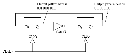
The circuit in Figure 12.5 is a two-bit ring counter , also called a switch-tail counter . When clocked at low speeds, the bit pattern at Q 1 repeats forever (...00110011...).
Figure 12.5. This two-bit ring counter fails at high frequencies due to a lack of setup time at D 2 .

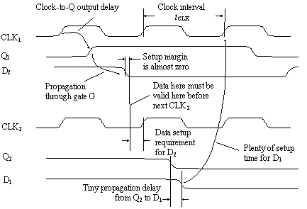
As you raise the clock frequency in Figure 12.5, the circuit continues to emit the same pattern until at some high frequency the circuit fails. The circuit fails because of a lack of setup time for flip-flop 2. At the failure frequency, the transitions at Q 1 emerge from gate G too late to meet the setup time requirement of D 2 . Figure 12.6 diagrams this failure mode. When clocked at or beyond the failure frequency, the circuit no longer produces an 0011 output sequence. This type of failure I call a setup-margin failure .
Figure 12.6. The setup time for D 2 dwindles to zero at high frequencies.

In the parlance of some timing-verification tools, a setup margin failure may also be called a setup-time violation , a critical- path failure , or a long-path failure . Automated timing-verification tools uncover such failures by computing a max-delay analysis in which they assume a worst-case maximum delay through every data propagation pathway and check that the data arrives at each D input sufficiently in advance of the next clock.
Note that setup-time violations happen at (and above) some particular clock frequency. Slowing down the clock fixes setup problems. Speeding up the clock causes them. This behavior is in contrast to the other form of timing difficulty, the hold-time violation .
In popular parlance a hold-time violation may also be called a short-path failure or a min-delay failure . An automated min-delay analysis assumes a worst-case minimum delay through every data propagation pathway and then checks that the data remains valid at each D input sufficiently long after each clock edge to satisfy the receiving flip-flop's hold-time requirement.
In an ordinary synchronous state machine with only one clock phase a setup-time violation involves one clock that produces a data transition and a second clock that receives it. This type of violation therefore heavily depends upon the clock interval. A hold-time violation, on the other hand, involves only a single clock edge that simultaneously changes the data at the output of one flip-flop while the next stage tries to latch the previous value of data before it changes. A hold-time violation is not affected by the clock interval. Slowing down the clock will not fix a hold-time problem.
The setup margin is defined in this circuit as the amount of time remaining between
- The time when signals actually emerge from gate G and
- The time when signals at D 2 must be valid to meet the setup requirement of flip-flop 2.
Setup margin measures the slack , or excess time, remaining in each clock cycle. A system with a big setup margin on every circuit can usually run at a higher clock speed without error.
As the clock speed in Figure 12.5 approaches its failure frequency, the setup margin drops to zero. Never operate a circuit near its failure frequency. Always de-rate the maximum operating speed for any circuit, leaving a small positive setup margin under all operating conditions. A positive setup margin protects your circuit against signal crosstalk that may slightly perturb the edge transition times, general miscalculations that often occur when counting logic delays, slightly out-of-spec gate delays, and later minor changes in the board design or layout.
A reasonable rule of thumb is to aim for a positive setup margin equal to about one gate delay. This rule of thumb allots more setup margin when working with slow logic families than with fast ones, keeping the setup margin fixed as a percentage of clock period over a wide range of designs. You will have to decide for yourself how much excess setup margin is acceptable.
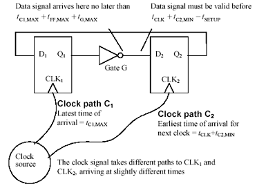
As drawn in Figure 12.5, the clock is assumed to arrive simultaneously at both clock inputs. Therefore, the only parameter of the clock that appears in the timing margin calculation is the clock interval. Figure 12.7 is a little more realistic. In this figure the clock arrives at each input with a slightly different delay, as it would in a real digital machine.
Figure 12.7. Any data edge arriving at D 2 must precede CLK 2 by amount t SETUP .

Figure 12.7 calculates the latest possible time of arrival for pulses emerging from gate G, comparing that to the earliest possible arrival time required by the setup conditions of flip-flop 2.
The latest possible arrival time for a pulse coming through gate G ( assuming the first clock occurs at time zero, and using the maximum delay times for all elements) is
Equation 12.1

|
where |
t SLOW is the slowest possible arrival time for pulse from gate G, s, |
|
t C1,MAX is the maximum delay of path C 1 , s, |
|
|
t FF,MAX is the maximum delay, clock to Q, of flip-flop 1, s, and |
|
|
t G,MAX is the maximum delay of gate G, including circuit trace delay, s. |
The pulse from G will be clocked into flip-flop 2 on the next clock pulse. This clock edge is produced by the clock source at time zero plus t CLK , but then it must propagate through path C 2 to input CLK 2 . The earliest possible arrival for the next clock at CLK 2 is therefore t CLK + t C2,MIN . Flip-flop 2 requires a valid input at least t SETUP before the arrival of the next clock at CLK 2 , leading to this equation for the time at which the signal from gate G is required.
Equation 12.2

|
where |
t REQUIRED = time by which data from G must arrive, s, |
|
t CLK = interval between clocks, s, |
|
|
t C2,MIN = minimum delay of path C 2 , s, and |
|
|
t SETUP = worst-case setup time required by flip-flop 2, s. |
Equation [12.2] uses the minimum delay time for clock path C 2 , which moves the required data arrival time to the earliest possible (worst-case) condition.
If the data is to arrive in time for the system to function, time [12.1] must precede [12.2].
Equation 12.3

This constraint may be expanded using equations [12.1] and [12.2]:
Equation 12.4

In words, the clock interval must exceed the sum of the flip-flop delay, the gate delay, and the setup time, plus a timing correction for the delay of paths C 1 and C 2 . [113]
[113] Equation [12.4] represents only the setup-time constraint for the circuit in Figure 12.7. There is a second constraint related to the hold time required by D 2 .
The first three terms make perfect sense because all three events must occur in sequence each cycle. The timing correction for C 1 and C 2 is more subtle. It involves the difference in clock arrival times at nodes CLK 1 and CLK 2 . This difference is called clock skew . For example, if the clock arrives late at flip-flop 1, then output Q 1 also occurs late, deteriorating your timing margin. If at the same time delay C 2 happened to be unusually small, flip-flop 2 gets clocked earlier, requiring that the data be valid that much earlier than usual. This also deteriorates your timing margin. In either case you must expand the clock period, slowing down system performance, to fix the problem. Clock skew directly affects your timing margins and thus the maximum speed at which a system may be operated.
Automated maximum-delay analysis routines have to be smart enough to understand the impact of skew on timing analysis. These routines must not only maximize the delay through all data paths, but also maximize the clock distribution delay to the source register while minimizing the clock distribution delay to the destination register. Alternately, you may assume during analysis that the clock arrives coincident everywhere and then insist that the calculated setup margin exceed the maximum absolute amount of clock skew you anticipate in your system.
What if CLK 2 arrives late instead of early? If it is not so late that it causes a hold-time violation at D 2 , a delayed CLK 2 can actually improve the maximum operating speed of the system. This works because delaying CLK 2 increases the setup margin at D 2 . Some designers make clever use of this effect, carefully adjusting the clock at each stage for maximum performance.
Delaying CLK 2 improves performance only when you are fighting a setup-time problem (a long-path problem). If your circuit has a hold-time problem (a short-path problem) then you might try advancing CLK 2 , if possible, to improve the situation.
Intentional adjustments to the clock skew do not provide many benefits in circuits that have feedback from later stages back to the beginning, unless the feedback path happens to incorporate much less delay than the typical delay between the other stages. For example, retarding the clock on flip-flop 2 in Figure 12.7 adds timing margin to D 2 , but takes it away from D 1 . The system might run a little faster that way, but only to the extent that the delay through G is bigger than the wiring-delay from Q 2 back to D 1 . Most designers ignore these fine adjustments and just try to minimize clock skew so they don't have to worry explicitly about it.
Note that in equation [12.4] only the difference in clock propagation delays matters. The absolute amount of clock delay, as long as it is balanced between the two paths, does not matter.
In the practical world, a clock interval is usually crystal-controlled, and so there is very little uncertainty in the parameter t CLK . If the clock oscillator is not crystal-controlled, its nominal frequency should be offset slightly to guarantee that the shortest possible clock interval always exceeds t CLK .
Equation [12.4] tells us that clock skew has as much of an impact on overall operating speed as the propagation delay of any other signal. As a result, rather than spend their time optimizing the delay of every data net in a big design, many engineers choose instead to concentrate their efforts on minimizing clock skew. In a resource-constrained design environment, this is a sound strategy.
EXAMPLE Calculation of System Timing Budget
Here is a system-level timing budget for a hypothetical system constructed with bipolar logic. The budget provides for two sections of logic (10EP58 MUX chips) between each stage of flip-flops (10EP31). A common clock is distributed through a multiple-output low-skew clock driver (10EP14) to each flip-flop clock input. All times are in picoseconds. [114]
[114] The specifications of any logic family are subject to change at any time.
|
Flip-flop |
10EP31 clk |
475 |
||
|
Setup time |
150 |
|||
|
Subtotal |
625 |
|||
|
Combinatorial logic |
10EP58 MUX |
400 |
||
|
pcb trace 25 mm |
180 |
|||
|
x two sections |
x2 |
|||
|
Subtotal |
1160 |
|||
|
Clock skew |
Max-min per gate 10EP14 |
50 |
||
|
pcb trace skew 2.5 mm |
18 |
|||
|
Subtotal |
68 |
|||
|
Timing margin |
7.3% of clock period |
147 |
||
|
Total budget |
2000 |
|||
|
Clock period |
500 MHz |
2000 |
POINTS TO REMEMBER
- Timing margin measures the slack, or excess time, remaining in each clock cycle.
- Lowering the clock frequency fixes setup problems, but not hold problems.
- Clock skew affects operating speed as much as any other propagation delay.
Fundamentals
- Impedance of Linear, Time-Invariant, Lumped-Element Circuits
- Power Ratios
- Rules of Scaling
- The Concept of Resonance
- Extra for Experts: Maximal Linear System Response to a Digital Input
Transmission Line Parameters
- Transmission Line Parameters
- Telegraphers Equations
- Derivation of Telegraphers Equations
- Ideal Transmission Line
- DC Resistance
- DC Conductance
- Skin Effect
- Skin-Effect Inductance
- Modeling Internal Impedance
- Concentric-Ring Skin-Effect Model
- Proximity Effect
- Surface Roughness
- Dielectric Effects
- Impedance in Series with the Return Path
- Slow-Wave Mode On-Chip
Performance Regions
- Performance Regions
- Signal Propagation Model
- Hierarchy of Regions
- Necessary Mathematics: Input Impedance and Transfer Function
- Lumped-Element Region
- RC Region
- LC Region (Constant-Loss Region)
- Skin-Effect Region
- Dielectric Loss Region
- Waveguide Dispersion Region
- Summary of Breakpoints Between Regions
- Equivalence Principle for Transmission Media
- Scaling Copper Transmission Media
- Scaling Multimode Fiber-Optic Cables
- Linear Equalization: Long Backplane Trace Example
- Adaptive Equalization: Accelerant Networks Transceiver
Frequency-Domain Modeling
- Frequency-Domain Modeling
- Going Nonlinear
- Approximations to the Fourier Transform
- Discrete Time Mapping
- Other Limitations of the FFT
- Normalizing the Output of an FFT Routine
- Useful Fourier Transform-Pairs
- Effect of Inadequate Sampling Rate
- Implementation of Frequency-Domain Simulation
- Embellishments
- Checking the Output of Your FFT Routine
Pcb (printed-circuit board) Traces
- Pcb (printed-circuit board) Traces
- Pcb Signal Propagation
- Limits to Attainable Distance
- Pcb Noise and Interference
- Pcb Connectors
- Modeling Vias
- The Future of On-Chip Interconnections
Differential Signaling
- Differential Signaling
- Single-Ended Circuits
- Two-Wire Circuits
- Differential Signaling
- Differential and Common-Mode Voltages and Currents
- Differential and Common-Mode Velocity
- Common-Mode Balance
- Common-Mode Range
- Differential to Common-Mode Conversion
- Differential Impedance
- Pcb Configurations
- Pcb Applications
- Intercabinet Applications
- LVDS Signaling
Generic Building-Cabling Standards
- Generic Building-Cabling Standards
- Generic Cabling Architecture
- SNR Budgeting
- Glossary of Cabling Terms
- Preferred Cable Combinations
- FAQ: Building-Cabling Practices
- Crossover Wiring
- Plenum-Rated Cables
- Laying Cables in an Uncooled Attic Space
- FAQ: Older Cable Types
100-Ohm Balanced Twisted-Pair Cabling
- 100-Ohm Balanced Twisted-Pair Cabling
- UTP Signal Propagation
- UTP Transmission Example: 10BASE-T
- UTP Noise and Interference
- UTP Connectors
- Issues with Screening
- Category-3 UTP at Elevated Temperature
150-Ohm STP-A Cabling
- 150-Ohm STP-A Cabling
- 150- W STP-A Signal Propagation
- 150- W STP-A Noise and Interference
- 150- W STP-A: Skew
- 150- W STP-A: Radiation and Safety
- 150- W STP-A: Comparison with UTP
- 150- W STP-A Connectors
Coaxial Cabling
- Coaxial Cabling
- Coaxial Signal Propagation
- Coaxial Cable Noise and Interference
- Coaxial Cable Connectors
Fiber-Optic Cabling
- Fiber-Optic Cabling
- Making Glass Fiber
- Finished Core Specifications
- Cabling the Fiber
- Wavelengths of Operation
- Multimode Glass Fiber-Optic Cabling
- Single-Mode Fiber-Optic Cabling
Clock Distribution
- Clock Distribution
- Extra Fries, Please
- Arithmetic of Clock Skew
- Clock Repeaters
- Stripline vs. Microstrip Delay
- Importance of Terminating Clock Lines
- Effect of Clock Receiver Thresholds
- Effect of Split Termination
- Intentional Delay Adjustments
- Driving Multiple Loads with Source Termination
- Daisy-Chain Clock Distribution
- The Jitters
- Power Supply Filtering for Clock Sources, Repeaters, and PLL Circuits
- Intentional Clock Modulation
- Reduced-Voltage Signaling
- Controlling Crosstalk on Clock Lines
- Reducing Emissions
Time-Domain Simulation Tools and Methods
- Ringing in a New Era
- Signal Integrity Simulation Process
- The Underlying Simulation Engine
- IBIS (I/O Buffer Information Specification)
- IBIS: History and Future Direction
- IBIS: Issues with Interpolation
- IBIS: Issues with SSO Noise
- Nature of EMC Work
- Power and Ground Resonance
Points to Remember
Appendix A. Building a Signal Integrity Department
Appendix B. Calculation of Loss Slope
Appendix C. Two-Port Analysis
- Appendix C. Two-Port Analysis
- Simple Cases Involving Transmission Lines
- Fully Configured Transmission Line
- Complicated Configurations
Appendix D. Accuracy of Pi Model
Appendix E. erf( )
Notes
EAN: N/A
Pages: 163
 Q
Q