Clock Repeaters
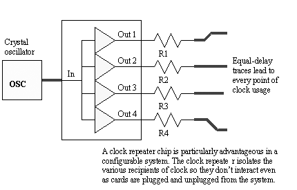
A clock repeater can distribute clock signals on an individual pcb or between the boards of a more complex system. A wide variety of repeater architectures is available. As shown in Figure 12.8, the typical clock repeater chip has one input pin but multiple output pins. The outputs are all ganged together, replicating multiple copies of the input signal. Each output is usually endowed with a large, powerful driver. These high- powered outputs may be used to construct extremely well- terminated transmission lines, a key element in the battle for monotonic, square-edged, and perfectly damped clock signals.
Figure 12.8. A clock repeater with one input and multiple outputs.
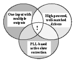
The variety of clock repeater chips is practically unlimited. Repeater chips are available in almost every conceivable logic family, with a varying number of outputs and a broad selection of ancillary features. What these chips have in common are three things: multiple outputs, low-impedance drivers, and low skew (Figure 12.9).
Figure 12.9. Clock driver chips can provide many combinations of features: multiple outputs, high-powered drivers, and active skew correction.
The existence of multiple outputs facilitates high fan-out. The potential number of outputs is limited in theory only by the packaging and by marketing considerations. In practice, most clock repeater chips provide between 4 and 20 outputs.
The low-impedance driver outputs are not intended to help you hook up multiple loads to each output. Rather, they are provided so that you can attach an accurate external series-terminating resistor to precisely match your transmission line impedance. The output impedance of the driver, if it is sufficiently low, will then have little bearing on the performance of the termination.
Clocks should always be terminated regardless of line length. This helps insure that your clock signals enjoy a predictable relation between line length and signal delay.
Table 12.1 lists the timing performance of a selected sample of clock repeater chips. For each chip, the table lists the output-to-output skew and also the part-to-part timing uncertainty. The output-to-output skew is the magnitude of the worst-case skew from any output to any other output under all allowed operating conditions. The part-to-part uncertainty is the worst-case skew that would prevail in an application like Figure 12.10, which apparently requires more outputs than are available from a single clock repeater. The part-to-part uncertainty matters only in architectures that chain clock repeaters together into a multilayer clock distribution tree. In small applications served by a single clock repeater chip the part-to-part uncertainty specification is irrelevant.
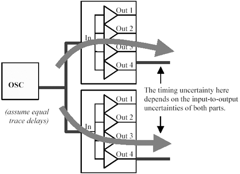
Figure 12.10. A sufficiently powerful oscillator can directly drive two or more proximate clock repeaters. The effectiveness of this approach is limited by the input-to-output timing uncertainty of the repeater chips.
Gallium-Arsenide and Bipolar chips show wonderfully skew; however, these parts also tend to be quite power-hungry. They may also provide in some cases non-TTL outputs which, if they must be translated to TTL levels before you can use the clock, will lose their wonderful low-skew properties as they pass through the translator.
Figure 12.10 illustrates one brute-force way to expand the number of low-skew outputs. If the oscillator output driver is sufficiently powerful, and if the clock repeater chips are located sufficiently close together, a single oscillator may directly drive multiple clock repeater inputs. If the oscillator cannot drive two loads, or if trace delay between the clock repeater inputs exceeds 1/6 of the clock risetime, the tree configuration shown in Figure 12.11 works better. In either case, any predictable delay through the clock repeaters is the same for both branches of the distribution and so has no impact on the delivered clock skew, but the input-to-output timing uncertainty affects the overall skew in a direct manner.
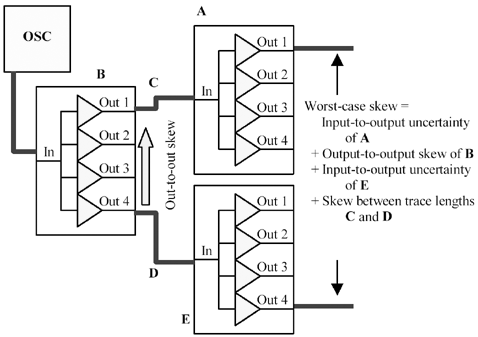
Figure 12.11. The performance of a tree structure depends heavily on the input-to-output uncertainty of the clock repeaters.
Beware that many clock repeaters, while they may have terrific output-to-output skew specifications, may not perform well in a chained application because of poor control over the input-to-output skew. Special considerations concerning chaining of clock repeaters appear in Section 12.3.1, "Active Skew Correction," and Section 12.3.2, "Zero-Delay Clock Repeaters."
Table 12.1. Specifications for Selected Clock Repeaters
|
Part |
Logic family |
Intended use |
Number of outputs |
Output-to-output skew ( ±ps) |
Part-to-part uncertainty ( ± ps) |
Min. risetime (ps) |
Max. operating frequency (MHz) |
|---|---|---|---|---|---|---|---|
|
Vitesse VSC6110 |
GaAs |
50- W diff. |
4 |
50 |
” |
” |
1250 |
|
AZ10E111 |
5V-ECL |
50- W diff. |
9 |
75 |
150 |
250 |
500 |
|
Fairchild 100310 |
5V-ECL |
50- W diff. |
8 |
50 |
400 |
275 |
750 |
|
AMCC S3LV308 |
BiCMOS |
65-75- W |
20 |
350 |
500 |
1500 |
100 |
|
IDT 5T907 |
2.5V CMOS |
±8 mA for short lines only |
10 |
25 |
300 |
” |
250 |
|
IDT CSPT857A |
2.5V CMOS PLL |
60- W diff. |
10 |
75 |
100 |
1000 |
200 |
|
Cypress CY2300 |
CMOS zero-delay buffer |
±8 mA for short lines only |
4 |
200 |
400 |
” |
66 |
Keeping the clock repeater isolated in its own package is a good idea. When you use an independent clock repeater chip, there is no possibility that the clock outputs will become corrupted with ground bounce from other circuits within the same package. If you use instead a few extra outputs from, say, a 512-pin ASIC chip to source your clock signals, those outputs may become corrupted with substantial amounts of simultaneous switching noise (ground bounce) coming from other I/O cells switching within the same package. With the clock repeater safely isolated in its own, separate, isolated package, ground-bounce isn't a problem. A separate clock repeater package also makes it easy to maintain a healthy physical separation from other noisy signals on the board, keeping the clocks free from crosstalk.
POINTS TO REMEMBER
- The performance of a clock tree structure depends heavily on the input-to-output uncertainty of the clock repeaters.
- Keeping the clock repeater isolated in its own package is a good idea.
12.3.1 Active Skew Correction
No manufacturer can accurately predetermine the delay of a CMOS driver; however, anyone can construct a circuit that measures differences in delay with great precision. This idea suggests the use of phase-locked -loop (PLL) or delay-locked-loop (DLL) technology to automatically compensate for the natural propagation delays internal to a clock repeater.
Figure 12.12 illustrates one way that DLL technology might be used to null the output-to-output skew of a clock repeater. In the figure, one of the outputs (Y1) is designated as the reference output. Some fixed (but unpredictable) delay is built into the reference output circuit. The circuit compares the timing of the Y2 output with the timing of the reference (at pin REF), and then adjusts the internal delay on the Y2 driver until the Y2 output matches perfectly with the reference, to within the tolerance limits of the phase comparator. All the other channels include a similar auto-adjustment feedback loop. The automatic skew compensation architecture in Figure 12.12 is a form of delay-locked loop .
Figure 12.12. In a skew-compensated clock repeater, each output is automatically adjusted to match the reference output.
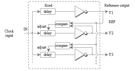
A skew-compensated structure delivers far better output-to-output skew than does a noncompensated structure, but does nothing to combat uncertainty in the overall input-to-output delay.
Beware that actively compensated repeaters, because they incorporate sensitive analog circuitry , are susceptible to power supply noise. Always follow the manufacturer's guidelines for power supply filtering and supply a clean, jitter-free reference clock.
POINTS TO REMEMBER
- A skew-compensated clock repeater architecture does nothing to combat uncertainty in the overall input-to-output delay.
- Actively compensated clock repeaters are highly susceptible to power supply noise.
12.3.2 Zero-Delay Clock Repeaters
If it's the input-to-output uncertainty you wish to improve, you will need a part that regulates its outputs in comparison not to each other, but to the input. Such a part is called a zero-delay clock buffer. It's the ultimate part for big clock tree applications.
A PLL-type zero-delay repeater incorporates an ordinary clock repeater, a phase detector, and a voltage-controlled oscillator, or VCO (Figure 12.13). The DLL-style zero-delay repeater substitutes an adjustable delay chain for the VCO. In either case, the components are hooked up such that the phase detector can adjust the VCO or the delay chain to cause the output transitions to line up directly on top of the input transitions.
Figure 12.13. The zero-delay clock repeater locks the reference output precisely to the reference input.
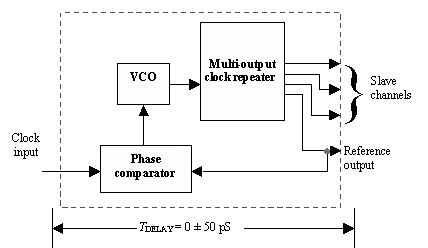
In a PLL-basead part, when first powered on, the phase comparator examines the frequency relationship between the input and output sections and works to slew the VCO into a rough frequency lock. From there, the phase comparator makes more delicate adjustments, eventually nudging the VCO into precise phase lock with the source. After a suitable warm-up period, the precise input-to-output delay should be very nearly zero. A DLL-based part undergoes a similar start-up sequence.
Beware that actively compensated repeaters, because they incorporate sensitive analog circuitry, are susceptible to power supply noise. Always follow the manufacturer's guidelines for power supply filtering and supply a clean, jitter-free reference clock.
Regarding the PLL versus DLL controversy, you will undoubtedly see many purported proofs of the inherent superiority of a DLL control loop as opposed to the PLL variety. It's commonly stated that a DLL, because it doesn't contain an oscillator, will produce less jitter and noise at its output. Such arguments are fallacious. While there may be certain architectural advantages to the DLL structure, the noise produced by all presently available integrated-chip PLL or DLL circuits is not dominated by subtle theoretical limitations of the system architecture. It is dominated by crosstalk from the power system, crosstalk from other circuits within the chip, and noise caused by switching between delay taps, operating charge pumps, and so forth within the circuit. The difference between parts is not the architecture, but the talent and experience of the designer who built the part. Focus your decision-making process on externally observable specifications, like worst-case skew and RMS jitter, and forget about whether it's a PLL or a DLL inside.
POINT TO REMEMBER
- A zero-delay clock buffer directly controls the input-to-output uncertainty.
12.3.3 Compensating for Line Length
Low-skew and zero-delay repeaters have as their goal the creation of multiple clock waveforms with low skew. The skew is defined at the output pins of the repeater chip. What you really want, however, is something a little different. What you really want is low skew as defined at the points of usage . To obtain the latter from the former, you are forced to provide equal-delay traces to every load, with the same terminations and loading on every trace.
Wouldn't it be grand if the clock repeater could just automatically measure the trace delays to every point of usage? What if it could automatically compensate for the individual time-of-flight on every trace? Such a part would free you from having to worry about the clock trace lengths.
At one time, there was such a part (Microlinear ML6510 ”see Figure 12.14). This component made use of a special property of series-terminated lines. The figure illustrates a clock driver at point A, an external series-terminating resistor leading to point B, and a remote clock receiver at point C. Assuming the line was perfectly terminated , there would appear two transitions at point B for every clock edge. Each transition was half- sized , and the spacing between transitions was precisely one transmission-line round-trip delay.
Figure 12.14. The reflections on a source-terminated circuit can be used to determine when each clock edge actually hits the far end.
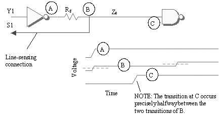
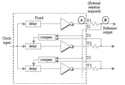
If point B was made accessible to the clock repeater chip (Figure 12.15), the chip would have gained all the information necessary to determine when the clock edges were actually reaching the end of each line. The clock repeater used two comparator circuits, one set to detect the first transition and the other set to detect the second transition, and then it averaged the two times to estimate the time-of-arrival for each clock edge. [115] The internal feedback loop then compensated the delay on each output such that the clocks were received at the correct times.
[115] Circuits designed to perform this feat are very similar to circuits used in data-transmission systems to position the clock edges midway between successive data transitions.
Figure 12.15. Each output requires two pins: a driver pin and a line-sensing pin.
POINT TO REMEMBER
- What you really want is low skew as defined at the points of usage .
Fundamentals
- Impedance of Linear, Time-Invariant, Lumped-Element Circuits
- Power Ratios
- Rules of Scaling
- The Concept of Resonance
- Extra for Experts: Maximal Linear System Response to a Digital Input
Transmission Line Parameters
- Transmission Line Parameters
- Telegraphers Equations
- Derivation of Telegraphers Equations
- Ideal Transmission Line
- DC Resistance
- DC Conductance
- Skin Effect
- Skin-Effect Inductance
- Modeling Internal Impedance
- Concentric-Ring Skin-Effect Model
- Proximity Effect
- Surface Roughness
- Dielectric Effects
- Impedance in Series with the Return Path
- Slow-Wave Mode On-Chip
Performance Regions
- Performance Regions
- Signal Propagation Model
- Hierarchy of Regions
- Necessary Mathematics: Input Impedance and Transfer Function
- Lumped-Element Region
- RC Region
- LC Region (Constant-Loss Region)
- Skin-Effect Region
- Dielectric Loss Region
- Waveguide Dispersion Region
- Summary of Breakpoints Between Regions
- Equivalence Principle for Transmission Media
- Scaling Copper Transmission Media
- Scaling Multimode Fiber-Optic Cables
- Linear Equalization: Long Backplane Trace Example
- Adaptive Equalization: Accelerant Networks Transceiver
Frequency-Domain Modeling
- Frequency-Domain Modeling
- Going Nonlinear
- Approximations to the Fourier Transform
- Discrete Time Mapping
- Other Limitations of the FFT
- Normalizing the Output of an FFT Routine
- Useful Fourier Transform-Pairs
- Effect of Inadequate Sampling Rate
- Implementation of Frequency-Domain Simulation
- Embellishments
- Checking the Output of Your FFT Routine
Pcb (printed-circuit board) Traces
- Pcb (printed-circuit board) Traces
- Pcb Signal Propagation
- Limits to Attainable Distance
- Pcb Noise and Interference
- Pcb Connectors
- Modeling Vias
- The Future of On-Chip Interconnections
Differential Signaling
- Differential Signaling
- Single-Ended Circuits
- Two-Wire Circuits
- Differential Signaling
- Differential and Common-Mode Voltages and Currents
- Differential and Common-Mode Velocity
- Common-Mode Balance
- Common-Mode Range
- Differential to Common-Mode Conversion
- Differential Impedance
- Pcb Configurations
- Pcb Applications
- Intercabinet Applications
- LVDS Signaling
Generic Building-Cabling Standards
- Generic Building-Cabling Standards
- Generic Cabling Architecture
- SNR Budgeting
- Glossary of Cabling Terms
- Preferred Cable Combinations
- FAQ: Building-Cabling Practices
- Crossover Wiring
- Plenum-Rated Cables
- Laying Cables in an Uncooled Attic Space
- FAQ: Older Cable Types
100-Ohm Balanced Twisted-Pair Cabling
- 100-Ohm Balanced Twisted-Pair Cabling
- UTP Signal Propagation
- UTP Transmission Example: 10BASE-T
- UTP Noise and Interference
- UTP Connectors
- Issues with Screening
- Category-3 UTP at Elevated Temperature
150-Ohm STP-A Cabling
- 150-Ohm STP-A Cabling
- 150- W STP-A Signal Propagation
- 150- W STP-A Noise and Interference
- 150- W STP-A: Skew
- 150- W STP-A: Radiation and Safety
- 150- W STP-A: Comparison with UTP
- 150- W STP-A Connectors
Coaxial Cabling
- Coaxial Cabling
- Coaxial Signal Propagation
- Coaxial Cable Noise and Interference
- Coaxial Cable Connectors
Fiber-Optic Cabling
- Fiber-Optic Cabling
- Making Glass Fiber
- Finished Core Specifications
- Cabling the Fiber
- Wavelengths of Operation
- Multimode Glass Fiber-Optic Cabling
- Single-Mode Fiber-Optic Cabling
Clock Distribution
- Clock Distribution
- Extra Fries, Please
- Arithmetic of Clock Skew
- Clock Repeaters
- Stripline vs. Microstrip Delay
- Importance of Terminating Clock Lines
- Effect of Clock Receiver Thresholds
- Effect of Split Termination
- Intentional Delay Adjustments
- Driving Multiple Loads with Source Termination
- Daisy-Chain Clock Distribution
- The Jitters
- Power Supply Filtering for Clock Sources, Repeaters, and PLL Circuits
- Intentional Clock Modulation
- Reduced-Voltage Signaling
- Controlling Crosstalk on Clock Lines
- Reducing Emissions
Time-Domain Simulation Tools and Methods
- Ringing in a New Era
- Signal Integrity Simulation Process
- The Underlying Simulation Engine
- IBIS (I/O Buffer Information Specification)
- IBIS: History and Future Direction
- IBIS: Issues with Interpolation
- IBIS: Issues with SSO Noise
- Nature of EMC Work
- Power and Ground Resonance
Points to Remember
Appendix A. Building a Signal Integrity Department
Appendix B. Calculation of Loss Slope
Appendix C. Two-Port Analysis
- Appendix C. Two-Port Analysis
- Simple Cases Involving Transmission Lines
- Fully Configured Transmission Line
- Complicated Configurations
Appendix D. Accuracy of Pi Model
Appendix E. erf( )
Notes
EAN: N/A
Pages: 163
