Pcb Connectors

5.4.1 Mutual Understanding

Article first published in EDN Magazine , January 1, 1998

"Whenever we execute this piece of code, the processor goes crazy." Sound familiar? This problem may involve crosstalk in your connectors. In large systems, especially those comprising multiple circuit cards, wide, fast bus structures must traverse connectors at many points. As bus signals pass through the connectors, the driven signals, or aggressors , couple some of their energy onto the other signals, or victims .

In a good connector the crosstalk is small even for adjacent pins, and it decreases rapidly as the victim pin is moved further from the aggressor. You can directly observe this effect with the following simple test setup. The test setup stimulates the connector with an aggressive signal that precisely mimics the in-circuit conditions of risetime, voltage, and current:

  1. Turn off the system or hold it in reset.
  2. Substitute a pulse generator for one of the bus drivers.
  3. Adjust the rise time and voltage swing to simulate your real driver.
  4. On the far side of the connector, apply a load calibrated to draw the same amount of current as your real in-circuit load.

Your test setup must receive the crosstalk voltage in a manner similar to the real system:

  1. Cut each victim trace on both sides of the connector.
  2. On one side of the connector, short all the victim pins to ground. This simulates the action of having a low-impedance bus driver holding each of the victim signals in a low state.
  3. Measure the crosstalk received on the other side of the connector.

This approach pinpoints crosstalk generated inside the connector, eliminating trace-to-trace crosstalk on the pcb.

To understand what causes crosstalk in this configuration, remember that the aggressor current always flows in a loop. It goes to the other board and it also comes back. It flows to the other board through the signal pins on the connector, and it returns to its source back through the nearest power/ground pins. The current for every line on the bus flows in this kind of loop.

Now, here's the important part: When several bus lines are forced to share power/ground pins, their current loops overlap. These overlapping current loops form a single-turn, loosely coupled transformer with multiple inputs and outputs. Any signal on one loop couples, as in a transformer, to all the others.

A perfect example of this type of coupling happens on an open pin-field connector (i.e., a connector that uses ordinary signal pins for power and ground). On a connector of this type, when you interchange the driver and its load in the test setup, thereby reversing the direction of signal flow on the aggressor signal pin, the crosstalk measured on the original victim circuit changes polarity. This polarity change proves that the crosstalk in that type of connector results primarily from mutual inductance (the transformer effect) rather than parasitic capacitance. This result may run counter to your intuition about crosstalk, but the evidence is irrefutable. Crosstalk in most connectors results primarily from mutual inductance rather than parasitic capacitance . Because the coupling is transformer-like, reversing the direction of current flow on the primary circuit inverts the voltage on the secondary.

Crosstalk in connectors often results from mutual inductance rather than parasitic capacitance.


When dealing with a connector configuration whose coupling is dominated by parasitic capacitances, it doesn't matter from which side you inject the aggressor signal. The received polarity stays the same. All that matters for capacitive crosstalk is the voltage you impose on the aggressor pin, not the current flowing through it. That's the effect you observe in high-impedance systems, such as low-level audio circuits. It makes sense that in this case the capacitance would matter most, because a high-impedance circuit deals with large voltages and small currents. The voltage-mode coupling (mutual capacitance) exerts a large influence on the circuit, but the current-mode coupling (mutual inductance) doesn't. Low-impedance digital circuits are the other way around ”they have low voltage but high current ”and so are more heaviliy influenced by mutual inductance.

Connectors designed for high-speed digital operation often have a solid ground shield adjacent to each signal pin. These connectors generate a mix of inductive and capacitive crosstalk that looks reminiscent of the NEXT and FEXT waveforms generated by adjacent parallel traces on a pcb.

Since connector crosstalk in open-pin-field connectors acts mostly through a transformer-like principle, anything you do to separate the current loops, such as providing private power or ground pins for each signal, will reduce the coupling between signals. Anything you do to reduce the magnitude of current in the aggressive circuit, such as using fewer loads on the destination side of the connector, also helps.

A connector configured with too few power and ground pins, or with too many heavy loads, generates a lot of crosstalk, easily enough to disturb edge-sensitive signals on the bus. The resulting flaky effects, like phantom interrupts, unexpected resets, and double clocking, are guaranteed to drive a processor crazy.

POINTS TO REMEMBER

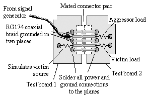
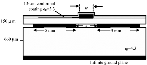
  • Connector crosstalk in open-pin-field connectors acts through a transformer-like principle.
  • Separating the loops of signal current within a connector by providing private power or ground pins for each signal reduces crosstalk.
  • Reducing the current in the aggressive circuit reduces crosstalk.


5.4.2 Through-Hole Clearances

Article first published in EDN Magazine , July 8, 1999

November 22, 5:45 a.m .

Ernie awoke with a start. It was still dark outside. His muscles tensed. Then, slowly, as his mind returned to consciousness, he began to relax. He always felt this way the morning after an all-night session in the lab ”especially a session in which he'd discovered something important. He always feared that he would forget everything before he had a chance to write it all down and that his insight, his brilliant flash of inspiration, would melt away with the sun's first rays. It didn't. The ugly truth was still with him. Nothing was left to do now but craft his final message. Ernie stumbled into the kitchen to put on some coffee. Grumbling, he logged onto the main email server and began....

November 22, 6:22 a.m .

SENDER: Ernie

TO: Messrs Ulrich (VP Eng), Dagbottom (VP Mktg), Blumpf (Pres)

RE: Daily status report ”Day 39

I have isolated our product failures to the layout of the daughterboard connector. Whenever the main data bus switches from mostly zeros to mostly ones, crosstalk within the connector activates the "write" strobe on the main system EEPROM circuits. This failure is repeatable. It explains the slow degradation of our system performance, especially the failures to reboot (due to corruption of the EEPROM configuration data).

Last night, I finally pinpointed the source of the problem. I used a pulse generator to transmit some test signals through the connector, simulating the same voltage and current conditions that would exist during an actual bus transition. Assuming that my measurements are correct, in actual use, the connector will induce an aggregate crosstalk of more than 2V on the EEPROM write line.

Never assume your board is built according to the layout specification.


This amount of crosstalk was not supposed to happen. It is the result of a monumental grounding error. As you know, the daughterboard connector includes many ground pins. During the layout phase, I inspected the layout artwork and film to ensure that these pins were properly connected to the ground plane beneath this connector (Figure 5.23, part A).

Figure 5.23. Ernie designed the ground plane with appropriate clearances and plenty of ground pathways between connector pins (A). The fabrication shop enlarged the ground plane's clearances, cutting off some of the ground pathways and creating massive amounts of crosstalk (B).

graphics/05fig23.gif

Unfortunately ”for reasons I do not totally comprehend ”the fabrication shop did not build our boards according to the layout specification. I can demonstrate the problem by cutting the board along the dotted lines cut 1 and cut 2 in Figure 5.23, part B. If our boards were any good, the ground would remain electrically connected through the multiple ground pathways between pins. It doesn't. The clearance holes are too big. We'll have to order new boards .

My recommendation is that we immediately order a rush quantity of new boards and race to salvage at least a portion of our Christmas-deadline shipments. I regret that it has taken so long to resolve this problem. Because I couldn't directly see the inner layers , I assumed that the fabrication shop had built the board the way we asked.

November 22, 7:21 p.m .

SENDER: Ulrich

TO: Ernie

Our board vendor says that his company has always adjusted the trace widths, pad sizes, and clearances to meet our trace-impedance and finished-yield targets. He suggests that in the future you ask to check the finished film that they actually use after panelizing, instead of the film from our layout department. Alternatively, you could ask to see some preliminary unlaminated panels, which show the finished etching on the inside. X-ray services are also available to help you see the inner layers.

I hope this information will be useful to you in your next job. Because we will now surely miss the Christmas deadline, our board of directors has voted to shut down your project. I hope you don't take this action personally . Our pcb vendor says that mistakes like this one happen all the time.

POINT TO REMEMBER

  • Never assume your fabrication shop will build the board the way you ask. Always check.


5.4.3 Measuring Connectors

Article first published in EDN Magazine , May 10, 2001

I would like to replace one connector type with a different, less expensive model. How do I prove the two connectors have the same electrical characteristics? Also, how will the power and ground-pin assignments within the connector affect its performance?

”John Lin

Three basic measurements will do the job. All three measurements use a mated pair of connectors hand-soldered to a solid ground plane on each side (Figure 5.24).

Figure 5.24. A simple test setup can characterize signal transmission, crosstalk, and EMI.

graphics/05fig24.gif

On either side of the connector, ground all the pins that you will use for power or ground connections. Leave the other pins unconnected but accessible to your test equipment.

Ground-shift voltages generated by connectors drive many common EMI failure mechanisms.


First, test signal fidelity using a standalone signal generator to transmit a digital signal through the connector. Use the voltage and risetime that will be present in the finished system. Load, or terminate, the signal on the far side of the connector as you would normally so that you get realistic currents through the connector as well as realistic voltages. See if the signal looks okay after it passes through. This test is the easiest for a connector to pass.

If your signal generator has a 50- W output, and the coaxial cable is also 50 W , the connector under test will react as if a 50- W source is driving it. If you want to simulate a source impedance other than 50- W , use an impedance-matching pad. The most common difficulty associated with this test is a failure to appreciate the importance of keeping the hand-soldered connections extremely short. A hand-soldered test jig works fine up to about 100 Mb/s. For connectors operating at 500 Mb/s and above, the connector should be mounted with realistic vias and clearances using a layer stack designed for your application.

The signal-fidelity test tells you whether the connector impedance matches your transmission-line impedance. If it's a good match, the signal will shoot through unscathed. If it's a poor match, the initial signal edge may come through degraded, and you may also see subsequent residual reflections, depending on how you terminate the line.

Next prepare some victim pins for a crosstalk measurement. Terminate both ends of each victim signal pin with impedances that approximate the actual impedances that your system uses. For example, if low impedance sources drive your signals, then ground the source side of each victim signal pin as if a low impedance source is holding it in a zero state.

Make several measurements, and plot crosstalk versus the distance between aggressor and victim. From this plot you can estimate the worst-case aggregate crosstalk that might affect any particular victim.

The third test measures one form of EMI. Using the crosstalk measurement setup, tie a 6-ft wire onto the solid ground plane on one side of the connector. Stretch the wire horizontally across your (preferably wooden!) lab bench. Next, tie another 6-ft wire onto the solid ground plane on the other side of the connector. Stretch this wire horizontally in the other direction. You've just made a dipole transmitter.

Using a calibrated antenna and a sensitive spectrum analyzer, have an EMI engineer plot the received signal power as a function of frequency while you blast simulated data through one signal pin. If you can't detect the spectrum of the emissions from your connector against the fabric of your local background noise, increase the size of your transmitted signal, and then de-rate the measured results accordingly . Alternatively, do the measurement in an anechoic chamber . This measurement evaluates the ground-transfer impedance of the connector. When you pump high-frequency signal currents through a connector, the currents return to their sources through the ground (or power) pins of the connector. The returning signal currents passing through the ground-transfer impedance of the connector create tiny voltage shifts between the ground on one side of the connector and the ground on the other, driving the dipole antenna. These same tiny ground shifts also drive many common EMI failure mechanisms, which is why this test is a good way to measure EMI-shielding effectiveness.

Changing the number of power and ground pins in your layout will affect all three measurements. For open pin-field connectors, EMI changes inversely in proportion to the number of power and ground pins. Aggregate crosstalk changes inversely with the square of the number of power and ground pins. Signal fidelity improves when the configuration of power and ground pins immediately surrounding each signal pathway matches the correct trace impedance.

POINT TO REMEMBER

  • Three primary measures of connector performance are signal fidelity, crosstalk, and EMI.


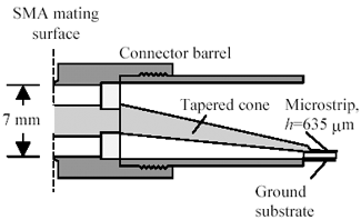
5.4.4 Tapered Transitions

Article first published in EDN Magazine , October 11, 2001

Consider the problem of adapting a straddle-mount SMA connector for a 10-Gbps digital application (Figure 5.25). The microwave guru who designed this particular SMA connector configured it to optimally launch into a gigantic microstrip measuring 1.52 mm (0.060 in.) wide suspended 0.81 mm (0.032 in.) above the nearest ground plane. Microwave circuits often incorporate such giant microstrips to curb skin-effect losses.

Figure 5.25. An SMA connector couples to a digital microstrip with an exponential CPW taper.

graphics/05fig25.gif

Your digital system probably uses much smaller microstrips with a much tighter trace-to-plane spacing. If you solder the straddle-mount SMA directly onto a small microstrip, it won't work properly. A small microstrip requires a ground plane much closer to the signal trace than does a large microstrip. With a tight signal-to-ground spacing, the parasitic capacitance between the SMA signal pin and your closely spaced ground plane will be too great, producing significant reflections. Assuming h = 150 m m (6 mils) for your digital microstrip, the excess parasitic capacitance of an SMA signal pad measuring 1.52 mm (0.060 in.) on a side is 0.69 pF, creating reflection coefficients at 1 and 5 GHz of 0.096 and 0.43 respectively. These reflection coefficients are unacceptably large. To make the circuit work at high speeds, you must reduce the parasitic capacitance of the SMA signal pin.

To reduce the parasitic capacitance, cut back the ground plane in the vicinity of the SMA signal pin. Figure 5.25 cuts back the ground plane in a beautifully tapered pattern reminiscent of a coplanar waveguide (CPW). It's not quite coplanar because the ground tracks on either side of the signal are offset down by one layer, but the effect is similar. For the purposes of this article, I'll call it a nearly-planar waveguide (NPW). The trace on layer 1 mimics the exponential taper of the cut in the ground plane. This tapered NPW converts the large geometry of the SMA footprint to the small geometry of a 250- m m (0.010-in.) microstrip trace while maintaining a constant 50- W impedance along its length. A tapered NPW defies analysis with 2-D quasistatic tools because its cross section changes along the length of the structure.

To reduce parasitic capacitance, cut back the ground plane in the vicinity of the SMA signal pin.


If your 2-D field solver computes ordinary CPW configurations, you can use it to design some appropriate trace and cut widths for various cross sections along the exponential taper, but don't expect those answers to be completely accurate. Your 2-D solver will improperly model the influence of the exponential taper on the impedance of the structure, and it may not understand that the signal and ground conductors are on different layers. Stretching the taper into a long, slowly evolving shape reduces the rate of change at any point, thus improving the accuracy of the 2-D solver. However, a long, gentle taper defeats your purpose ”you need a short taper. To obtain a short taper, you have to build a few topologies or simulate them with a 3-D solver and then adjust the design to correct its impedance.

A great example of a constant-impedance taper is the Eisenhart SMA connector (Figure 5.26 and [39] ). This connector uses a long, tapered metal cone inside the body of the connector to form a constant-impedance transition from the 7-mm connector body diameter to a microstrip measuring 1.2 mm (0.047 in.) wide. The Eisenhart connector uses a linear taper approximately 25 mm (1 in.) long. At frequencies as great as 18 GHz, the connector provides a reflection coefficient no worse than 7%.

Figure 5.26. An Eisenhart coaxial connector incorporates a conical taper.

(Figure adapted from K. C. Gupta et. al., Microstrip Lines and Slotlines , 2nd ed., Artech House, 1996 ISBN 0-89006-766-X)

graphics/05fig26.gif

The relative dimensions in the digital straddle-mount SMA layout are similar to those in the Eisenhart connector, so you should be able to use a similar rate of taper. Even better, the exponential transition, which etching technology enables, should provide even better performance than Eisenhart's linear taper. These factors indicate that a 1-in. exponential transition from the 1.52 mm SMA signal pad to a 250- m m trace should provide startlingly good performance from DC to 10 GHz. [39]

The values in Table 5.7 were generated using the coupled-line feature of Hyperlynx. They should provide a good starting place for your design of an NPW taper. Remember that these values won't be perfect, depending on the rate of taper adapted in your circuit. You'll have to build the structure (or simulate it with a 3-D field solver) and then tweak the geometry to get the TDR response just right.

Table 5.7. Fifty-Ohm NPW Configurations

Trace width w (mils)

Cut width s (mils)

Trace height h (mils)

10

6

14

4

6

15

8

6

17

12

6

24

24

6

32

36

6

39

48

6

48

64

6

58

96

6

60

128

6

The NPW table assumes the structure is made from a center trace of width w on layer 1, overlaid on top of a pair of big, fat ground traces on layer 2 (Figure 5.27). Each ground trace is 5 mm (0.200 in.) wide. The exact ground width on layer 2 doesn't much matter as long as it is at least 5 mm. The spacing between the ground traces on layer 2 (the ground-plane cut width) is s . The primary ground plane on layer 2 lies 150 m m (0.006 in.) beneath the surface.

Figure 5.27. Table 5.7 lists the impedance of an NPW configuration involving two ground traces (5 mm wide each, grounded at both ends) and one signal trace.

graphics/05fig27.gif

There is also a second ground plane in the circuit. The second plane is solid with no cut, lying 0.81 mm (0.032 in.) beneath the surface. The second ground helps reduce EMI from the taper structure and is required for my 2-D quasistatic field simulator to do its job.

All the ground features should be tied to each other and to the SMA ground lugs with copious quantities of vias.

The assumed dielectric constant of the board is 4.3. The traces are coated with a 13- m m (0.5-mil) conformal coating having a dielectric constant of 3.3.

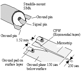
[39] The NPW technique usefully compensates for a signal-mounting pad that is too large given the signal-to-ground spacing of your board. The opposite problem (signal pad too small) is solved by adding capacitance to the signal pin (i.e., enlarging it).

POINT TO REMEMBER

  • A tapered transition maintains constant impedance when interconnecting transmission lines having widely different physical scales .


5.4.5 Straddle-Mount Connectors

High Speed Digital Design Online Newsletter , Vol 4, Issue 18

In response to my previous EDN column, (Section 5.4.4) "Tapered Transitions," I received numerous messages asking, What is a straddle-mount connector?

A straddle-mount connector is one designed to hang over the edge of a pcb, as opposed to a connector that sits up on one side of the board only.

Connectors that sit up on one side of the board are convenient for mechanical reasons, as they absorb almost no mechanical headroom below the plane of the board (beyond that required to clear the back sides of the through-hole pins, if they have them). The disadvantage of a one-sided connector is that the connector pins are necessarily displaced up above the plane of the board (and the plane of the circuits), meaning that your signals must travel up from the board, then across through the connector, and then back down on the other side. In doing so the signals will encounter some inevitable parasitic inductance and capacitance.

A straddle-mount connector locates all its pins close to the plane of the pcb. It is used only at the edge of a board, as some part of the mating assembly of the connector is usually designed to hang off the edge of the board, protruding down below the plane of the board. This style of connector requires mechanical headroom below the plane of the board.

It is called a straddle-mount connector because, when viewed from the side, the connector assembly appears to straddle the edge of the board, as opposed to " riding on top" of the board.

The main advantage of a straddle-mounted connector is the reduction in the distance your signal must flow when traversing the connector. Because no long pins are required to bring your signals up out of the plane of the board, the straddle-mount connector may achieve a much more intimate connection between the grounds of the two mated circuits than is otherwise possible using a connector that sits up on one side of the board only.

An example of a straddle-mounted (also called edge-mounted) SMA connector ”and I don't mean to imply it's the best one; it's just an example [40] ”is the Tyco Electronics P/N: 449692-1.

Another question I got was, What's an Eisenhart connector? The Eisenhart connector was a very old N-type connector documented in Gupta and Garg's book [39] . I mentioned it as an example of where someone successfully used the tapering principle. I didn't intend for anybody to rush out and buy one...and I can't find a supplier that has any. If you locate one that's still available, let me know. It may now go by a different name .

[40] At the time of publication, the Web link for this part was http://catalog.tycoelectronics.com/TE/docs/pdf/1/22/208221.pdf.

POINT TO REMEMBER

  • A straddle-mount connector locates all its pins close to the plane of the pcb.


5.4.6 Cable Shield Grounding

High Speed Digital Design Online Newsletter , Vol 2, Issue 2

I received numerous messages about cable grounding during my tenure as chief technical editor for the IEEE 802.3 Gigabit Ethernet standard. One part of that standard, the 1000BASE-CX link, runs at a data speed of 1.25 Gb/s (1.25 ·10 9 bits per second) over two-pair, 150-ohm, balanced cabling. The link uses one pair for the transmit direction and another pair for the receive direction. The 150-ohm balanced cabling has an overall shield.

Some of the correspondents questioned the need for grounding the cable shield to the equipment chassis at both ends, suggesting that it should be grounded at one end only. Others suggested capacitively coupling the cable shield to the chassis, or coupling through parallel R-C networks. These suggestions were made to allay concerns about large AC power currents that might flow through the shield, should the shield become connected to differing 60-Hz potentials at each end. Here's how I replied.

Reply

In high-speed digital applications, a low impedance connection between the shield and the equipment chassis at both ends is required in order for the shield to do its job. The shield connection impedance must be low in the frequency range over which you propose for the shield to operate . The measure of shield connection efficacy for a high-speed connector is called the ground-transfer impedance, or shield-transfer impedance, of the connector, and it is a crucial parameter.

In low-speed applications involving high-impedance circuitry , where most of the near-field energy surrounding the conductors is in the electric field mode (as opposed to the magnetic field mode), shields need only be grounded at one end. In this case the shield acts as a Faraday cage surrounding the conductors, preventing the egress (or ingress) of electric fields.

In high-speed applications involving low-impedance circuitry, most of the near-field energy surrounding the conductors is in the magnetic field mode, and for that problem, only a magnetic shield will work. That's what the double-grounded shield provides. Grounding both ends of the shield permits high-frequency currents to circulate through the shield, providing a magnetic shielding effect.

For a magnetic shield to operate properly, you must provide means for current to enter (or exit) at both ends of the cable. As a result, a low-impedance connection to the chassis, operative over the frequency range of our digital signals, is required at both ends of your shielded cable [49] .

How low an impedance is necessary? In the 1000BASE-CX cable the signal wires couple to the shield through an impedance of 75 ohms. That's another way of saying that the common-mode impedance of the cable is roughly 75 ohms. The standard requires that the shield be tied to the local chassis ground through an impedance of 0.1 ohm or less.

In such a configuration if you drive the signal wires with a common-mode voltage, you would expect to measure on the shield a voltage equal to (0.1/75) = 0.0013 times the common-mode voltage driven on the signal wires. The shield in this case should deliver a 57 dB shielding effectiveness. These are the specifications that our IEEE 802.3z 1000BASE-CX copper cabling group feels are necessary to meet FCC/VDE radiated emission regulations. In summary, the impedance between the shield and the chassis at the frequency of operation (about 1 GHz) must be less than 0.1 ohm.

To achieve such performance with a capacitively coupled shield, the effective series inductance of the capacitor would have to be limited to less than about 16 pico-henries. That small an inductance cannot be implemented in a leaded component ”you would need a very low-inductance distributed capacitance, possibly implemented as a thin gasket distributed all the way around the connector shell, insulating the connector shell from the chassis. We have seen proposals for this type of connector, but have not seen one work in actual practice.

The BERG MetaGig shielded connector exceeds the requirement for a shield transfer impedance. It does so by providing a direct metallic connection between chassis and shield that goes all the way around the connector pins, completely enclosing the signal conductors. A direct metallic connection is the only way we have found to beat the radiated emissions limits.

Keep in mind that the short copper link we are discussing (P802.3z clause 39) is intended for use inside a wiring closet. It only goes 25 meters . It will be used between pieces of equipment intentionally tied to the same ground (we call out in the specification that this must be the case). Between such pieces of equipment there will be no large circulating ground currents. For longer connections, we provide other links types that do not require grounding at either end ( multimode fiber, single mode fiber, and category-5 unshielded twisted pairs). Direct grounding of the shield at both ends is the correct choice for a short, high-speed connection.

POINT TO REMEMBER

  • A high-frequency shield needs direct metallic contact with the product chassis, completely surrounding the signal conductors.


Fundamentals

Transmission Line Parameters

Performance Regions

Frequency-Domain Modeling

Pcb (printed-circuit board) Traces

Differential Signaling

Generic Building-Cabling Standards

100-Ohm Balanced Twisted-Pair Cabling

150-Ohm STP-A Cabling

Coaxial Cabling

Fiber-Optic Cabling

Clock Distribution

Time-Domain Simulation Tools and Methods

Points to Remember

Appendix A. Building a Signal Integrity Department

Appendix B. Calculation of Loss Slope

Appendix C. Two-Port Analysis

Appendix D. Accuracy of Pi Model

Appendix E. erf( )

Notes


High-Speed Signal Propagation[c] Advanced Black Magic
ISBN: 013084408X
EAN: N/A
Year: 2005
Pages: 163

Flylib.com © 2008-2020.
If you may any questions please contact us: flylib@qtcs.net