Pcb Configurations
The requirements for high-speed differential traces in a solid-plane pcb are these:
- The two traces carry complementary voltages,
- The two traces carry complementary currents ”in conjunction with point 1 this implies that their characteristic impedances be the same,
- The two traces have equal impedances to the surrounding reference system ”ground planes, V CC planes, or both, and
- The two wires have equal propagation delay.
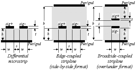
These requirements may be satisfied by many trace configurations. The most popular cases are the differential microstrip, the edge-coupled stripline , and the broadside- coupled stripline (Figure 6.12).
Figure 6.12. Differential pcb traces can be arranged in many different ways.
The author assumes you have access to a good 2-D field solver that can predict the differential impedance for various combinations of six variables : trace width, trace height, trace separation, trace thickness , configuration, and dielectric constant. If you don't have a 2-D field solver, then get one (it comes with any signal integrity package). Tell your manager I said you have to have it. A 2-D field solver is absolutely the best way to compute the impedance of any pcb transmission structure.
The following sections present some limited data on differential trace impedance, but don't expect to find all possible combinations of the six primary variables. I will concentrate instead on helping you understand the meaning and purpose of the various adjustments you can make to trace geometry.
6.10.1 Differential (Microstrip) Trace Impedance
 re . All AC parameters are specified at 1 GHz. The trace construction is assumed to be 1/2-oz etch plus 1/2-oz of plating , yielding a total 1-oz thickness, with a conformal coating (soldermask) consisting of a 12.7- m m (0.5-mil) layer having a dielectric constant of 3.3. If you select a different type of soldermask, your pcb vendor will adjust the trace width to compensate for the thickness of the dielectric material above the traces. A thicker soldermask will slightly reduce the finished propagation velocity.
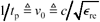 and c = 2.998 ·10 8 m/s.
6.10.2 Edge-Coupled Stripline
In a pcb application, the differential impedance of closely spaced traces varies with their spacing. As the gap between traces narrows, the differential impedance goes down. In extreme cases, the widths of the traces may require adjustment in order to keep the differential line impedance within a specified target range. This pesky adjustment in width is the one key disadvantage of closely spaced differential lines.
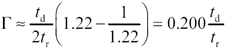
Figure 6.13 plots the impedance of edge-coupled differential traces versus spacing and trace width. The data for this plot were generated using a method-of-moments magnetic field simulator with 120 segments equally spaced around each pcb trace, with the current linearly interpolated across each segment.
Figure 6.13. Differential impedance Z DIFF (ohms) of edge-coupled differential striplines.
At small separations (less than 9 mils, as shown in Figure 6.13) the traces couple significantly, so the impedance varies with both trace width and spacing. When the intrapair separation exceeds about four times the trace height h (a separation of 24 mils in this example), the coupling between the two traces of the pair usually becomes so weak that the traces hardly affect each other. The differential impedance then depends mostly on just the trace width. At great separations the contours become completely vertical.
Very widely separated traces comprise an uncoupled or loosely coupled differential pair. For an uncoupled differential pair, the even-mode and odd-mode impedances are the same, and the differential impedance is twice the impedance of either line alone.
Differential traces can be pushed really, really close together. Squishing them together saves board area. If you do so, you will need to compute a new trace width to compensate for the fact that the differential impedance goes down for closely spaced pairs. Widely spaced pairs are not subject to this picky, difficult-to-implement requirement.
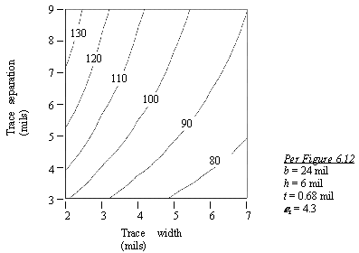
Another disadvantage of closely spaced pairs has to do with trace routing. Once the signals are closely paired, they cannot be separated, or else you will mess up their impedance (unless you readjust their widths). This effect imposes a routing penalty on edge-coupled traces, because it is difficult to get closely spaced, edge-coupled pairs to go around obstacles without temporarily separating them (Figure 6.14).
Figure 6.14. Closely spaced differential pairs can be difficult to route.
Finally, the use of tight coupling decreases the trace width, exacerbating the skin-effect loss.
What do I do? Unless absolutely pressed for space, I normally set the trace separation at about four times the trace height h . This setting usually yields a less-than -6% reduction in impedance, a small enough value to simply ignore. All stripline traces, differential or not, then have the same width. I instruct my layout professional to keep differential pairs near each other, but allow them to separate from time to time as needed to go around obstacles. I also insist that the elements of each pair be equal in length, to within 1/20 of a risetime, which limits the common-mode signal contributed by trace skew to less than 2.5% of the single-ended signal amplitude.
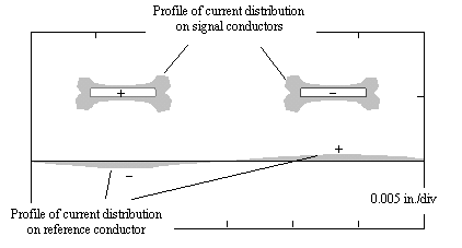
Figure 6.15 illustrates the magnetic lines of force surrounding an edge-coupled differential stripline pair. It shows intense concentrations of magnetic flux near the corners of the traces, indicating a substantial peaking of the current density at the corners. The proximity factor k p for these traces takes into account the crowding of current at the corners of the traces, plus a slight current concentration on the inside- facing surfaces of the pair, plus an allotment for the current induced on the top and bottom reference planes of the stripline cavity . The value of the proximity factor k p for the traces illustrated in Figure 6.15 is 3.08. Differential pcb traces with impedances between 100 to 150 ohms possess a proximity factor typically within the range of 2.5 to 3.5. Figure 6.16 illustrates the distribution of current around the periphery of the signal conductors, and also the lower reference plane. Current flows also on the upper reference plane, although that plane lies above the limits of the vertical scale in the drawing, so it is not shown.
Figure 6.15. This cross-sectional view of the magnetic field in the vicinity of a differential edge-coupled stripline shows intense field concentrations near the corners of the traces.
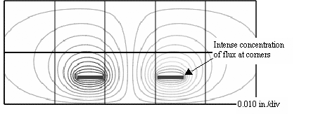
Figure 6.16. The distribution of current around the perimeter of a differential edge-coupled stripline takes on a dog-bone appearance, with the current peaking at the corners of the trace. The inside-facing corners of the pair have a slightly higher peak current than the outside-facing corners.
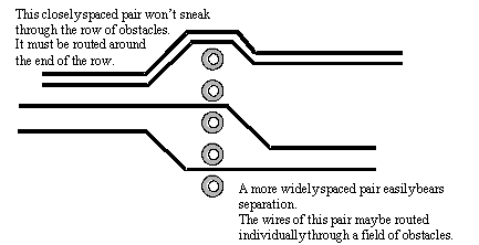
Figures 6.15 and 6.16 were generated using a 2-D field solver. This same program also calculates skin-effect resistance and skin-effect loss. A listing of such calculations for selected edge-coupled stripline geometries appears in Table 6.2. These values provide a good starting point for planning a high-speed interconnection. The table shows that the most important determiner of skin-effect loss is simply the trace width. All other factors are secondary.
If you don't find the configuration you need in the table, you may interpolate values of r SKIN and a R from the entries listed in the table. The interpolation process begins by first correcting the listed table values to account for your actual value of b . This is accomplished by scaling the trace geometry as follows :
- Select any row from the table with an interplane spacing b 2 that is reasonably close to your target b 1 .
- Compute the scaling constant k = b 1 / b 2 .
- Multiply h , w , s and also the trace thickness t by the constant k , producing a new row for the table.
- The impedance of the new row will be identical to the original Z DIFF .
- The skin-effect resistance (at 1 GHz) for the new row will equal the original r SKIN divided by k .
- The skin-effect attenuation constant for the new row will equal the original a r divided by k .
This scaling process is exact; however, it produces an unusual value of t (the thickness is usually standardized to either 1/2 or 1 oz of copper). Because t has only a second-order effect on characteristic impedance and resistance, you can usually ignore this change. Using the scaled values of b , h , w , and s while leaving t fixed will introduce some small inaccuracies into the scaling process, but still produce a new configuration with a characteristic impedance workably close to Z DIFF .
Once you have corrected a few of the table entries to account for your actual value of b , you can then interpolate along the h and w dimensions to estimate the skin-effect resistance and skin-effect loss.
This principle of scaling and interpolation works with the results from any field solver.
Example showing scaling of edge-coupled differential stripline
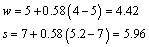
Suppose you have implemented a differential layout with b = 20, h = 7, w = 5, and s = 7. The skin-effect loss (Table 6.2) is 0.0929 dB/in versus a hypothetical budget of 0.1 dB/in.
How much can you squeeze the trace width without exceeding the skin-effect loss budget?
First let's try changing w and s without changing b . The next smallest trace size listed in Table 6.2 shows w = 4, s = 5.2, yielding a resistive loss of 0.1089 dB/in. You can adjust w and s 58% of the way towards this next smallest size, where the fraction 58% is determined by the ratio of skin-effect loss numbers :
Equation 6.16
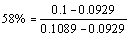
The interpolated values of w and s are
Equation 6.17
Next let's start the problem over, this time changing b . You have plenty of excess budget for skin effect loss in your initial configuration, so the new b can be smaller than the original, where the ratio of 93% is determined by the ratio of skin-effect losses:
Equation 6.18

Scaling all values by the factor 93% produces
Equation 6.19
This example has produced two new approximate configurations. The next step is to tweak the exact spacing s for each configuration to zero in on the exact impedance. This is done using your 2-D field solver. Then choose the exact interpair pitch to satisfy your crosstalk constraint. After that you will be in a position to determine which approach gives you the best layout density: just shrinking w and s while keeping b constant or shrinking b and everything else along with it.
POINTS TO REMEMBER
- Differential traces can be pushed really, really close together. If you do so, compute a new trace width to compensate for the fact that the differential impedance goes down for closely spaced pairs.
- Widely spaced (i.e., loosely-coupled) pairs are not subject to picky, difficult-to-implement spacing and width requirements.
- The most important determiner of skin-effect loss is the trace width.
- An interpair trace separation of four times h yields about a 6% effect on impedance, a small enough value in many cases to simply ignore.
- Matching the elements of each pair to within 1/20 of a risetime limits the common-mode signal contributed by trace skew to less than 2.5% of the single-ended signal amplitude.
Table 6.2. AC Resistance and Skin-Effect Loss (at 1 GHz) for Selected 100- W Differential Edge-Coupled Striplines
|
b |
h |
w |
s |
R AC W /in. |
R AC W /m |
a r dB/in. |
a r dB/m |
Z DIFF ( W ) |
|---|---|---|---|---|---|---|---|---|
|
10 |
3 |
3 |
40.0 |
3.50 |
137.8 |
0.152 |
5.99 |
99.0 |
|
10 |
4 |
3 |
7.0 |
3.24 |
127.6 |
0.139 |
5.47 |
100.4 |
|
10 |
5 |
3 |
7.0 |
3.22 |
126.8 |
0.137 |
5.40 |
101.2 |
|
10 |
5 |
4 |
40.0 |
2.76 |
108.7 |
0.126 |
4.95 |
94.6 |
|
14 |
4 |
3 |
5.5 |
3.19 |
125.6 |
0.136 |
5.36 |
101.0 |
|
14 |
4 |
4 |
12.0 |
2.74 |
107.9 |
0.118 |
4.63 |
100.3 |
|
14 |
5 |
3 |
4.5 |
3.14 |
123.6 |
0.135 |
5.31 |
100.1 |
|
14 |
5 |
4 |
7.5 |
2.60 |
102.4 |
0.112 |
4.39 |
100.5 |
|
14 |
5 |
5 |
40.0 |
2.33 |
91.7 |
0.101 |
3.98 |
99.5 |
|
14 |
7 |
3 |
4.5 |
3.11 |
122.4 |
0.132 |
5.19 |
101.8 |
|
14 |
7 |
4 |
6.5 |
2.56 |
100.8 |
0.110 |
4.31 |
100.6 |
|
14 |
7 |
5 |
13.0 |
2.24 |
88.2 |
0.096 |
3.77 |
100.9 |
|
14 |
7 |
6 |
40.0 |
2.01 |
79.1 |
0.091 |
3.59 |
95.0 |
|
20 |
5 |
3 |
4.4 |
3.14 |
123.6 |
0.134 |
5.28 |
101.0 |
|
20 |
5 |
4 |
6.5 |
2.59 |
102.0 |
0.111 |
4.37 |
100.7 |
|
20 |
5 |
5 |
11.0 |
2.27 |
89.4 |
0.097 |
3.84 |
100.6 |
|
20 |
5 |
6 |
40.0 |
2.09 |
82.3 |
0.092 |
3.61 |
98.4 |
|
20 |
7 |
3 |
3.9 |
3.13 |
123.2 |
0.134 |
5.26 |
101.1 |
|
20 |
7 |
4 |
5.2 |
2.55 |
100.4 |
0.109 |
4.29 |
100.9 |
|
20 |
7 |
5 |
7.0 |
2.17 |
85.4 |
0.093 |
3.66 |
100.7 |
|
20 |
7 |
6 |
10.0 |
1.91 |
75.2 |
0.082 |
3.24 |
100.3 |
|
20 |
7 |
7 |
19.0 |
1.75 |
68.9 |
0.075 |
2.96 |
100.7 |
|
20 |
7 |
8 |
40.0 |
1.61 |
63.4 |
0.072 |
2.85 |
96.3 |
|
20 |
10 |
3 |
3.7 |
3.14 |
123.6 |
0.135 |
5.30 |
100.6 |
|
20 |
10 |
4 |
5.0 |
2.54 |
100.0 |
0.108 |
4.25 |
101.6 |
|
20 |
10 |
5 |
6.5 |
2.15 |
84.6 |
0.092 |
3.60 |
101.4 |
|
20 |
10 |
6 |
8.5 |
1.88 |
74.0 |
0.081 |
3.17 |
100.7 |
|
20 |
10 |
7 |
12.0 |
1.68 |
66.1 |
0.072 |
2.85 |
100.5 |
|
20 |
10 |
8 |
25.0 |
1.56 |
61.4 |
0.067 |
2.65 |
100.3 |
|
30 |
5 |
3 |
4.3 |
3.15 |
124.0 |
0.135 |
5.30 |
100.7 |
|
30 |
5 |
4 |
6.3 |
2.60 |
102.4 |
0.111 |
4.38 |
100.7 |
|
30 |
5 |
5 |
10.0 |
2.27 |
89.4 |
0.097 |
3.83 |
100.7 |
|
30 |
5 |
6 |
22.0 |
2.09 |
82.3 |
0.090 |
3.54 |
100.2 |
|
30 |
6 |
3 |
4.0 |
3.14 |
123.6 |
0.134 |
5.27 |
101.0 |
|
30 |
6 |
4 |
5.4 |
2.56 |
100.8 |
0.110 |
4.33 |
100.7 |
|
30 |
6 |
5 |
7.5 |
2.20 |
86.6 |
0.094 |
3.71 |
100.7 |
|
30 |
6 |
6 |
11.2 |
1.96 |
77.2 |
0.084 |
3.31 |
100.6 |
|
30 |
6 |
7 |
20.0 |
1.81 |
71.3 |
0.078 |
3.07 |
100.4 |
|
30 |
7 |
3 |
3.8 |
3.14 |
123.6 |
0.134 |
5.29 |
100.9 |
|
30 |
7 |
4 |
5.0 |
2.56 |
100.8 |
0.109 |
4.31 |
100.9 |
|
30 |
7 |
4.5 |
5.7 |
2.35 |
92.5 |
0.101 |
3.96 |
100.7 |
|
30 |
7 |
5 |
6.5 |
2.17 |
85.4 |
0.093 |
3.67 |
100.6 |
|
30 |
7 |
6 |
8.8 |
1.91 |
75.2 |
0.082 |
3.22 |
100.7 |
|
30 |
7 |
7 |
12.5 |
1.73 |
68.1 |
0.074 |
2.92 |
100.8 |
|
30 |
7 |
8 |
21.0 |
1.60 |
63.0 |
0.069 |
2.72 |
100.5 |
|
30 |
8 |
3 |
3.7 |
3.15 |
124.0 |
0.134 |
5.29 |
101.0 |
|
30 |
8 |
4 |
4.7 |
2.56 |
100.8 |
0.110 |
4.33 |
100.6 |
|
30 |
8 |
5 |
6.0 |
2.17 |
85.4 |
0.093 |
3.66 |
100.7 |
|
30 |
8 |
6 |
7.7 |
1.89 |
74.4 |
0.081 |
3.20 |
100.6 |
|
30 |
8 |
7 |
10.2 |
1.69 |
66.5 |
0.073 |
2.85 |
100.9 |
|
30 |
8 |
8 |
14.0 |
1.55 |
61.0 |
0.066 |
2.62 |
100.6 |
|
30 |
8 |
9 |
23.0 |
1.45 |
57.1 |
0.062 |
2.45 |
100.5 |
|
30 |
8 |
10 |
40.0 |
1.36 |
53.5 |
0.060 |
2.37 |
97.8 |
|
30 |
10 |
3 |
3.6 |
3.16 |
124.4 |
0.135 |
5.30 |
101.2 |
|
30 |
10 |
4 |
4.5 |
2.57 |
101.2 |
0.110 |
4.32 |
101.0 |
|
30 |
10 |
5 |
5.5 |
2.17 |
85.4 |
0.093 |
3.67 |
100.7 |
|
30 |
10 |
6 |
6.8 |
1.89 |
74.4 |
0.081 |
3.19 |
100.7 |
|
30 |
10 |
7 |
8.4 |
1.67 |
65.7 |
0.072 |
2.82 |
100.9 |
|
30 |
10 |
8 |
10.5 |
1.51 |
59.4 |
0.065 |
2.55 |
100.8 |
|
30 |
10 |
9 |
13.5 |
1.38 |
54.3 |
0.059 |
2.34 |
100.6 |
|
30 |
10 |
10 |
19.0 |
1.29 |
50.8 |
0.055 |
2.18 |
100.6 |
|
30 |
10 |
11 |
34.0 |
1.22 |
48.0 |
0.053 |
2.08 |
100.2 |
|
30 |
10 |
12 |
40.0 |
1.15 |
45.3 |
0.052 |
2.03 |
96.4 |
|
30 |
15 |
3 |
3.5 |
3.17 |
124.8 |
0.135 |
5.33 |
101.0 |
|
30 |
15 |
4 |
4.3 |
2.58 |
101.6 |
0.111 |
4.36 |
100.7 |
|
30 |
15 |
5 |
5.3 |
2.18 |
85.8 |
0.093 |
3.65 |
101.2 |
|
30 |
15 |
6 |
6.3 |
1.89 |
74.4 |
0.081 |
3.19 |
100.9 |
|
30 |
15 |
7 |
7.5 |
1.67 |
65.7 |
0.072 |
2.82 |
101.0 |
|
30 |
15 |
8 |
9.0 |
1.50 |
59.1 |
0.064 |
2.53 |
100.9 |
|
30 |
15 |
9 |
11.0 |
1.36 |
53.5 |
0.058 |
2.30 |
101.0 |
|
30 |
15 |
10 |
13.0 |
1.25 |
49.2 |
0.054 |
2.14 |
100.0 |
|
30 |
15 |
11 |
17.0 |
1.17 |
46.1 |
0.050 |
1.98 |
100.3 |
|
30 |
15 |
12 |
25.0 |
1.10 |
43.3 |
0.047 |
1.87 |
100.5 |
|
NOTE (1) ”All values b , h , w , and s in mils. NOTE (2) ”AC parameters R AC , a r , and Z DIFF specified at 1 GHz with FR-4 dielectric NOTE (3) ”These stripline examples assume copper traces of 1/2-oz thickness with s = 5.98.10 7 S/m. |
||||||||
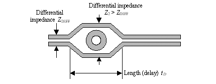
6.10.3 Breaking Up a Pair
Article first published in EDN Magazine , November 9, 2000The two traces comprising a differential pair, when routed close together, share a certain amount of cross-coupling. This coupling lowers the differential impedance between the traces. For example, when two traces with Z =50 W are well separated (uncoupled), the differential impedance between them should be precisely Z DIFF = 2 Z = 100 W . When you jam the same two traces close together (tightly coupled), as you might do to improve routing density, the differential impedance will be a lower value, perhaps something in the range of 70 to 90 W . Model the mismatched region as a short transmission line of impedance Z DIFF plus a lumped inductance L EXCESS . If the coupling effect lowers the differential impedance too much for your taste, you can fix it. Just reduce the trace widths, thus raising their impedance. The traces remain coupled, but you can (theoretically) always push the differential impedance back up to 100 W by making the traces skinnier. [49] What happens to a tightly coupled pair when it traverses an obstacle, such as a via (Figure 6.17)? If you have room to route both traces on the same side of the obstacle , maintaining their constant separation, no special problems arise. If, on the other hand, you separate the traces to pass by, then the differential impedance in the separated region reverts to its original, uncoupled value of 2 Z . If you have thinned the trace widths to produce exactly 100 W in the coupled state, then the reverted, uncoupled impedance with skinny traces will exceed 100 W . Figure 6.17. The impedance of a tightly-coupled differential pair changes when you separate the wires.
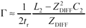
To calculate (approximately) the effects of such a mismatch, let's assume you have a long, uniform differential transmission configuration with differential impedance Z DIFF . Insert into the middle of this line a short section with differential impedance Z 2 , having length (in time) t d . Further assume that t d is much less than the signal risetime (or fall time) t r , so the mismatched section acts as a simple lumped-element circuit. Analysis begins by computing the values L 2 and C 2 corresponding to the mismatched section: The value L N is the natural inductance you would expect to accompany capacitance C 2 in a differential transmission line with differential impedance Z DIFF , as evidenced by the ratio Inductor L EXCESS represents the excess inductance in the mismatch region above and beyond L N . In other words, this procedure models the mismatch region as a short transmission line of impedance Z DIFF (comprising L N and C 2 ) plus a series inductance L EXCESS . You will next model the reflection generated by component L EXCESS . When a fast step input hits any small inductive discontinuity, you get a reflected pulse. The pulse duration equals the rise (or fall) time of the incoming step. You can approximate the reflection coefficient G (ratio of reflected pulse height to the incoming step size) generated by L EXCESS as follows: Equation 6.20
Substituting the definition of L EXCESS yields Equation 6.21
Further substituting your basic expressions for L 2 and C 2 gives Equation 6.22
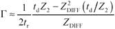
And consolidating the terms provides Equation 6.23
That's about the best approximation you will find for the case of a short separation between the elements of a differential pair. If you want better accuracy, use a time-domain simulator. In the example of Figure 6.17, supposing the ratio of Z 2 /Z DIFF to be (122 W )/(100 W )=1.22, equation [6.23] reduces to Equation 6.24
If this amount of signal degradation is troublesome , try thickening the traces in the separated region to match the impedance of the thinner, more highly coupled traces elsewhere. If you've kept t d / t r less than 1/6, you can expect a proportional accuracy of a couple of percentage points from approximation [6.23]. If you try to stretch the approximation to a ratio of t d / t r as big as 1/3, expect the approximation to be good only to about 20%. Beyond that, at t d / t r = 1/2 it falls completely apart, delivering totally erroneous answers. The same approximation works for BGA layouts, where signals escaping from the inner rows neck down to pass through the BGA ball field. The neck-down region raises the local trace impedance in a small region. In the event your separated traces pass particularly close to the edges of a via pad, the parasitic capacitance between your trace and the via may add to the value of C 2 in a noticeable way, modifying the values of L N , L EXCESS , and the reflection coefficient G . If the parasitic capacitance is large enough to produce a negative value of L EXCESS (meaning that the effective impedance Z 2 within the mismatched region is less than Z DIFF ), then your analysis must begin with the known value of L 2 and then compute the excess capacitance above and beyond that necessary to balance out the inductance L 2 . It so happens that the reflection coefficient for the case of Z 2 < Z DIFF is also given by equation [6.23]. The negative amplitude associated with the result in that case indicates that a positive-going step edge produces a negative reflected pulse. |
 and
and  . Next, mentally break into two pieces,
  , with
  .
. .
.
[49] You must avoid placing the traces so close together that the required trace width becomes unmanufacturable.
POINT TO REMEMBER
- If you separate elements of a tightly-coupled pair the differential impedance reverts to twice the uncoupled value of Z .
6.10.4 Broadside-Coupled Stripline
Figure 6.18 plots the impedance of broadside-coupled differential traces versus spacing and trace width. The data for this plot were generated using a method-of-moments magnetic field simulator with 120 segments equally spaced around each pcb trace, with the current linearly interpolated across each segment.
Figure 6.18. Differential impedance Z DIFF (ohms) of broadside-coupled differential striplines.
As you can see in the figure, widening the traces always decreases the differential impedance. Making the traces skinnier always raises the impedance.
Changing the height invokes a more complicated behavior. The impedance is maximized by a trace height (to the centerline of the trace) of 25% of the interplane separation (6 mils, as drawn in the figure).
From the 25% maximal point, a reduction in h moves the traces nearer to the planes, increasing the trace capacitance to the planes. This maneuver reduces the characteristic impedance. The more tightly you press the traces against the planes, the less direct coupling exists between the traces themselves .
Going in the other direction from the 25% maximal point, an increase in h moves the traces nearer to each other ( s gets smaller). This increases the direct capacitance between the two traces. This maneuver also reduces the characteristic impedance. The closer you bring the traces towards each other, the greater the coupling between traces.
At the 25% maximum-impedance-point the trace impedance is least sensitive to changes in width or height. Also, given a fixed interplane spacing, the 25%-point also maximizes the trace width, thus minimizing the skin-effect losses.
The only disadvantage to the 25%-point is that it maximizes crosstalk between adjacent broadside-coupled pairs; however, the advantages to be gained in trace pitch don't seem to this author to justify the penalties associated with using any trace height much different from 25%.
When converting from an edge-coupled pair on the surface layer of a pcb to a broadside-coupled pair on the inner layers , there is a subtle asymmetry built into the conversion. The asymmetry is illustrated in Figure 6.19.
Figure 6.19. The diversion through X in the path of returning signal current for signal A creates more delay than for trace B (cutaway view).
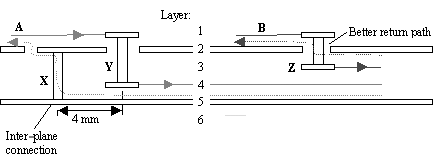
In the figure, signal A starts on layer 1 and then proceeds through blind via Y to layer 4. The signal current has no difficulty changing layers at this position; it just passes through Y . The return current associated with signal A ( dotted line) has a more difficult time managing the layer transition. At the left of the figure, the return current for A is shown flowing on the top surface of solid plane layer 2. In the center of the figure, most of the return current for this trace flows on solid plane layer 5 (returning signal current always flows mostly on the nearest solid plane). In the vicinity of the blind via, the return current must find some path (other than the capacitance of the planes, which is not terribly significant) through which it can hop from layer 2 to layer 5. Wherever a signal changes reference planes, the return current must always find a way to follow along.
In the figure, because planes 2 and 5 happen to carry the same potential, they are connected with via X , which forms the path for returning signal current. If the planes carry different voltages, the return-current path must traverse a bypass capacitor . In either case the returning signal current temporarily diverts away from the signal current.
The return current associated with signal B displays no such difficulty. At the position of blind via Z the returning signal current (dotted line) merely needs to change from the top surface of solid plane layer 2 to the bottom surface of that same layer. [50] As you can see, there is a clearance hole located at blind via position Z on layer 2. The returning signal current easily pops through this hole from one side of the plane to the other. There is no significant diversion of signal and return current at this location.
[50] The reference planes in a pcb are many skin depths thick; high-speed currents do not penetrate the planes, but rather flow only on one surface or the other of the plane.
The effect of the dissimilarity in return paths is that signal A experiences an extra delay as the return current finds its way from plane to plane. To minimize this additional delay, make sure you put a number of plane-to-plane connections near any points where the signals dive into an over/under configuration, where they change layers within the board, and again where they emerge.
Blind vias are used in Figure 6.19 for illustrative purposes; the same effect applies to through-hole vias.
Example showing asymmetry in broadside configuration
The broadside-coupled layout illustrated in Figure 6.19 includes two traces, A and B , that begin on the surface layer of the pcb and then pass through layer 2 into a broadside-coupled stripline configuration on layers 3 and 4. The plane-stitching via X is located 4 mm away from signal via Y . The return current for trace A therefore has to divert 4 mm out of its way to find the plane-stitching via, plus another 4 mm to get back, giving a total estimated additional delay of (4 mm) ·2 ·(4 ps/mm) = 56 ps. If this same asymmetry exists at both ends of the broadside configuration, the total additional delay on trace A equals 112 ps.
This crude estimate doesn't perfectly model what happens, as both the capacitance and the inductance of the via configuration are involved, but if an intrapair skew number anywhere near 100 ps matters to you, then either place the plane-stitching vias closer to the signal vias or don't use a broadside configuration.
In addition to possible asymmetry caused by imbalances in the return paths, the broadside configuration falls prey to any differences between the AC voltages on the two planes. Because the top trace is coupled more heavily to the top plane, and the bottom trace to the bottom plane, any differences in the voltages on these two planes induce a differential signal on the two traces. When using the broadside configuration, it pays to use the same power-supply voltage on both planes and nail them together with numerous vias on a tight grid. I like to use whatever plane voltage delivers the best common-mode noise rejection at the receiver (usually the ground plane).
If you use different power-supply voltages on the two planes, all the power-supply noise between them couples directly into the differential broadside-coupled configuration. In the side-by-side configuration, both traces naturally couple equally to the same nearby plane, so differential pickup of power-supply noise doesn't happen.
Broadside-coupled traces suffer from the dielectric layer-thickness tolerances on the layers separating the traces from their respective solid planes. For example, in a design with 5-mil separation from each trace to its respective plane, a layer-thickness tolerance of +/ “ 1 mil might result in one trace being 4 mils and the other 6 mils away from the reference planes. This arrangement impairs your ability to achieve good symmetry between the traces, which is after all the whole purpose of using a differential configuration. Edge-coupled traces, because they are etched at the same time under the same conditions on the same layer with the same layer thickness, are generally more symmetric.
The impedance of a broadside-coupled trace is affected by the mechanical registration tolerance of the two signal layers (3 and 4 in Figure 6.19).
The one possible area where broadside-coupled traces have an advantage over edge-coupled traces is routing density. For example, if you need to interleave a large bus through a succession of connector pin fields on a large backplane, the broadside configuration requires only single-track routing between pins, whereas an edge-coupled configuration might require double-track routing between pins to achieve the same layout density. The broadside configuration is also somewhat easier to lay out by hand, because both traces go everywhere together (except at the launch and recovery sites). I avoid broadside-coupled traces unless they are made necessary by routing considerations.
Figure 6.20 illustrates the magnetic lines of force surrounding a broadside-coupled differential pair. It shows intense concentrations of magnetic flux near the corners of the traces, indicating a substantial peaking of the current density at the corners. The proximity factor k p for these traces takes into account the crowding of current at the corners of the traces, plus any current concentrations on flat surfaces of the pair, plus an allotment for the current induced on the top and bottom reference planes of the stripline cavity. The proximity factor for the traces illustrated in Figure 6.20 is 2.73. [51] Differential broadside-coupled pcb traces with impedances between 75 to 135 ohms possess a proximity factor typically within the range of 2.5 to 3.5.
[51] The proximity factor is the ratio of the actual AC resistance to the resistance one would compute assuming current distributed uniformly around the periphery of one signal conductor only, and taking into account the skin depth.
Figure 6.20. This cross-sectional view of the magnetic field in the vicinity of a broadside-coupled stripline shows intense field concentrations near the corners of the traces.
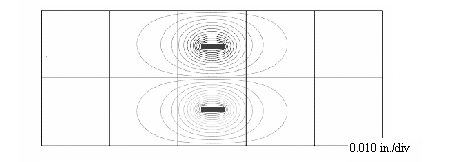
Table 6.3 presents the skin-effect resistance and skin-effect attenuation for selected broadside-coupled stripline configurations.
If you need results for some value b 1 that does not appear in the table, you can linearly interpolate the values in the table to accommodate an intermediate value of b , using the b -column as the x -axis and any other column as the y -axis in your interpolation.
POINTS TO REMEMBER
- Broadside differential trace impedance is maximized by a trace height equal to 25% of the interplane separation.
- The bottom trace of a broadside-coupled differential pair has some extra delay built in at the endpoints.
- Avoid broadside-coupled traces unless they are made necessary by routing considerations.
Table 6.3. AC Resistance and Skin-Effect Loss (at 1 GHz) for Selected 100- W Differential Broadside-Coupled Striplines
|
b mil |
h mil |
w mil |
R AC W /in.@1GHz |
R AC W /m@1GHz |
a r dB/in.@1GHz |
a r dB/m@1GHz |
|---|---|---|---|---|---|---|
|
14 |
4 |
1.9 |
4.04 |
159.1 |
0.175 |
6.89 |
|
20 |
5 |
3.5 |
2.71 |
106.5 |
0.117 |
4.61 |
|
30 |
7 |
5.3 |
2.01 |
78.9 |
0.087 |
3.43 |
|
45 |
10 |
9.1 |
1.32 |
52.0 |
0.057 |
2.24 |
|
NOTE(1) ”All values b , h , and w in mils. NOTE(2) ”AC parameters R AC , and a r specified at 1 GHz with FR-4 dielectric NOTE(3) ”These stripline examples assume copper traces of 1/2-oz thickness with s = 5.98 ·10 7 S/m. |
||||||
Fundamentals
- Impedance of Linear, Time-Invariant, Lumped-Element Circuits
- Power Ratios
- Rules of Scaling
- The Concept of Resonance
- Extra for Experts: Maximal Linear System Response to a Digital Input
Transmission Line Parameters
- Transmission Line Parameters
- Telegraphers Equations
- Derivation of Telegraphers Equations
- Ideal Transmission Line
- DC Resistance
- DC Conductance
- Skin Effect
- Skin-Effect Inductance
- Modeling Internal Impedance
- Concentric-Ring Skin-Effect Model
- Proximity Effect
- Surface Roughness
- Dielectric Effects
- Impedance in Series with the Return Path
- Slow-Wave Mode On-Chip
Performance Regions
- Performance Regions
- Signal Propagation Model
- Hierarchy of Regions
- Necessary Mathematics: Input Impedance and Transfer Function
- Lumped-Element Region
- RC Region
- LC Region (Constant-Loss Region)
- Skin-Effect Region
- Dielectric Loss Region
- Waveguide Dispersion Region
- Summary of Breakpoints Between Regions
- Equivalence Principle for Transmission Media
- Scaling Copper Transmission Media
- Scaling Multimode Fiber-Optic Cables
- Linear Equalization: Long Backplane Trace Example
- Adaptive Equalization: Accelerant Networks Transceiver
Frequency-Domain Modeling
- Frequency-Domain Modeling
- Going Nonlinear
- Approximations to the Fourier Transform
- Discrete Time Mapping
- Other Limitations of the FFT
- Normalizing the Output of an FFT Routine
- Useful Fourier Transform-Pairs
- Effect of Inadequate Sampling Rate
- Implementation of Frequency-Domain Simulation
- Embellishments
- Checking the Output of Your FFT Routine
Pcb (printed-circuit board) Traces
- Pcb (printed-circuit board) Traces
- Pcb Signal Propagation
- Limits to Attainable Distance
- Pcb Noise and Interference
- Pcb Connectors
- Modeling Vias
- The Future of On-Chip Interconnections
Differential Signaling
- Differential Signaling
- Single-Ended Circuits
- Two-Wire Circuits
- Differential Signaling
- Differential and Common-Mode Voltages and Currents
- Differential and Common-Mode Velocity
- Common-Mode Balance
- Common-Mode Range
- Differential to Common-Mode Conversion
- Differential Impedance
- Pcb Configurations
- Pcb Applications
- Intercabinet Applications
- LVDS Signaling
Generic Building-Cabling Standards
- Generic Building-Cabling Standards
- Generic Cabling Architecture
- SNR Budgeting
- Glossary of Cabling Terms
- Preferred Cable Combinations
- FAQ: Building-Cabling Practices
- Crossover Wiring
- Plenum-Rated Cables
- Laying Cables in an Uncooled Attic Space
- FAQ: Older Cable Types
100-Ohm Balanced Twisted-Pair Cabling
- 100-Ohm Balanced Twisted-Pair Cabling
- UTP Signal Propagation
- UTP Transmission Example: 10BASE-T
- UTP Noise and Interference
- UTP Connectors
- Issues with Screening
- Category-3 UTP at Elevated Temperature
150-Ohm STP-A Cabling
- 150-Ohm STP-A Cabling
- 150- W STP-A Signal Propagation
- 150- W STP-A Noise and Interference
- 150- W STP-A: Skew
- 150- W STP-A: Radiation and Safety
- 150- W STP-A: Comparison with UTP
- 150- W STP-A Connectors
Coaxial Cabling
- Coaxial Cabling
- Coaxial Signal Propagation
- Coaxial Cable Noise and Interference
- Coaxial Cable Connectors
Fiber-Optic Cabling
- Fiber-Optic Cabling
- Making Glass Fiber
- Finished Core Specifications
- Cabling the Fiber
- Wavelengths of Operation
- Multimode Glass Fiber-Optic Cabling
- Single-Mode Fiber-Optic Cabling
Clock Distribution
- Clock Distribution
- Extra Fries, Please
- Arithmetic of Clock Skew
- Clock Repeaters
- Stripline vs. Microstrip Delay
- Importance of Terminating Clock Lines
- Effect of Clock Receiver Thresholds
- Effect of Split Termination
- Intentional Delay Adjustments
- Driving Multiple Loads with Source Termination
- Daisy-Chain Clock Distribution
- The Jitters
- Power Supply Filtering for Clock Sources, Repeaters, and PLL Circuits
- Intentional Clock Modulation
- Reduced-Voltage Signaling
- Controlling Crosstalk on Clock Lines
- Reducing Emissions
Time-Domain Simulation Tools and Methods
- Ringing in a New Era
- Signal Integrity Simulation Process
- The Underlying Simulation Engine
- IBIS (I/O Buffer Information Specification)
- IBIS: History and Future Direction
- IBIS: Issues with Interpolation
- IBIS: Issues with SSO Noise
- Nature of EMC Work
- Power and Ground Resonance
Points to Remember
Appendix A. Building a Signal Integrity Department
Appendix B. Calculation of Loss Slope
Appendix C. Two-Port Analysis
- Appendix C. Two-Port Analysis
- Simple Cases Involving Transmission Lines
- Fully Configured Transmission Line
- Complicated Configurations
Appendix D. Accuracy of Pi Model
Appendix E. erf( )
Notes
EAN: N/A
Pages: 163
- Chapter V Consumer Complaint Behavior in the Online Environment
- Chapter VII Objective and Perceived Complexity and Their Impacts on Internet Communication
- Chapter IX Extrinsic Plus Intrinsic Human Factors Influencing the Web Usage
- Chapter XV Customer Trust in Online Commerce
- Chapter XVIII Web Systems Design, Litigation, and Online Consumer Behavior
