Pcb Signal Propagation
5.1.1 Characteristic Impedance and Delay
At this point in time, all major pcb CAD packages incorporate 2-D field solvers. These tools are extremely effective at calculating transmission-line impedance and delay, so much so that a listing of the old transmission-line impedance approximations would be of little use to the average reader. The values computed for impedance and delay correspond to the variables Z and v in the signal propagation model of Chapter 3.
If you don't already have a 2-D field solver, get one. If you absolutely cannot afford an automated tool, at least get a copy of Wadell [41] . His book lists all the closed-form approximation formulas for impedance and propagation delay of transmission-line configurations that were known as of the time of publication, including microstrips, striplines, some coplanar structures, and various differential arrangements. Failing that, this author modestly recommends the formula sets included in the appendices of [51] .
In a practical sense, what you need to know about pcb-trace impedance is that it varies approximately with the square root of trace height, inversely with the square root of width, and inversely with the square root of the effective dielectric constant. These variations are not exact, but indicate generally the sensitivity of trace impedance to the parameters of width and height. The trace thickness is a secondary parameter.
For striplines, the effective dielectric constant (and thus the delay) is entirely determined by the dielectric constant of the surrounding substrate material. For microstrips, the effective dielectric is somewhat less (see 5.1.3.1, "Estimating the Effective Dielectric Constant for a Microstrip"). Examples are given in Table 5.1.
Because parameters for skin-effect resistance and dielectric loss are less broadly disseminated, I shall endeavor to provide some guidance on those matters.
POINT TO REMEMBER
- If you don't already have a 2-D field solver, get one.
5.1.2 Resistive Effects
5.1.2.1 DC Resistance of Pcb Trace
The formula for the nominal DC resistance of a rectangular pcb trace is given in [2.41] (Section 2.4, "DC Resistance").
POINT TO REMEMBER
- A 1/2-oz copper pcb trace with 100- m m (3.9 mil) width has a DC resistance of 9.6 W /m. The DC resistance scales inversely with the width and inversely with the copper plating weight.
5.1.2.2 AC Resistance of Pcb Trace
The proximity effect for pcb traces takes hold at rather low frequencies on the order of a few megahertz . Below that frequency the magnetic forces due to changing currents in the traces are too small to influence the patterns of current flow. Low-frequency current in a pcb trace therefore follows the path of least resistance , filling the cross-sectional area of the trace, flowing uniformly throughout the signal conductor. That same current, as it returns to its source through the power-and-ground planes, tends to spread out in a wide, flat sheet, occupying as much of the surface area of the planes as possible on its way back to the source. That is the least resistive path through the planes.
Above w LC (a few Megahertz for most pcb traces) the magnetic forces surrounding a trace become quite significant, so much so that they change the patterns of current flow. The current is forced into a new distribution dependent not on the trace resistance, but on the trace inductance. This new distribution follows the path of least inductance , which is by definition that distribution of current that minimizes the total stored magnetic field energy surrounding the trace. Since the path of least inductance differs by definition from the path of least resistance, you would expect effective trace resistance to be increased when current is forced to flow in this high-frequency mode.
The magnetic fields constrain the high-frequency current in two ways. First, the current is confined to a shallow band of depth d around the perimeter of a conductor, increasing the apparent resistance of the trace. This increase in apparent resistance is called the skin effect.
Next , the magnetic fields distribute the current around the perimeter of the conductor in a non-uniform manner (the proximity effect). The relative increase in the apparent resistance of the conductor due to this non- uniformity , above and beyond what you would expect from the action of the skin effect alone, is represented by the proximity factor k p .
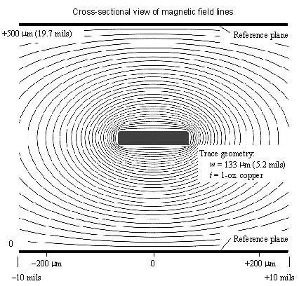
The proximity effect draws signal current towards the side of a microstrip facing the reference plane, or that side of a stripline that faces the nearest reference plane. It simultaneously concentrates the returning signal current on the reference plane, forming it into a narrow band that flows on the plane, staying mostly underneath the signal trace.
The increase in resistance of a typical high-speed digital signal conductor due to the proximity effect (above and beyond simple consideration of the skin depth and trace circumference assuming a uniform current distribution) typically ranges from 25% to 50%. This fraction remains fixed at all frequencies high enough for the effect to have taken hold (typically somewhere in the vicinity of w LC ).
Another similar- sized increase in resistive dissipation occurs due to the nonuniform distribution of current on the reference plane. At DC, you can assume that current spreads widely in all directions, so the DC reference-plane resistance should be (nearly) zero. At high frequencies, however, the returning signal current in the planes flows most heavily just underneath your trace, with wide tails of residual current falling off (at least) quadratically as you move away from the trace on either side. The current in this reference-plane distribution, because it remains well concentrated in a narrow band underneath the signal conductor, dissipates a noticeable amount of power, typically on the order of 25% to 50% of the signal-trace dissipation. This fraction remains fixed at all frequencies high enough for the effect to have taken hold.
The proximity factor takes into account the additional resistance due to redistribution of current on both the signal conductor and the reference planes.
Table 5.1 lists values of the AC resistance R and proximity factor k p for typical trace geometries used in high-speed digital designs. The value of R already incorporates k p ; I'm just showing the k p in case you want to use it to work out other similar configurations later and so you can see how gradually it changes with trace geometry.
In Table 5.1, parameter w is the trace width, h the height of the bottom surface of the trace above the lower reference plane, and b (striplines only) the separation between the planes (Figure 5.2). The microstrips listed in Table 5.1 assume 1-oz copper (including plating) with a conformal coating (soldermask) consisting of a 12.7- m m (0.5-mil) layer having a dielectric constant of 3.3. The stripline examples assume 1/2-oz bare copper. The resistance data was developed using a method-of-moments magnetic field simulator with 120 segments equally spaced around each pcb trace, with the current linearly interpolated across each segment, and three points at each corner rounded to fit a circular arc. The author estimates the accuracy of the data generated by this simulator at approximately +/ 2%.
Figure 5.2. Printed-circuit trace configurations are defined by parameters w , t , h , and b .
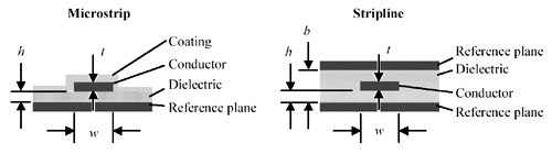
Table 5.1 assumes a dielectric constant of 4.3. If you are working with a different dielectric constant, you should know that what matters most for determining the proximity factor is the ratio w / h . The ratio t / h , assuming the trace is thin compared to its width, is of secondary importance. Traces with similar ratios of w / h inherit similar values of k p regardless of the dielectric constant.
Table 5.1 does not take into account either surface roughness or the inevitable random variations in trace width that occur in real boards .
Table 5.1. AC Resistance and Skin Effect Loss at 1 GHz for Selected Single-Ended Microstrips and Striplines
|
h mil |
w mil |
b mil |
R AC W /in. |
R AC W /m |
k p |
a r dB/in. |
a r dB/m |
Z W |
|
|---|---|---|---|---|---|---|---|---|---|
|
50-ohm microstrips, 1-oz copper with soldermask |
|||||||||
|
10 |
17.9 |
n/a |
0.420 |
16.5 |
1.953 |
.036 |
1.44 |
50 |
3.24 |
|
9 |
16.0 |
n/a |
0.460 |
18.1 |
1.928 |
.040 |
1.57 |
50 |
3.24 |
|
8 |
14.0 |
n/a |
0.513 |
20.2 |
1.903 |
.045 |
1.75 |
50 |
3.24 |
|
7 |
12.1 |
n/a |
0.578 |
22.7 |
1.878 |
.050 |
1.98 |
50 |
3.24 |
|
6 |
10.2 |
n/a |
0.663 |
26.1 |
1.851 |
.058 |
2.27 |
50 |
3.25 |
|
5 |
8.3 |
n/a |
0.780 |
30.7 |
1.820 |
.068 |
2.67 |
50 |
3.25 |
|
60-ohm microstrips, 1-oz copper with soldermask |
|||||||||
|
10 |
12.5 |
n/a |
0.531 |
20.9 |
1.776 |
.038 |
1.51 |
60 |
3.16 |
|
9 |
11.1 |
n/a |
0.583 |
23.0 |
1.754 |
.042 |
1.66 |
60 |
3.16 |
|
8 |
9.7 |
n/a |
0.648 |
25.5 |
1.731 |
.047 |
1.85 |
60 |
3.16 |
|
7 |
8.3 |
n/a |
0.730 |
28.8 |
1.704 |
.053 |
2.08 |
60 |
3.16 |
|
6 |
6.9 |
n/a |
0.839 |
33.0 |
1.675 |
.061 |
2.39 |
60 |
3.16 |
|
5 |
5.6 |
n/a |
0.981 |
38.6 |
1.650 |
.071 |
2.80 |
60 |
3.16 |
|
70-ohm microstrips, 1-oz copper with soldermask |
|||||||||
|
10 |
8.8 |
n/a |
0.665 |
26.2 |
1.631 |
.041 |
1.62 |
70 |
3.10 |
|
9 |
7.8 |
n/a |
0.728 |
28.7 |
1.609 |
.045 |
1.78 |
70 |
3.10 |
|
8 |
6.7 |
n/a |
0.813 |
32.0 |
1.584 |
.050 |
1.99 |
70 |
3.10 |
|
7 |
5.8 |
n/a |
0.905 |
35.6 |
1.566 |
.056 |
2.21 |
70 |
3.10 |
|
6 |
4.8 |
n/a |
1.036 |
40.8 |
1.542 |
.064 |
2.53 |
70 |
3.10 |
|
5 |
3.8 |
n/a |
1.215 |
47.8 |
1.516 |
.075 |
2.97 |
70 |
3.10 |
|
50-ohm striplines, 1/2-oz bare copper |
|||||||||
|
5 |
3.5 |
10 |
1.498 |
59.0 |
1.513 |
.013 |
5.12 |
50 |
4.30 |
|
5 |
5.1 |
15 |
1.144 |
45.0 |
1.597 |
.099 |
3.91 |
50 |
4.30 |
|
7 |
5.8 |
15 |
1.014 |
39.9 |
1.586 |
.088 |
3.47 |
50 |
4.30 |
|
5 |
5.7 |
20 |
1.074 |
42.3 |
1.655 |
.093 |
3.67 |
50 |
4.30 |
|
7 |
7.2 |
20 |
0.865 |
34.0 |
1.646 |
.075 |
2.96 |
50 |
4.30 |
|
10 |
8.0 |
20 |
0.782 |
30.8 |
1.637 |
.068 |
2.67 |
50 |
4.30 |
|
5 |
6.2 |
30 |
1.033 |
40.7 |
1.714 |
.090 |
3.53 |
50 |
4.30 |
|
7 |
8.5 |
30 |
0.782 |
30.8 |
1.732 |
.068 |
2.67 |
50 |
4.30 |
|
10 |
11.1 |
30 |
0.609 |
24.0 |
1.729 |
.053 |
2.08 |
50 |
4.30 |
|
15 |
12.7 |
30 |
0.533 |
21.0 |
1.722 |
.046 |
1.82 |
50 |
4.30 |
|
NOTESAC parameters R AC , a r , Z , |
|||||||||
The other columns listed in Table 5.1 are
- a r resistive trace loss (dB/m 1 GHz)
- Z real part of characteristic impedance ( W at 1 GHz)
 re dielectric constant (real part of effective relative electric permittivity) at 1 GHz
The propagation velocity v (m/s) and delay t p (s/m) are found from re , where  and c = 2.99810 8 m/s. The DC resistance constant k a is unity for all the single-ended pcb trace examples in Table 5.1.
Modern 2-D electromagnetic field solvers automatically calculate the proximity effect when reporting skin-effect resistance.
POINTS TO REMEMBER
- Low-frequency current in a pcb trace therefore follows the path of least resistance , filling the cross-sectional area of the trace.
- The skin effect confines high-frequency current to a shallow band of depth d around the perimeter of a conductor.
- The proximity effect draws signal current towards the side of a microstrip facing the reference plane, or that side of a stripline that faces the nearest reference plane.
- The increase in resistance of a typical high-speed digital signal conductor due to the proximity effect (above and beyond simple consideration of the skin depth and trace circumference assuming a uniform current distribution) typically ranges from 25% to 50%.
- Another similar-sized increase in resistive dissipation occurs due to the nonuniform distribution of current on the reference plane.
- Traces with similar ratios of w / h inherit similar values of k p regardless of the dielectric constant.
5.1.2.3 Calculation of Perimeter of Pcb Trace
When using [2.43], [2.44], or [2.63] to estimate the total series resistance R AC of the conductor, taking into account both skin effect and proximity effect, the perimeter of the signal conductor is defined
Equation 5.1

|
where |
p is the perimeter of the conductor (m), and |
|
w and t are the width and thickness of the signal conductor respectively (m). |
5.1.2.4 Very Low Impedance Pcb Trace
In the limit as the trace height h approaches zero (and the impedance descends towards zero), the trace concentrates all its current on the reference-plane facing side of the trace, with none on the reverse side. This doubling of the current density on one side doubles the apparent resistance. In addition, the trace suffers from an identical distribution of current on the reference plane, doubling the result again, for a total of k p  4.0.
4.0.
5.1.2.5 Calculation of Skin-Effect Loss Coefficient for Pcb Trace
The skin-effect loss in units of nepers per meter is given by [3.114]:
Equation 5.2
|
where |
R is the skin-effect resistance ( W /m) at the particular frequency w . |
|
NOTE: |
This formula applies only at frequencies above the onset of the skin effect. |
If the line resistance R ( w ) is specified as a function of frequency, the resistive loss coefficient in units of nepers per meter equals,
Equation 5.3
For microstrips, Pucel et al. [45] (and [52] , which is reproduced in [41] ) provide empirical closed-form approximations for the calculation of a r . A spot-check comparison of values from Pucel's closed-form expressions with the values listed for resistive loss in Table 5.1 reveals a corroboration error of about 2%.
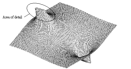
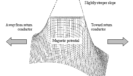
5.1.2.6 Popsicle-Stick Analysis
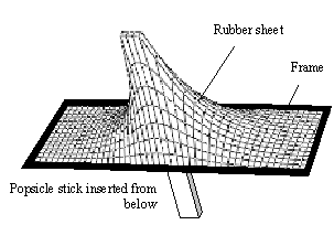
POINT TO REMEMBER
- You can simulate the magnetic field surrounding a pc-board stripline using a rubber sheet and a Popsicle stick.
5.1.2.7 Nickel-Plated Traces
POINT TO REMEMBER
- At frequencies on the order of 1 GHz, nickel-plating the top surface of a microstrip cuts in third the effective useful length of the trace.
5.1.3 Dielectric Effects
Microwave designers worry a lot about dielectric loss. The dielectric-loss problem is particularly acute when constructing high-Q circuits intended to ring without signal amplitude loss for many cycles. As a result, microwave designers often choose ceramic substrates, like alumina, that have excellent dielectric loss properties in the gigahertz regime . Digital designers typically avoid high-Q circuit topologies and so are not nearly as sensitive to dielectric loss.
For FR-4 digital circuit board applications at operating frequencies below 1 GHz (corresponding to the highest frequency of interest in the rising and falling edge spectra of a system with rise and fall times of 500 ps), at distances up to 10 inches, you may safely ignore dielectric losses. At longer distances or at higher speeds, dielectric losses can become quite significant.
POINTS TO REMEMBER
- For FR-4 digital circuit board applications with risetimes of 500 ps or slower, at distances up to 10 inches, you may ignore dielectric losses.
- At longer distances or at higher speeds, dielectric losses can become quite significant.
5.1.3.1 Estimating the Effective Dielectric Constant for a Microstrip
A stripline trace contains all (or most of) its electric fields within the dielectric cavity formed between two solid conducting reference planes. The dielectric properties of stripline traces therefore depend only on the dielectric constant and loss tangent of the pcb material.
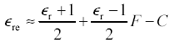
Microstrips, on the other hand, contain only part of their electric field within the dielectric layer. The remainder spews up into the air. The microstrip configuration therefore constitutes a type of mixture dielectric with properties intermediate between the properties of the dielectric substrate and air. The effective permittivity for a microstrip depends on the geometry of the trace and the proportion of total field energy stored in each of the two regions .
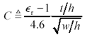
Many empirical closed-form approximations exist for the calculation of effective permittivity. The book by Gupta [39] provides numerous references for such approximations. The particular form of Gupta's equations reported here comes from a paper by I. J. Bahl and R. Garg [50] .
Equation 5.4
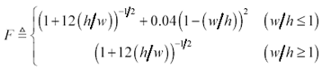
Equation 5.5
Equation 5.6
|
where |
w , h , and t are the width, height, and thickness respectively of a pcb microstrip (m), |
|
|
|
|
|
|
|
C and F are empirically derived constants, and |
|
|
no limits to accuracy or applicability were supplied with this equation. |
A spot-check comparison of values from Bahl and Garg's closed-form expression with the values for effective dielectric constant listed in Table 5.1 reveals a corroboration error of about 3%.
For striplines, re = r .
POINT TO REMEMBER
- A microstrip has dielectric properties intermediate between the properties of the dielectric substrate and air.
5.1.3.2 Propagation Velocity
From the effective dielectric constant re , you may determine the propagation velocity.
Equation 5.7

|
where |
c is the velocity of light in vacuum , 2.99810 8 m/s, |
|
|
|
|
v is the velocity of propagation (m/s). |
Examples showing the variation in re (and thus trace delay) for various microstrip trace geometries appear in Sections 5.1.3.6, "Passivation and Soldermask," 12.4, "Stripline vs. Microstrip Delay," and 6.10.1, "Differential (Microstrip) Trace Impedance." The effective relative permittivity for a stripline always equals the relative permittivity of the substrate material.
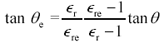
5.1.3.3 Calculating the Effective Loss Tangent for a Microstrip
For striplines, the loss tangent of the transmission configuration equals the loss tangent of the substrate material.
For microstrips, you may determine the effective loss tangent of the transmission configuration given three pieces of information:
|
tan q |
The loss tangent of the substrate material, |
|
|
The real part of the relative electric permittivity (also called dielectric constant) of the substrate material, and |
|
|
The real part of the effective relative electric permittivity (also called effective dielectric constant) of the complete transmission configuration. |
Assume you know tan q and r , but not re . Here are several ways to glean re .
- From knowledge of the effective propagation velocity, presumably given by a 2-D electromagnetic field solver, you may invert equation [5.7],
- From the direct output of a 2-D electromagnetic field solver,
- By interpolation from the values of re listed in Table 5.1, or
- By the closed-form approximation [5.6].
Once all three parameters are known, the effective loss tangent of the microstrip configuration is determined (see [2.87]):
Equation 5.8
|
where |
|
|
|
|
|
tan q is the loss tangent of the substrate material, and |
|
|
tan q e is the effective loss tangent of the transmission configuration. |
Microstrips do have a small advantage over striplines in regards to the loss tangent, which, due to the partial propagation in air, is somewhat less than what would be experienced by a stripline. For example, using values from Table 5.1, tan q e for a 50-ohm microstrip implemented in FR-4 ( k = 4.3) is approximately 90% of the native tan q of the underlying substrate.
5.1.3.4 Dielectric Properties of Laminate Materials (Core and Prepreg)
Core and prepreg laminate materials are now available in a staggering array of types and variations. A core laminate is a piece of insulating material with copper sheet bonded to both sides, ready for etching. A prepreg laminate is a sheet of insulating material, often in a partly cured state, that is inserted between etched cores to build up a finished multilayer pcb. The prepreg sheet, once heated and pressed in the stacking operation, cures into a material very similar to the insulation used in the cores.
Table 5.2 lists generic properties of selected materials used in pcb construction. Please remember that these are gross ballpark numbers for materials in pure form. All manufacturers add fillers to their resin mixture to improve properties such as toughness, foil adhesion, pot life, and so forth. The filler materials modify the dielectric and mechanical properties. The purpose of the table is to indicate in a general way the magnitude of the improvement to be had from switching between various materials.
In most high-speed digital products, the core or prepreg laminate comprises a fabric of fine threads embedded in a solidified resin. The threads may be made of glass, quartz, Kevlar (a trademark of DuPont), or some other durable material. Names associated with those materials are e-glass, s-glass, quartz, and aramid (Kevlar) fibers. The fabric imparts a great deal of mechanical stability to the finished core but creates a fundamentally inhomogeneous material with an uneven surface.
Table 5.2. Properties of Selected Materials in Pure Form
|
Material |
|
tan q 1 MHz |
Specific gravity g/cm 3 |
Source |
|---|---|---|---|---|
|
Natural materials |
||||
|
Hard vacuum |
1.0000 |
|||
|
Air |
1.0005 |
0.0012 |
at STP, CRC Handbook |
|
|
Water |
80 |
0.998 |
at 20 C, CRC Handbook |
|
|
Pcb resins |
||||
|
Epoxy (as used in FR-4) |
3.8 |
0.049 |
1.54 |
|
|
Cyanate ester |
3. |
0.023 |
1.29 |
|
|
Polyimide |
3.3 |
0.029 |
1.33 |
|
|
PTFE |
2.1 |
< .0002 |
2.14 to 2.20 |
www.mdmetric.com , a manufacturer of PTFE resin |
|
Pcb fibers |
||||
|
e-glass |
5.8 |
.0011 |
2.54 |
Harper [36] , p. 8.26 |
|
s-glass |
4.52 |
.0026 |
2.49 |
Harper [36] , p. 8.26 |
|
Quartz |
3.5 |
.0002 |
2.20 |
Harper [36] , p. 8.26 |
|
Aramid (Kevlar) |
4.0 |
.001 |
1.40 |
Harper [36] , p. 8.26 |
|
Other substrates |
||||
|
Alumina |
T. C. Edwards [38] |
|||
|
99.5% |
10.1 |
0.0001 to 0.0002 |
||
|
96% |
9.6 |
0.0006 |
||
|
85% |
8.5 |
0.0015 |
||
|
Si (high resistivity) |
11.9 |
0.001 to 0.01 |
T. C. Edwards [38] |
|
|
GaAs |
12.85 |
0.0006 |
T. C. Edwards [38] |
|
|
Single-crystal sapphire |
9.4, 11.6 [1] |
0.00004 to 0.00007 |
T. C. Edwards [38] |
|
|
Fused quartz |
3.8 |
0.0001 |
T. C. Edwards [38] |
|
[1] NOTE (1)Sapphire is an anisotropic medium and so has different dielectric constants in different directions.
The resin fills the spaces between fibers, forming a sturdy matrix with a smooth surface for supporting traces, vias, and other pcb structures. Popular resin systems include various epoxies, cyanate ester, polyimides, and polytetrafluoroethylene (PTFE, also known by the trade name Teflon).
Fiber materials are selected on the basis of strength, coefficient of thermal expansion, dielectric constant and loss, hardness (which affects the lifetime of your drill bit), and cost.
Resin systems are selected on the basis of strength, glass transition temperature T g , dielectric constant and loss, and cost. T g is the temperature near which a resin begins to soften and become gooey, and its mechanical properties undergo substantial change. For example, above T g most pcb resins undergo substantial z-axis expansion. A human wouldn't particularly notice the expansion, but since it exceeds the thermal expansion of copper, it can easily rip apart pcb vias. The pcb resin materials in Table 5.2 are listed in order of increasing T g , ranging from ordinary FR-4 epoxies in the range of 125 C to 150 C to BT/epoxy (not listed) at 185 C, cyanate ester at 245 C, and polyimide at 285 C [42] [44] . The PTFE material doesn't have a glass transition temperature, it just melts, but only at very high temperatures (so high that it makes a great cooking surface).
There are other categories of laminates, including ceramic structures used in multichip modules and some space applications. Ceramics are mechanically stable and can have an exceptionally low dielectric-loss tangent combined with a high dielectric constant. These properties make ceramics ideal for flip-chip mounting of microwave circuits. Microwave engineers like the high dielectric constant of alumina ( r 10) because it shrinks the size of the printed structures they use to produce
Fundamentals
- Impedance of Linear, Time-Invariant, Lumped-Element Circuits
- Power Ratios
- Rules of Scaling
- The Concept of Resonance
- Extra for Experts: Maximal Linear System Response to a Digital Input
Transmission Line Parameters
- Transmission Line Parameters
- Telegraphers Equations
- Derivation of Telegraphers Equations
- Ideal Transmission Line
- DC Resistance
- DC Conductance
- Skin Effect
- Skin-Effect Inductance
- Modeling Internal Impedance
- Concentric-Ring Skin-Effect Model
- Proximity Effect
- Surface Roughness
- Dielectric Effects
- Impedance in Series with the Return Path
- Slow-Wave Mode On-Chip
Performance Regions
- Performance Regions
- Signal Propagation Model
- Hierarchy of Regions
- Necessary Mathematics: Input Impedance and Transfer Function
- Lumped-Element Region
- RC Region
- LC Region (Constant-Loss Region)
- Skin-Effect Region
- Dielectric Loss Region
- Waveguide Dispersion Region
- Summary of Breakpoints Between Regions
- Equivalence Principle for Transmission Media
- Scaling Copper Transmission Media
- Scaling Multimode Fiber-Optic Cables
- Linear Equalization: Long Backplane Trace Example
- Adaptive Equalization: Accelerant Networks Transceiver
Frequency-Domain Modeling
- Frequency-Domain Modeling
- Going Nonlinear
- Approximations to the Fourier Transform
- Discrete Time Mapping
- Other Limitations of the FFT
- Normalizing the Output of an FFT Routine
- Useful Fourier Transform-Pairs
- Effect of Inadequate Sampling Rate
- Implementation of Frequency-Domain Simulation
- Embellishments
- Checking the Output of Your FFT Routine
Pcb (printed-circuit board) Traces
- Pcb (printed-circuit board) Traces
- Pcb Signal Propagation
- Limits to Attainable Distance
- Pcb Noise and Interference
- Pcb Connectors
- Modeling Vias
- The Future of On-Chip Interconnections
Differential Signaling
- Differential Signaling
- Single-Ended Circuits
- Two-Wire Circuits
- Differential Signaling
- Differential and Common-Mode Voltages and Currents
- Differential and Common-Mode Velocity
- Common-Mode Balance
- Common-Mode Range
- Differential to Common-Mode Conversion
- Differential Impedance
- Pcb Configurations
- Pcb Applications
- Intercabinet Applications
- LVDS Signaling
Generic Building-Cabling Standards
- Generic Building-Cabling Standards
- Generic Cabling Architecture
- SNR Budgeting
- Glossary of Cabling Terms
- Preferred Cable Combinations
- FAQ: Building-Cabling Practices
- Crossover Wiring
- Plenum-Rated Cables
- Laying Cables in an Uncooled Attic Space
- FAQ: Older Cable Types
100-Ohm Balanced Twisted-Pair Cabling
- 100-Ohm Balanced Twisted-Pair Cabling
- UTP Signal Propagation
- UTP Transmission Example: 10BASE-T
- UTP Noise and Interference
- UTP Connectors
- Issues with Screening
- Category-3 UTP at Elevated Temperature
150-Ohm STP-A Cabling
- 150-Ohm STP-A Cabling
- 150- W STP-A Signal Propagation
- 150- W STP-A Noise and Interference
- 150- W STP-A: Skew
- 150- W STP-A: Radiation and Safety
- 150- W STP-A: Comparison with UTP
- 150- W STP-A Connectors
Coaxial Cabling
- Coaxial Cabling
- Coaxial Signal Propagation
- Coaxial Cable Noise and Interference
- Coaxial Cable Connectors
Fiber-Optic Cabling
- Fiber-Optic Cabling
- Making Glass Fiber
- Finished Core Specifications
- Cabling the Fiber
- Wavelengths of Operation
- Multimode Glass Fiber-Optic Cabling
- Single-Mode Fiber-Optic Cabling
Clock Distribution
- Clock Distribution
- Extra Fries, Please
- Arithmetic of Clock Skew
- Clock Repeaters
- Stripline vs. Microstrip Delay
- Importance of Terminating Clock Lines
- Effect of Clock Receiver Thresholds
- Effect of Split Termination
- Intentional Delay Adjustments
- Driving Multiple Loads with Source Termination
- Daisy-Chain Clock Distribution
- The Jitters
- Power Supply Filtering for Clock Sources, Repeaters, and PLL Circuits
- Intentional Clock Modulation
- Reduced-Voltage Signaling
- Controlling Crosstalk on Clock Lines
- Reducing Emissions
Time-Domain Simulation Tools and Methods
- Ringing in a New Era
- Signal Integrity Simulation Process
- The Underlying Simulation Engine
- IBIS (I/O Buffer Information Specification)
- IBIS: History and Future Direction
- IBIS: Issues with Interpolation
- IBIS: Issues with SSO Noise
- Nature of EMC Work
- Power and Ground Resonance
Points to Remember
Appendix A. Building a Signal Integrity Department
Appendix B. Calculation of Loss Slope
Appendix C. Two-Port Analysis
- Appendix C. Two-Port Analysis
- Simple Cases Involving Transmission Lines
- Fully Configured Transmission Line
- Complicated Configurations
Appendix D. Accuracy of Pi Model
Appendix E. erf( )
Notes
EAN: N/A
Pages: 163
