Lumped-Element Region
At any frequency, regardless of the mode of operation, a transmission line can always be shortened to a length below which the line operates not in a distributed fashion, but in a mode reminiscent of a simple lumped-element circuit (Section 3.2).
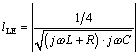
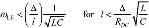
The mathematical extent of the lumped-element region includes all combinations of w and l for which the magnitude of the propagation coefficient l g ( w ) remains less than D .
Equation 3.22

|
where |
D is an arbitrary constant typically set to about 1/4. |
|
l is the length of the transmission line, m, and |
|
|
g ( w ) is the propagation coefficient of the transmission line (complex neper/m) at frequency w (rad/s). |
For typical digital transmission applications the quantity g ( w ) increases monotonically from DC so that inequality [3.22] need be checked only at the maximum length and maximum anticipated frequency of operation. If the transmission line satisfies [3.22] at that maximum point, it will similarly satisfy [3.22] at all shorter lengths and lower frequencies.
Beware the fallacy that a short transmission line, even one short enough to fall into the lumped-element region, never requires termination. Such is not the case. Even a perfect zero-length transmission line may resonate horribly if used to interconnect a ferociously reactive combination of source and load (see Section 3.4.6, "Step Response (Lumped-Element Region)").
The classification of a transmission line in the lumped-element region does not determine how the line is going to act. It determines merely how the line may be analyzed .
POINT TO REMEMBER
- The classification of a transmission line in the lumped-element region does not determine how the line is going to act. It determines merely how the line may be analyzed.
3.4.1 Boundary of Lumped-Element Region
A exact physical interpretation of equation [3.22] is fairly difficult to comprehend; however, by making a few reasonable assumptions you may approximate the boundary of the lumped-element region in the following way. First assume that the propagation coefficient for a transmission line is given by [3.13], and that parameters R, L , and C are constants that do not much vary with frequency. Substituting [3.13] for the propagation coefficient in [3.22], you may derive the following equation relating w and l LE .
Equation 3.23
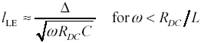
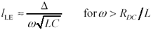
Since the boundaries of the lumped-element region is by definition a rather fuzzy concept in the first place, you needn't bother with precise calculation of [3.23], substituting instead two asymptotic approximations that handle the cases where j w L is either much smaller than, or much larger than, R . These are the boundaries drawn in Figure 3.2.
Equation 3.24
Equation 3.25
|
where |
w is frequency of operation, rad/s, |
|
R DC is the series DC resistance of the transmission line (signal and return resistances added together), W /m, |
|
|
L is the transmission-line series inductance per meter, H/m, |
|
|
C is the transmission-line shunt capacitance per meter, F/m, |
|
|
l LE is the upper boundary of the lumped-element region, m, and |
|
|
D is an arbitrary constant customarily set to 1/4. |
|
|
NOTE: |
For differential configurations, define R DC as the sum of the resistances of the outbound and returning conductors, and L and C as the inductance and capacitance respectively of the differential transmission line thus formed , L = Z DIFFERENTIAL / v DIFFERENTIAL and C = 1/( Z DIFFERENTIAL · v DIFFERENTIAL ). |
If the length l is known and you wish to determine the maximum frequency of lumped-element operation, the constraints in [3.24] and [3.25] may be inverted to produce
Equation 3.26
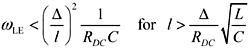
Equation 3.27
Here you can see the value of the approximations used in [3.24] and [3.25], as the direct inversion of any equation utilizing the full, frequency-varying form of g ( w ) would indeed be a formidable undertaking.
In physical terms, constraint [3.24] asks that the RC time constant l 2 R DC C formed by the structure's DC resistance and capacitance remain far smaller than the time constant 1/ w associated with the highest frequency of operation. Constraint [3.25] asks that the LC delay of the transmission structure  remain much shorter than 1/ w . Working together, these two constraints ensure that the delay internal to the transmission structure itself remains far smaller than the signal rise or fall time. Under these conditions the transmission line enjoys a peculiarly tight coupling between the source and load impedances. When connecting obnoxiously reactive components , the system can still exhibit vigorous amounts of simple harmonic resonance , but what it cannot do is create the sort of lingering, unexpectedly late reflections that happen on a truly distributed circuit.
Transmission lines short enough to operate in the lumped-element region rarely require termination except in unusual situations involving very low-impedance drivers coupled either through exorbitant amounts of packaging inductance or connected through transmission lines to heavily reactive loads.
POINT TO REMEMBER
- A transmission line can always be shortened to a length below which it operates in the lumped-element region.
- Transmission lines short enough to operate in the lumped-element region rarely require termination.
3.4.2 Pi Model
The pi-model circuit approximates the behavior of a short transmission line (Figure 3.4). This circuit is equivalent to a second-order Taylor series solution of the transmission equations (see Appendix D, "Accuracy of Pi Model").
Figure 3.4. The pi model applies to any transmission line electrically short compared to the signal wavelength, and where the time constant l 2 R DC C remains small compared to the signal period.
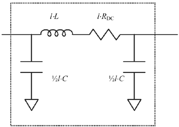
The name pi model derives from the schematic configuration of the three circuit elements in the model whose positions resemble the three strokes of the Greek letter p .
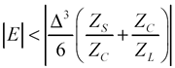
Over the domain prescribed by [3.22], the fractional accuracy E of predictions made by the pi model is approximately bounded by
Equation 3.28
|
where |
Z S , Z C , and Z L represent the source impedance of the driver, the characteristic impedance of the transmission line, and the impedance of the load respectively. |
|
In typical cases where the ratios Z S / Z C and Z C / Z L each remain less than two and |
|
|
D = 1/4 the accuracy is better than 1% (see Appendix D). |
|
Those experienced in analog design may be concerned that the inductive and capacitive components of the pi model could under some circumstances resonate severely. If you have made this discovery I should like to congratulate you on your astute observation and also address your discomfort by pointing out that condition [3.27] precludes the realization of such resonance by restricting the range of applicability of the model to only those frequencies well below the resonant frequency.
POINT TO REMEMBER
- The pi model applies to any transmission line electrically short compared to the signal wavelength, and where the time constant l 2 R DC C remains small compared to the signal period.
3.4.3 Taylor-Series Approximation of H (Lumped-Element Region)
Operation within the lumped-element region assumes a line delay short compared to the rise and fall time of the externally applied signals. Both source and load therefore exert an almost instantaneous influence over the system behavior, creating the illusion of a direct connection between the two. Keep in mind, though, that even on a short line two fully independent modes of propagation still exist (out and back). Equations [3.13] through [3.17] still apply (see Section 3.2.1, "A Transmission Line Is Always a Transmission Line").
Within the lumped-element region the limited magnitude of the propagation coefficient l g renders possible the use of Taylor-series expansions for H and H “1 in this region. These expansions greatly simplify the analysis.
Equation 3.29
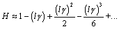
Equation 3.30
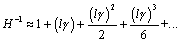
|
where |
H is the one-way propagation function of the transmission line (a complex, dimensionless quantity), |
|
l is the transmission-line length (m), and |
|
|
g is the per-unit-length propagation coefficient (complex neper/m). |
Calculations of circuit behavior made using the Taylor-series approximation depend only upon ordinary differential equations as opposed to the partial differential equations required to construct a fully distributed model. Therein lies one advantage of operation in the lumped-element region ”it's relatively easy to determine in this region how a transmission line will respond.
This text uses only the first four terms of the Taylor-series expansion to generate the following approximations used in calculation of lumped-element input impedance and system gain.
Equation 3.31
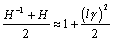
Equation 3.32
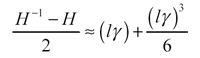
|
where |
H is the one-way propagation function of the transmission line (a complex, dimensionless quantity), |
|
l is the transmission-line length (m), and |
|
|
g is the per-unit-length propagation coefficient (complex neper/m). |
POINT TO REMEMBER
- Within the lumped-element region you may use Taylor-series expansions for H and H “1 .
3.4.4 Input Impedance (Lumped-Element Region)
On a lumped-element line the load exerts an almost instantaneous influence over the input impedance of the structure (see Section 3.2.1, "A Transmission Line Is Always a Transmission Line").
This happens because, by definition, the transit delay of a lumped-element structure is limited to a short fraction of the signal risetime. In the time the signal progresses only partway through a transition, information about the changing input propagates to the far end of the line, interacts with the load, and reflects back to the source. The source therefore receives almost instantaneous feedback about the conditions at the load.
On very long lines the same general scenario applies with the exception that the longer transit delay effectively disconnects the source and load in a temporal sense. Information about the load reflects back to the source too late to affect the progress of an individual rising or falling edge. The reflection in such a case, rather than being considered part of the "input impedance" of the line, may be considered separately as a distinct "reflection." From a mathematical viewpoint, whether you consider the reflection as a perturbation in the input impedance of the structure or as a structurally distinct reflection from a distant load makes no difference, provided that you properly account for the reflected-wave effect somehow in your calculations.
Let's next examine the input impedance of a lumped-element structure under various conditions of loading. To begin, apply the lumped-element Taylor-series approximations [3.31] and [3.32] to the general equation for input impedance [3.16], neglecting all but the constant and linear terms.
Equation 3.33
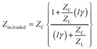
Assuming the line to be very lightly loaded ( Z L >> Z C ) causes the right-hand terms in the numerator and denominator to vanish , leaving you with a very simple expression for the input impedance.
Equation 3.34
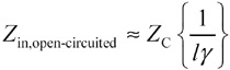
Plugging in the definitions of g [3.13] and Z C [3.15] reveals a classic result ”that the input impedance of a short, unloaded transmission line looks entirely capacitive.
Equation 3.35
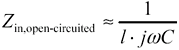
The amount of capacitance equals the total distributed capacitance ( lC ) of the line. The approximately equal sign in [3.35] exists to remind you that this equation applies only under very special circumstances:
- The line delay is short compared to the signal rise/fall time (perhaps 1/6 or at most no more than 1/3 of the rise/fall time).
- The line is lightly loaded at its endpoint.
Violation of either constraint invalidates [3.35]. I mention this because one of the most widely held misconceptions about transmission lines is the belief that the input impedance of a transmission line looks capacitive. It holds this appearance only when short enough to qualify as a lumped-element structure and when lightly loaded. Under other conditions the input impedance varies considerably.
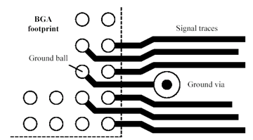
For example, let's see what happens if the line is short-circuited to ground at the far end. You may be asking yourself, What good is a transmission line shorted at the far end? The application for such a line is the grounding of an integrated circuit (IC) pin on a PC layout that does not permit room for a ground via contiguous with the IC pin pad. In congested situations it is common for (inexperienced) layout persons to connect the IC ground pin with a short trace to a ground via (see Figure 3.5). The following discussion computes the effective input impedance of the trace leading to ground, as viewed from the perspective of the IC ground ball.
Figure 3.5. This ground via lies too far from the ball-grid array (BGA) ground ball.
Assuming the line to be shorted to ground at the ground via implies that ( Z L << Z C ). This assumption inflates the right-hand terms in both numerator and denominator of [3.33], causing them to dominate the equation and leaving you with this simple expression for the input impedance.
Equation 3.36
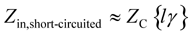
Again plugging in definitions [3.13] and [3.15] reveals that the input impedance of a short, grounded transmission line looks either inductive or resistive, depending on the ratio of j w L to R .
Equation 3.37
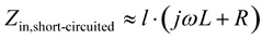
Equation [3.37] tells you that the input impedance of a short line shorted to ground at the far end looks like nothing more or less than the total series impedance, inductive plus resistive, of the structure. Formula [3.37] provides the basis for making calculations of the ground-bounce (also called simultaneous switching noise ) generated when a current i ( t ) passes through a short trace leading to ground.
At the frequencies associated with most high-speed digital grounding problems, the inductance of a pcb trace is almost always much more significant than the resistance, leading to this simplified conclusion:
The input impedance of a short, grounded pcb trace looks entirely inductive .
The amount of inductance equals the total distributed inductance ( lL ) of the transmission line formed by the pcb trace and its associated return path . The approximately equal sign in [3.37] exists to remind you that this equation applies only under very special circumstances:
- The line delay is short compared to the signal rise/fall time (perhaps 1/6 or at most no more than 1/3 of the rise/fall time).
- The line is grounded at its endpoint.
You should check [3.33] to verify that when the line is properly terminated ( Z L = Z C ) the numerator and denominator return the same result so that the effective input impedance of the structure equals precisely Z C . This is the situation on an end-terminated transmission line as typically implemented on a pcb.
I am compelled to point out that for lines operated at frequencies below the onset of the LC region, the input impedance Z C ( w ) is not at all constant but a strongly frequency-varying quantity with a phase angle of 45 degrees. Accurately matching the impedance Z C in this region is not a trivial exercise. Fortunately, lines short enough to qualify for lumped-element analysis hardly require termination.
POINTS TO REMEMBER
- The input impedance of a short, unloaded transmission line looks entirely capacitive.
- The input impedance of a short, grounded pcb-trace looks entirely inductive.
3.4.5 Transfer Function (Lumped-Element Region)
Substitute expressions [3.31] and [3.32] into [3.17] to compute the overall circuit gain G .
Equation 3.38
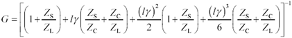
From [3.38] you can (given sufficient mental effort) deduce the conditions necessary to achieve gain flatness . To begin your investigation of this equation, observe that as the term l g approaches zero it renders negligible all the terms associated with various powers of l g . The propagation function G in that case asymptotically approaches Z L /( Z S + Z L ), precisely the transfer gain you would expect if the source and load were directly connected. This simple mathematical deduction indicates that as the length l of the line is foreshortened, eventually you come to a length so short that the transmission line exerts no observable influence over the outcome ”the response at that point depends only on the configuration of source and load. In other words,
Any transmission line can be shortened to the point where it acts as a perfect connection .
Another conclusion you might draw from the analysis so far is that the gain Z L /( Z S + Z L ) is in some sense the best you can do given the source and load. No directly attached configuration of transmission lines will be able to improve on this response. A corollary to this principle is simply stated:
If the source can't drive the load in the first place, then hooking the source and load together with a transmission line isn't likely to make things better .
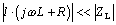
Within the lumped element region you may assume the extent x of the line is set to a value such that the magnitude of the coefficient l g remains less than D = 1/4 at all frequencies of interest. Under such an assumption you might reasonably expect to ignore the second- and third-order terms in [3.38], but you could hardly ignore the first-order term, particularly if either of the ratios Z S / Z C or Z C / Z L exceeds unity. This observation may be cast into a statement of the conditions under which the wiring exerts negligible influence over the connection of source and load.
Equation 3.39

Equation 3.40

Equation 3.41

Conditions [3.39] through [3.41] may be simplified and perhaps made more recognizable by inserting the definitions of g [3.13] and Z C [3.15].
Equation 3.42

Equation 3.43
Formulas [3.42] and [3.43] stipulate the two conditions that are required above and beyond [3.41] such that the line not exert any deleterious influence over signal quality, namely,
- The source impedance of the driver must be far less than the impedance represented by the total shunt capacitance 1/( l · j w C ) of the line [3.42], and
- The total series impedance of the line l · ( j w L + R ) must remain far less than the impedance of the load [3.43].
If either condition is not satisfied, then the presence of the transmission line may substantially affect the signal amplitude and/or quality.
In the event the line is driven by an ideal voltage source ( Z S = 0) and coupled to an ideal load at the endpoint ( Z L =  ), equation [3.38] reduces to this form:
Equation 3.44
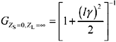
Equation [3.44] provides a direct relationship between the definition of the lumped-element boundary l g < D and the circuit performance expected under ideal conditions. Given D = 0.25, the unloaded gain of the transmission line at the lumped-element boundary can differ from unity by no more than D 2 /2 = .032. Beware that the appearance of good performance with ideal loading does not imply that the transmission line would achieve satisfactory performance under other conditions of loading.
It is usually sufficient to check the conditions [3.39] through [3.41] at the highest anticipated frequency of operation. For digital circuits, that frequency corresponds to w knee . If the circuit performs satisfactorily at w knee , then conditions will generally improve at lower frequencies, provided that the following conditions are met:
- The propagation coefficient g increases monotonically with frequency [3.41].
- Z S may act in a capacitive manner (increasing at lower frequencies) as long as it does so no faster than 1/ w . This condition implies that Z S contain no parallel resonance at frequencies less than w knee . In ordinary digital circuits Z S is inductive and tending rapidly towards zero at DC, so that if [3.42] is met at w knee , then the inequality improves quadratically as w tends to zero.
- Z L may act in an inductive manner ( decreasing at lower frequencies) as long as it does so no faster than j w L + R . This condition places restrictions on the type and configuration of inductive loads that may be satisfactorily driven by a lumped-element transmission line. In ordinary digital circuits Z L is capacitive and tending to infinity at DC, so that if [3.43] is met at any particular frequency w 1 , the inequality improves as 1/ w 2 when w is reduced from w 1 to w LC and then inversely with w for w below w LC .
Taken together, the preceding three conditions suggest that any ordinary transmission line that is satisfactorily terminated for operation at frequencies at the lumped-element boundary will also work satisfactorily at frequencies within the lumped-element region. This principle should relieve you of certain worries about the peculiar way in which the transmission-line impedance spikes to infinity near DC. Even when Z C goes to infinity, as long as conditions [3.19] through [3.41] are met, the circuit will still function.
POINTS TO REMEMBER
- Any transmission line can be shortened to the point where it acts as a perfect connection.
- If the source can't drive the load in the first place, then hooking the source and load together with a transmission line isn't likely to make things better.
- Conditions necessary such that a short, lumped-element transmission line not affect signal quality are given by [3.39] through [3.41].
3.4.6 Step Response (Lumped-Element Region)
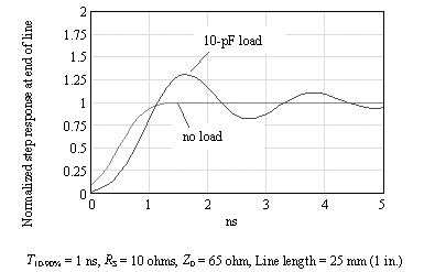
The best way to illustrate the general effect of a lumped-element transmission line is by example (Figure 3.6).
Figure 3.6. This short trace meets the conditions for a lumped-element circuit, yet when loaded with 10 pF it rings horribly.
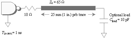
Driver
- Risetime: 1 ns
- Output impedance: 10 ohms (shown explicitly as a 10- W resistor)
- Operating frequency (corresponds to center of spectral lobe associated with each rising or falling edge): w edge = 2 p (.35)/ t r = 2.2 ·10 9 rad/s
Transmission line
- Characteristic impedance: Z = 65 ohm (microstrip)
- Length: 25 mm (1 in.)
- Effective dielectric constant: 3.8
- High-frequency propagation velocity:
- DC resistance: 3 W /m
Load
- When present, a 10-pF capacitive load
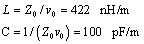
From the high-frequency values of Z and v you can determine the transmission line parameters L and C :
Equation 3.45
Presuming that the inductive effect of the line far outweighs the resistance (in this case it does), you may approximate the magnitude of the propagation coefficient using only the inductive term.
Equation 3.46
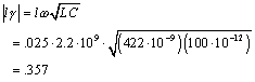
This value of the propagation coefficient puts you just outside the official boundary of the lumped-element region at a point where you should expect the pi-model approximations (and indeed equation [3.38]) to be accurate only to about 3%.
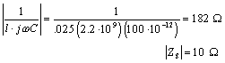
Next check conditions [3.42] and [3.43] to see whether the line significantly influences signal quality. Condition [3.42] appears to be satisfied.
Equation 3.47
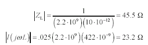
Checking [3.43] for the case of no load capacitance (infinite Z L ), you can see that it is clearly true as well ”leading to the important conclusion that for rise and fall times no faster than 1 ns, this microstrip in the absence of a load induces practically no distortion in the transmitted waveform.
Re-checking [3.43] for the case of a 10-pF load capacitance leads to an opposite conclusion. In this case Z L exceeds the series impedance of the line by but a small amount (a factor of only 2:1) implying that the transmission line will have a noticeable effect on the shape of the received signal.
Equation 3.48
Indeed, when the received waveform is plotted under the two conditions, showing the outcome with no load and with a 10-pF load, the unloaded condition shows an undistorted outcome, while the 10-pF load displays prodigious amounts of ringing (Figure 3.7).
Figure 3.7. Even a short transmission line displays prodigious amounts of ringing when combined with a low-impedance driver and a heavy capacitive load.
Those readers steeped in the art of analog design may find some satisfaction in comparing this result with the simple pi-model approximation (Figure 3.4). The values for inductance and capacitance in that figure are
Equation 3.49
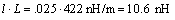
Equation 3.50
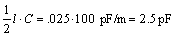
When driven by a low-impedance source, the capacitor on the left in Figure 3.4 plays only a small role in determining the result. The main effect is an R-L-C series-resonant circuit formed by the output resistance of the driver, the 10.6 nH series inductance, and the 2.5 pF capacitor on the right, which connects in parallel with the load .
In an unloaded state the resonant frequency w res associated with the inductive and capacitive components lies far above the bandwidth of the driver.
Equation 3.51
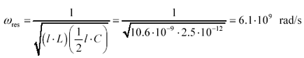
An R-L-C resonance certainly exists at 6.1 Grad/s, but since this is well above the spectral center of gravity of the rising and falling edges coming out of the driver (2.2 Grad/s), you never see it. Condition [3.41] ensures that under lightly loaded conditions the line is always sufficiently short to guarantee the resonance falls above the frequency of operation.
With a 10-pF load applied, the situation changes. The new load capacitance swells the total amount of capacitance on the right side of the pi model, reducing the resonant frequency to within a stone's throw of the bandwidth of the driver. In this example the new resonant frequency is a function of the series inductance of the line (10.6 nH) and the parallel combination of 2.5 pF and 10 pF.
Equation 3.52
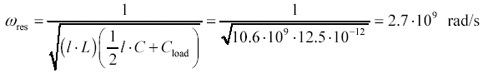
Such a resonance should have a period of 2 p /(2.7 ·10 9 ) = 2.3 ns, corresponding nicely to the ringing period displayed in Figure 3.7.
POINT TO REMEMBER
- Even a short transmission line may resonate horribly if used to interconnect a ferociously reactive combination of source and load.
Fundamentals
- Impedance of Linear, Time-Invariant, Lumped-Element Circuits
- Power Ratios
- Rules of Scaling
- The Concept of Resonance
- Extra for Experts: Maximal Linear System Response to a Digital Input
Transmission Line Parameters
- Transmission Line Parameters
- Telegraphers Equations
- Derivation of Telegraphers Equations
- Ideal Transmission Line
- DC Resistance
- DC Conductance
- Skin Effect
- Skin-Effect Inductance
- Modeling Internal Impedance
- Concentric-Ring Skin-Effect Model
- Proximity Effect
- Surface Roughness
- Dielectric Effects
- Impedance in Series with the Return Path
- Slow-Wave Mode On-Chip
Performance Regions
- Performance Regions
- Signal Propagation Model
- Hierarchy of Regions
- Necessary Mathematics: Input Impedance and Transfer Function
- Lumped-Element Region
- RC Region
- LC Region (Constant-Loss Region)
- Skin-Effect Region
- Dielectric Loss Region
- Waveguide Dispersion Region
- Summary of Breakpoints Between Regions
- Equivalence Principle for Transmission Media
- Scaling Copper Transmission Media
- Scaling Multimode Fiber-Optic Cables
- Linear Equalization: Long Backplane Trace Example
- Adaptive Equalization: Accelerant Networks Transceiver
Frequency-Domain Modeling
- Frequency-Domain Modeling
- Going Nonlinear
- Approximations to the Fourier Transform
- Discrete Time Mapping
- Other Limitations of the FFT
- Normalizing the Output of an FFT Routine
- Useful Fourier Transform-Pairs
- Effect of Inadequate Sampling Rate
- Implementation of Frequency-Domain Simulation
- Embellishments
- Checking the Output of Your FFT Routine
Pcb (printed-circuit board) Traces
- Pcb (printed-circuit board) Traces
- Pcb Signal Propagation
- Limits to Attainable Distance
- Pcb Noise and Interference
- Pcb Connectors
- Modeling Vias
- The Future of On-Chip Interconnections
Differential Signaling
- Differential Signaling
- Single-Ended Circuits
- Two-Wire Circuits
- Differential Signaling
- Differential and Common-Mode Voltages and Currents
- Differential and Common-Mode Velocity
- Common-Mode Balance
- Common-Mode Range
- Differential to Common-Mode Conversion
- Differential Impedance
- Pcb Configurations
- Pcb Applications
- Intercabinet Applications
- LVDS Signaling
Generic Building-Cabling Standards
- Generic Building-Cabling Standards
- Generic Cabling Architecture
- SNR Budgeting
- Glossary of Cabling Terms
- Preferred Cable Combinations
- FAQ: Building-Cabling Practices
- Crossover Wiring
- Plenum-Rated Cables
- Laying Cables in an Uncooled Attic Space
- FAQ: Older Cable Types
100-Ohm Balanced Twisted-Pair Cabling
- 100-Ohm Balanced Twisted-Pair Cabling
- UTP Signal Propagation
- UTP Transmission Example: 10BASE-T
- UTP Noise and Interference
- UTP Connectors
- Issues with Screening
- Category-3 UTP at Elevated Temperature
150-Ohm STP-A Cabling
- 150-Ohm STP-A Cabling
- 150- W STP-A Signal Propagation
- 150- W STP-A Noise and Interference
- 150- W STP-A: Skew
- 150- W STP-A: Radiation and Safety
- 150- W STP-A: Comparison with UTP
- 150- W STP-A Connectors
Coaxial Cabling
- Coaxial Cabling
- Coaxial Signal Propagation
- Coaxial Cable Noise and Interference
- Coaxial Cable Connectors
Fiber-Optic Cabling
- Fiber-Optic Cabling
- Making Glass Fiber
- Finished Core Specifications
- Cabling the Fiber
- Wavelengths of Operation
- Multimode Glass Fiber-Optic Cabling
- Single-Mode Fiber-Optic Cabling
Clock Distribution
- Clock Distribution
- Extra Fries, Please
- Arithmetic of Clock Skew
- Clock Repeaters
- Stripline vs. Microstrip Delay
- Importance of Terminating Clock Lines
- Effect of Clock Receiver Thresholds
- Effect of Split Termination
- Intentional Delay Adjustments
- Driving Multiple Loads with Source Termination
- Daisy-Chain Clock Distribution
- The Jitters
- Power Supply Filtering for Clock Sources, Repeaters, and PLL Circuits
- Intentional Clock Modulation
- Reduced-Voltage Signaling
- Controlling Crosstalk on Clock Lines
- Reducing Emissions
Time-Domain Simulation Tools and Methods
- Ringing in a New Era
- Signal Integrity Simulation Process
- The Underlying Simulation Engine
- IBIS (I/O Buffer Information Specification)
- IBIS: History and Future Direction
- IBIS: Issues with Interpolation
- IBIS: Issues with SSO Noise
- Nature of EMC Work
- Power and Ground Resonance
Points to Remember
Appendix A. Building a Signal Integrity Department
Appendix B. Calculation of Loss Slope
Appendix C. Two-Port Analysis
- Appendix C. Two-Port Analysis
- Simple Cases Involving Transmission Lines
- Fully Configured Transmission Line
- Complicated Configurations
Appendix D. Accuracy of Pi Model
Appendix E. erf( )
Notes
EAN: N/A
Pages: 163
