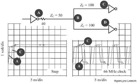
Driving Multiple Loads with Source Termination
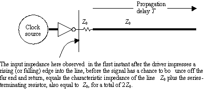
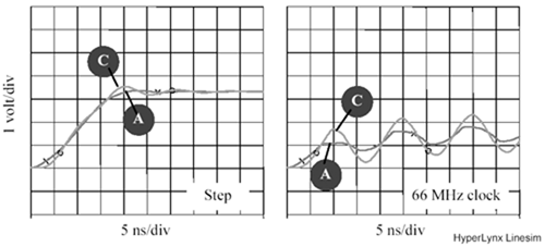
Figure 12.33 shows that in the first instant after the driver impresses a rising (or falling) edge into a source- terminated configuration, before the signal has a chance to bounce off the far end and return, the input impedance equals twice the characteristic impedance of the line. Not only that, the drive current requirement drops to zero after 2 T seconds, lowering the average power drain. These facts may tempt you to assume that a single gate designed to drive a single end-terminated configuration should be able to drive multiple (at least) source-terminated lines. That assumption is incorrect.
A careful examination of initial conditions, however, reveals that the peak drive current i PEAK for the source- and end-terminated lines are the same. For example, in Figure 12.33 the i PEAK required to initiate a full- sized rising edge into an impedance of 2 Z is V CC /2 Z .
Figure 12.33. The drive current required to initiate a full-sized rising edge at the end of the line is therefore V CC /2 Z .
An end-terminated example, assuming the end terminator is symmetrically split , may be analyzed using the Thevenin equivalent circuit of Figure 12.23. In the Thevenin equivalent circuit, because the battery is biased at the midpoint , the driver need only provide enough current to change the voltage at the input to R T by half of V CC in either direction. The i PEAK required is thus (1/2;)V CC / Z , precisely the same peak current required by the series terminator.
If your driver cannot pump out the required amount of current, then your initial rising edge at the receiver won't be full sized. Note that in the series-terminated case the driver does not have to meet V OH at the stipulated peak current, but you must know with some degree of precision what voltage your driver is guaranteed to produce when sourcing i PEAK . Given the voltage produced at the required i PEAK , the external series-terminating resistor is then sized to produce a voltage drop precisely equal to the difference between the driver output voltage at current i PEAK and the initial required voltage on the line, which is half of V CC . If the resistor is sized properly, the voltage-doubling effect at the unterminated far end of the line will ultimately bring the initial rising edge of the received signal up to exactly full value.
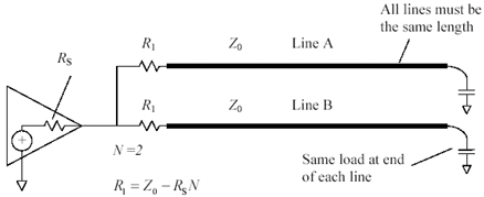
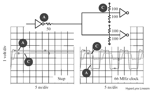
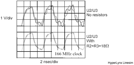
Some driver circuits can easily source enough current to drive two source-terminated lines. Is it possible to drive two or more source-terminated lines from such a driver? Yes, but only under the limited conditions diagramed in Figure 12.34.
Figure 12.34. A single driver can drive multiple source-terminated loads only under restricted conditions.
The trick to understanding this figure is to realize that the lines are coupled together into a jointly resonant structure. You cannot properly analyze just one line without seeing what happens to all the lines. The coupling happens because of the finite output impedance of the driver.
If the driver output impedance R S were zero (it never is), there would be no cross-coupling between lines, and you could simply use a separate series-terminating resistor of value R 1 = Z on each line. Unfortunately, the reality of finite driver impedance forces us to contemplate joint resonance . The paragraphs below show how to jointly analyze the system.
Skipping ahead to the answer, multiple source termination with a nonzero driver impedance works only if the lines are equally long and the loads at each end are balanced . The source-termination resistors must equal
Equation 12.6

|
where |
R S = output resistance of driver, W , |
|
Z = transmission line characteristic impedance, W , |
|
|
R 1 = value of resistance added to each trace, and |
|
|
N = number of driven lines. |
When driving one line ( N = 1), [12.6] matches the total source impedance ( R S + R 1 ) to the characteristic impedance Z . This is a normal source termination. When driving multiple lines, [12.6] prescribes smaller source-terminating resistors. With N too large, [12.6] goes negative, implying that no practical solution exists.
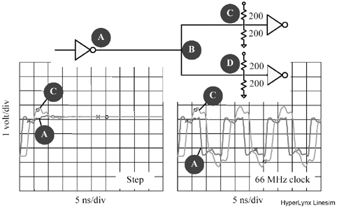
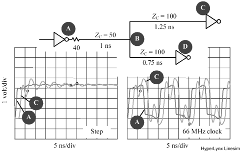
Let's analyze the lines in Figure 12.34 one at a time to see what happens. In Figure 12.34, a pulse travels down line A toward the load. This pulse reflects off the far end of line A, returning to the driver. In the usual application of source termination, the source termination matches the characteristic impedance of the line, eliminating the reflection at the driver. In Figure 12.34, however, the effective source impedance is not matched; it is set slightly lower than the characteristic impedance of the line. The returning pulse on line A therefore bounces off the driver, producing a negative reflection. So far, the negative reflection looks like a problem.
Another effect occurs at the same time. As current from the returning pulse on line A surges into the driver chip and through R S , it generates a voltage at the driver output pin. This voltage couples into line B. The polarity of the crosstalk pulse coupled onto line B is positive.
So far, the consequences of the returning reflected pulse on line A seem to include a negative reflection on line A and a positive crosstalk pulse on line B.
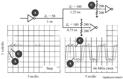
Now imagine what happens if the returning signals reflected off the far ends of lines A and B arrive at the same time. Each signal will induce on its own line a negative reflection and on the other line a positive amount of crosstalk. If you choose the resistor values carefully (according to [12.6]), you can get the negative reflection and positive crosstalk to cancel exactly. The result is a perfectly damped system.
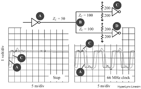
The conditions under which perfect cancellation may be achieved are very restrictive :
- The lines must be equally long (this guarantees the reflected pulses will arrive at the same time).
- The loads must be balanced (this guarantees the reflected pulses will have the same shape).
- The resistors must be calculated according to [12.6].
Equation [12.6] sets the source-terminating resistance so that line A experiences a negative reflection pulse exactly compensated for by the positive crosstalk pulse from line B. Equation [12.6] works with any number of lines, as long as they are equal in length and identically loaded.
Perfect balance rarely occurs in practice. If the lines are not perfectly balanced, the reflections and crosstalk from each line will not cancel. Incomplete cancellation makes the system ring.
POINT TO REMEMBER
- A single driver can service two or more source-terminated lines only under limited conditions.
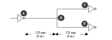
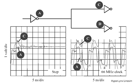
12.9.1 To Tee or Not To Tee
POINTS TO REMEMBER
- A slow driver can damp ringing, but it may need to be too slow for your circuit.
- Appropriately placed attenuating networks can damp all the oscillatory modes at the expense of shrinking the received signal.
- A weak termination can help reduce, but totally cure, overshoot and ringing.
- Test all combinations of maximum and minimum load capacitance and line length.
- Eventually, someone will inherit your hairball design and try to figure out what you did. Keep it simple.
12.9.2 Driving Two Loads
POINT TO REMEMBER
- Hidden within every split-tee network is an unconstrained resonance.
Fundamentals
- Impedance of Linear, Time-Invariant, Lumped-Element Circuits
- Power Ratios
- Rules of Scaling
- The Concept of Resonance
- Extra for Experts: Maximal Linear System Response to a Digital Input
Transmission Line Parameters
- Transmission Line Parameters
- Telegraphers Equations
- Derivation of Telegraphers Equations
- Ideal Transmission Line
- DC Resistance
- DC Conductance
- Skin Effect
- Skin-Effect Inductance
- Modeling Internal Impedance
- Concentric-Ring Skin-Effect Model
- Proximity Effect
- Surface Roughness
- Dielectric Effects
- Impedance in Series with the Return Path
- Slow-Wave Mode On-Chip
Performance Regions
- Performance Regions
- Signal Propagation Model
- Hierarchy of Regions
- Necessary Mathematics: Input Impedance and Transfer Function
- Lumped-Element Region
- RC Region
- LC Region (Constant-Loss Region)
- Skin-Effect Region
- Dielectric Loss Region
- Waveguide Dispersion Region
- Summary of Breakpoints Between Regions
- Equivalence Principle for Transmission Media
- Scaling Copper Transmission Media
- Scaling Multimode Fiber-Optic Cables
- Linear Equalization: Long Backplane Trace Example
- Adaptive Equalization: Accelerant Networks Transceiver
Frequency-Domain Modeling
- Frequency-Domain Modeling
- Going Nonlinear
- Approximations to the Fourier Transform
- Discrete Time Mapping
- Other Limitations of the FFT
- Normalizing the Output of an FFT Routine
- Useful Fourier Transform-Pairs
- Effect of Inadequate Sampling Rate
- Implementation of Frequency-Domain Simulation
- Embellishments
- Checking the Output of Your FFT Routine
Pcb (printed-circuit board) Traces
- Pcb (printed-circuit board) Traces
- Pcb Signal Propagation
- Limits to Attainable Distance
- Pcb Noise and Interference
- Pcb Connectors
- Modeling Vias
- The Future of On-Chip Interconnections
Differential Signaling
- Differential Signaling
- Single-Ended Circuits
- Two-Wire Circuits
- Differential Signaling
- Differential and Common-Mode Voltages and Currents
- Differential and Common-Mode Velocity
- Common-Mode Balance
- Common-Mode Range
- Differential to Common-Mode Conversion
- Differential Impedance
- Pcb Configurations
- Pcb Applications
- Intercabinet Applications
- LVDS Signaling
Generic Building-Cabling Standards
- Generic Building-Cabling Standards
- Generic Cabling Architecture
- SNR Budgeting
- Glossary of Cabling Terms
- Preferred Cable Combinations
- FAQ: Building-Cabling Practices
- Crossover Wiring
- Plenum-Rated Cables
- Laying Cables in an Uncooled Attic Space
- FAQ: Older Cable Types
100-Ohm Balanced Twisted-Pair Cabling
- 100-Ohm Balanced Twisted-Pair Cabling
- UTP Signal Propagation
- UTP Transmission Example: 10BASE-T
- UTP Noise and Interference
- UTP Connectors
- Issues with Screening
- Category-3 UTP at Elevated Temperature
150-Ohm STP-A Cabling
- 150-Ohm STP-A Cabling
- 150- W STP-A Signal Propagation
- 150- W STP-A Noise and Interference
- 150- W STP-A: Skew
- 150- W STP-A: Radiation and Safety
- 150- W STP-A: Comparison with UTP
- 150- W STP-A Connectors
Coaxial Cabling
- Coaxial Cabling
- Coaxial Signal Propagation
- Coaxial Cable Noise and Interference
- Coaxial Cable Connectors
Fiber-Optic Cabling
- Fiber-Optic Cabling
- Making Glass Fiber
- Finished Core Specifications
- Cabling the Fiber
- Wavelengths of Operation
- Multimode Glass Fiber-Optic Cabling
- Single-Mode Fiber-Optic Cabling
Clock Distribution
- Clock Distribution
- Extra Fries, Please
- Arithmetic of Clock Skew
- Clock Repeaters
- Stripline vs. Microstrip Delay
- Importance of Terminating Clock Lines
- Effect of Clock Receiver Thresholds
- Effect of Split Termination
- Intentional Delay Adjustments
- Driving Multiple Loads with Source Termination
- Daisy-Chain Clock Distribution
- The Jitters
- Power Supply Filtering for Clock Sources, Repeaters, and PLL Circuits
- Intentional Clock Modulation
- Reduced-Voltage Signaling
- Controlling Crosstalk on Clock Lines
- Reducing Emissions
Time-Domain Simulation Tools and Methods
- Ringing in a New Era
- Signal Integrity Simulation Process
- The Underlying Simulation Engine
- IBIS (I/O Buffer Information Specification)
- IBIS: History and Future Direction
- IBIS: Issues with Interpolation
- IBIS: Issues with SSO Noise
- Nature of EMC Work
- Power and Ground Resonance
Points to Remember
Appendix A. Building a Signal Integrity Department
Appendix B. Calculation of Loss Slope
Appendix C. Two-Port Analysis
- Appendix C. Two-Port Analysis
- Simple Cases Involving Transmission Lines
- Fully Configured Transmission Line
- Complicated Configurations
Appendix D. Accuracy of Pi Model
Appendix E. erf( )
Notes
EAN: N/A
Pages: 163
