Signal Integrity Simulation Process
A good simulator is a predictive tool, and good predictions don't come easily. The process involves a lot of steps, each one of which controls the efficacy of the overall result.
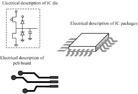
Signal integrity simulation at the pcb level begins with electrical descriptions of the IC die involved, the IC packages, and the traces on the pcb (Figure 13.1). The objective at this stage is to capture a reasonable description of the components involved, a description sufficiently accurate to permit good-quality simulations, and yet not so complicated that it becomes difficult to manage. The process of distilling from the plethora of available data those pieces of information most relevant to the modeling task at hand is called parameter extraction .
Figure 13.1. Signal integrity simulation at the pcb level begins with electrical descriptions of the IC die involved, the IC packages, and the traces on the pcb.

For an individual IC die, one extracts parameters relevant to the operation of the I/O circuits. These parameters may be rendered in the form of a SPICE circuit description file or (more appropriate for large-scale simulation) an IBIS specification file.
Prediction is very difficult, especially about the future.
”Neils Bohr

For a chip package, one begins with a physical description and extracts from it information about the mutual inductance and capacitance between every pair of pins. For small packages, this information may be encoded in the form of two matrices of mutual coupling terms (one for inductance and one for capacitance ) plus a resistance vector (one value per pin). For larger packages (or at extremes of speed), the coupling information may be represented as a collection of coupled transmission line models interconnected by mutual-coupling coefficients.
At the board level, one extracts a collection of trace impedances, trace lengths, trace topologies, and coupling functions representing all traces and connectors.
The set of all electrical models for the chips, packages, and traces on a pcb constitutes , for signal integrity purposes, a complete electrical model of the board. The most common errors arising at this stage are:
- Choosing an inappropriate degree of modeling for the problem at hand, or
- Goofing up the data entry, assigning incorrect or out-of-date values to parameters.
In the first case a model that is too simplistic will gloss over the fine details, often missing important aspects of system performance. On the other hand, a model that is overly complex will take so long to put together that you may never finish it. Finding the right balance is a matter of experience.
The problem of errors is dealt with by having a second individual double-check all the sources of model parameters. Does this sound like a lot of work? It is.
In a mature signal-integrity department, where full ringing and crosstalk analyses are run on each pcb, expect to find about one signal-integrity specialist for every five digital-circuit designers. A large, well-organized department has individuals who specialize in model-building, chip-level packaging, connectors, and so forth.
13.2.1 How Much Modeling Do You Need?
The extent of modeling required has to do with the risetime of your components, the distances your signals must traverse, and the accuracy required of the model.
For ordinary digital logic on fine-pitch pc- boards no more than 25 cm (10 inches) across, here are some generic guidelines for the required simulation complexity as a function of risetime.
- 3 ns ” Lossless transmission lines suffice for most pcb problems. IC package modeling is not necessary.
- 1 ns ” You may notice some side effects ( resonance ) due to the packaging and want to include IC package models for your fast signals.
- 300 ps ” Extensive modeling of the packaging, vias, all interconnection discontinuities, skin effect, and dielectric losses becomes essential.
When you add a new level of complexity, always compare the new simulation with your old one to see if it makes any difference. This is one way to determine when new levels of complexity are required.
13.2.2 What Happens After Parameter Extraction?
Once the electrical parameter extraction is complete, it's time to get down to simulation. When I write about signal-integrity simulations, I'm thinking about time-domain waveforms showing ringing, crosstalk, or ground bounce waveforms. These simulations may be produced using specialized signal-integrity analysis software from the major CAD vendors .
Signal-integrity simulations may be performed in either of two distinct modes. There's the what-if mode, intended for use by digital designers at the early stages of product architecture, and there's the post-processing mode, normally run after the conclusion of trace routing to validate the final design.
Tools developed for what-if analysis should include a comfortable schematic capture interface, a broad library of standard parts , and a good help system. These are the tools to which every digital designer should have unimpeded access. These tools typically produce individual time-domain waveforms or overlays of multiple simulation runs, which the designer evaluates by hand.
Tools developed for post-processing analysis should include extensive support for library management, flexible reporting, and good integration with your pcb layout system. These tools compute time-domain results for the thousands of nets on your board in a batch-processing mode. Taking data directly from the finished layout, a post-processing tool will simulate every net, computing the complete received waveform at every node, using every possible combination of drivers. On a big board, the volume of output from a post-processing tool can be overwhelming.
The post-processing output typically feeds into a software analysis module, which flags nets in violation of specified criteria like percentage overshoot, percentage ringback, nonmonotonic behavior, and peak crosstalk. This is where the good tools really distinguish themselves in terms of evaluating, prioritizing, and reporting the results.
After post-analysis, all nets in violation of the specified criteria must be reworked by the designer. Once the problem is cleared, the affected net may be resubmitted for verification. That's the post-analysis approach to problem-solving. Post-analysis routines typically provide this sort of information:
- List of nets in violation of ringing criteria
- List of nets in violation of crosstalk criteria
- List of nets in violation of settling time criteria
- List of recommendations for termination
- List of places where terminations are not necessary
Tool sets are highly differentiated according to their degree of software integration . Highly integrated tools tightly link all the modules so that, for instance, a post-routing change in termination strategy is automatically back-annotated to the schematic and bill of materials. Organizations that grind out lots of designs each year commonly pay big bucks to obtain such integration.
13.2.3 A Word of Caution
Pcb routing software is getting much smarter . Given sufficient computing resources, crosstalk can be calculated on the fly during routing. Traces in violation of crosstalk constraints can be ripped up and moved. Ringing can be handled the same way. As traces stretch beyond the unterminated-line limit, terminations can be inserted automatically, back-annotated to the schematic, and added to the bill of materials. Vendors of pcb layout software already offer such features. In the not-too- distant future all routers will identify and react to signal-integrity problems during the routing process.
Nifty stuff, but keep in mind that as with any automated process, the quality of your input determines the quality of the final result. When the input suffers, the program spews out a mass of garbage without hinting that anything has gone wrong. Automated tools can be as dangerous as they are powerful and easy to use. Go slow, and double-check your results frequently.
POINTS TO REMEMBER
- Signal-integrity simulations may be performed in what-if mode or post-processing mode.
- Tool sets are highly differentiated according to their degree of software integration .
- Automated tools can be as dangerous as they are powerful and easy to use.
Fundamentals
- Impedance of Linear, Time-Invariant, Lumped-Element Circuits
- Power Ratios
- Rules of Scaling
- The Concept of Resonance
- Extra for Experts: Maximal Linear System Response to a Digital Input
Transmission Line Parameters
- Transmission Line Parameters
- Telegraphers Equations
- Derivation of Telegraphers Equations
- Ideal Transmission Line
- DC Resistance
- DC Conductance
- Skin Effect
- Skin-Effect Inductance
- Modeling Internal Impedance
- Concentric-Ring Skin-Effect Model
- Proximity Effect
- Surface Roughness
- Dielectric Effects
- Impedance in Series with the Return Path
- Slow-Wave Mode On-Chip
Performance Regions
- Performance Regions
- Signal Propagation Model
- Hierarchy of Regions
- Necessary Mathematics: Input Impedance and Transfer Function
- Lumped-Element Region
- RC Region
- LC Region (Constant-Loss Region)
- Skin-Effect Region
- Dielectric Loss Region
- Waveguide Dispersion Region
- Summary of Breakpoints Between Regions
- Equivalence Principle for Transmission Media
- Scaling Copper Transmission Media
- Scaling Multimode Fiber-Optic Cables
- Linear Equalization: Long Backplane Trace Example
- Adaptive Equalization: Accelerant Networks Transceiver
Frequency-Domain Modeling
- Frequency-Domain Modeling
- Going Nonlinear
- Approximations to the Fourier Transform
- Discrete Time Mapping
- Other Limitations of the FFT
- Normalizing the Output of an FFT Routine
- Useful Fourier Transform-Pairs
- Effect of Inadequate Sampling Rate
- Implementation of Frequency-Domain Simulation
- Embellishments
- Checking the Output of Your FFT Routine
Pcb (printed-circuit board) Traces
- Pcb (printed-circuit board) Traces
- Pcb Signal Propagation
- Limits to Attainable Distance
- Pcb Noise and Interference
- Pcb Connectors
- Modeling Vias
- The Future of On-Chip Interconnections
Differential Signaling
- Differential Signaling
- Single-Ended Circuits
- Two-Wire Circuits
- Differential Signaling
- Differential and Common-Mode Voltages and Currents
- Differential and Common-Mode Velocity
- Common-Mode Balance
- Common-Mode Range
- Differential to Common-Mode Conversion
- Differential Impedance
- Pcb Configurations
- Pcb Applications
- Intercabinet Applications
- LVDS Signaling
Generic Building-Cabling Standards
- Generic Building-Cabling Standards
- Generic Cabling Architecture
- SNR Budgeting
- Glossary of Cabling Terms
- Preferred Cable Combinations
- FAQ: Building-Cabling Practices
- Crossover Wiring
- Plenum-Rated Cables
- Laying Cables in an Uncooled Attic Space
- FAQ: Older Cable Types
100-Ohm Balanced Twisted-Pair Cabling
- 100-Ohm Balanced Twisted-Pair Cabling
- UTP Signal Propagation
- UTP Transmission Example: 10BASE-T
- UTP Noise and Interference
- UTP Connectors
- Issues with Screening
- Category-3 UTP at Elevated Temperature
150-Ohm STP-A Cabling
- 150-Ohm STP-A Cabling
- 150- W STP-A Signal Propagation
- 150- W STP-A Noise and Interference
- 150- W STP-A: Skew
- 150- W STP-A: Radiation and Safety
- 150- W STP-A: Comparison with UTP
- 150- W STP-A Connectors
Coaxial Cabling
- Coaxial Cabling
- Coaxial Signal Propagation
- Coaxial Cable Noise and Interference
- Coaxial Cable Connectors
Fiber-Optic Cabling
- Fiber-Optic Cabling
- Making Glass Fiber
- Finished Core Specifications
- Cabling the Fiber
- Wavelengths of Operation
- Multimode Glass Fiber-Optic Cabling
- Single-Mode Fiber-Optic Cabling
Clock Distribution
- Clock Distribution
- Extra Fries, Please
- Arithmetic of Clock Skew
- Clock Repeaters
- Stripline vs. Microstrip Delay
- Importance of Terminating Clock Lines
- Effect of Clock Receiver Thresholds
- Effect of Split Termination
- Intentional Delay Adjustments
- Driving Multiple Loads with Source Termination
- Daisy-Chain Clock Distribution
- The Jitters
- Power Supply Filtering for Clock Sources, Repeaters, and PLL Circuits
- Intentional Clock Modulation
- Reduced-Voltage Signaling
- Controlling Crosstalk on Clock Lines
- Reducing Emissions
Time-Domain Simulation Tools and Methods
- Ringing in a New Era
- Signal Integrity Simulation Process
- The Underlying Simulation Engine
- IBIS (I/O Buffer Information Specification)
- IBIS: History and Future Direction
- IBIS: Issues with Interpolation
- IBIS: Issues with SSO Noise
- Nature of EMC Work
- Power and Ground Resonance
Points to Remember
Appendix A. Building a Signal Integrity Department
Appendix B. Calculation of Loss Slope
Appendix C. Two-Port Analysis
- Appendix C. Two-Port Analysis
- Simple Cases Involving Transmission Lines
- Fully Configured Transmission Line
- Complicated Configurations
Appendix D. Accuracy of Pi Model
Appendix E. erf( )
Notes
EAN: N/A
Pages: 163
