Single-Ended Circuits
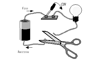
The scissors in Figure 6.1 have cut the circuit, interrupting communications. With the wire cut, regardless of the position of the switch, no current flows through the bulb. To light the bulb, this elementary circuit needs the top switch closed and the bottom wire connected.
Figure 6.1. Whether cut by the switch or the scissors, this circuit is open and no current flows.

It takes two wires to efficiently convey electrical power.
This easy example illustrates an important principle of lumped-element circuit operation ”namely, that current flows only in a complete loop. Another way of expressing the same loop idea is to simply say that if current comes out of the battery, it must return to the battery. That is the way circuits operate in practice. Electrons can't just come out of the battery, pass through the bulb, and then pile up somewhere. The movement of electrons requires a complete loop path .
The current-loop principle may be stated in general mathematical terms:
The total sum of all current going in and out of the battery is zero .
This principle is equivalent to Kirchoff's current law, named after its discoverer, Gustav Robert Kirchoff, 1824 “1887, a German physicist . It applies to all lumped circuit elements (not just batteries), including nonlinear circuits, time-varying circuits, passive circuits, active circuits, and circuits with more than two wires. It remains true even in the presence of distributed parasitic capacitances provided one is careful to include the displacement currents.
Applying this principle to Figure 6.1, cutting the bottom wire prevents current from entering the bottom of the battery; therefore, current is also prevented from leaving at the top.
I hope this discussion makes it clear that you cannot propagate electrical current on just one wire. The propagation of electrical current requires a system of at least two conductors.
Now let's apply this same reasoning to high-speed digital systems. I'll restrict my attention to electrical logic families such as TTL, CMOS, and ECL that have electrical inputs (as opposed to optical or telepathic inputs). First please note that any electric input requires current to operate. Specification sheets may emphasize the performance in terms of voltage specifications, but current is still required. Even on CMOS parts , for which the input current is practically zero, it takes a fair amount of current on every rising edge just to charge the parasitic input capacitance [43] . Every electrical input requires current. As a result, the propagation of every (electrical) logic signal requires a system of at least two conductors. Even though the "second wire" does not appear on a schematic circuit diagram, its presence is required.
[43] It takes 1 mA to charge one picofarad to 1 volt in 1 nanosecond.
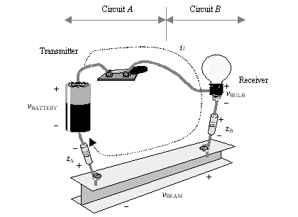
As you probably know, the two-conductor requirement is rather inconvenient. Most digital logic designers would rather use a single wire for each signal, or at least make believe that they are doing so . Toward that end, we designers have adopted a certain convention for the handling of the second wire necessary in all circuits. What we do is hook one side of all transmitters and all receivers to a common reference voltage [44] . In high-speed designs this voltage is usually distributed throughout the system as a ground plane or a pair of power and ground planes. All circuits share this same "second conductor" for the conveyance of returning signal currents. Figure 6.2 illustrates the arrangement for a single transmitter (key switch), receiver (light bulb), and reference system (I-beam). The use of a shared reference voltage for all circuits is called single-ended signaling . Single-ended systems require only one apparent wire for each signal. What one needs to keep in mind about this arrangement is that the second wire is still physically there and that it still physically carries the returning signal currents for each transmitter; it's just implemented as a big, common shared connection.
[44] A global reference voltage may be distributed by means of a solid ground plane, a solid V CC plane, or the Earth itself. Anything can work as long as it ties everything together through a reasonably low impedance.
Figure 6.2. Digital systems use a common ground reference for all returning signal currents. Components z A and z B represent the ground connection impedances of a semiconductor package.

Here's how the circuit in Figure 6.2 works. The transmitter (circuit A ) includes a battery and a switch. One side of the battery connects to a big, solid, shared-reference system (I-beam). This connection between the transmitter circuit and the reference system passes through impedance z A , representing the finite impedance of the package pins or balls used to accomplish this connection.
The receiver (circuit B ) is merely a light bulb connected to the beam through impedance z B . The bulb brightness indicates the condition of the transmitter (switch ON or OFF ). As with the transmitter, the bulb's connection to the common reference beams has a finite impedance.
Provided that the reference-connection impedances are sufficiently low and that there is no significant voltage drop across the steel I-beam, the circuit functions well. When the switch is depressed, the bulb lights.
Let's take a moment to investigate how the finite-impedance reference connections affect the voltage sensed by the bulb. This effect is controlled by the following physical principle:
The battery voltage equals the sum of the voltages across series-connected loads.
This principle is equivalent to Kirchoff's voltage law. It applies to all voltage sources (not just batteries), including nonlinear sources and time-varying sources.
Applied to the circuit in Figure 6.2, Kirchoff's voltage law predicts the following relation:
Equation 6.1

Here I have substituted the expression z A i 1 and z B i 1 for the voltages across the two resistors, with the variable i representing the current flowing around the loop. Presuming that the battery voltage remains constant, if either of the voltages z A i 1 or z B i 1 go up, the voltage across the bulb must go down. Let me state that again in a slightly different way: Anything that affects the voltage drop across z A , z B , or the beam also affects the voltage received at the bulb. This statement uncovers a great weakness of single-ended signaling: The reference voltages at transmitter and receiver must match. Unfortunately, as anyone with an oscilloscope knows , noise exists between every two points on a ground plane (or power plane). If the local reference voltages at the receiver and at the transmitter differ by too great an amount, single-ended signaling can't work.
The difficulty here is that the light bulb has no way of knowing what is the true voltage coming out of the battery. It has no magic connection to the center of the earth with which to measure the true earth potential. It sees only what remains of the transmitted battery voltage after subtraction of the various voltage drops around the signaling loop. In this sense the receiver is a differential receiver . Is responds only to the difference between the voltage on its input terminal and the voltage on its reference terminal (the reference terminal is the ground pin in TTL logic or the most positive power supply pin in ECL logic). All digital receivers operate the same way. Adding 100 mV of noise to the reference pins of a single-ended IC accomplishes precisely the same thing as adding 100 mV of noise directly to every receiver input. This extra noise detracts directly from the available noise margin [45] in your logic family and must be incorporated into any voltage margin analysis for the system.
[45] The noise margin for a logic family is the difference between V OL and V IL , or V OH and V IH , whichever is less.
There is no way around this limitation. If you wish to use single-ended signaling, you must limit the voltage differences within the reference system to a small fraction of the signal amplitude. The impedance of the reference system itself must be low enough to absorb all returning signal currents from all sources without producing objectionable voltage drops at any point.
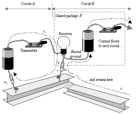
Figure 6.3 depicts another problem inherent to single-ended signaling. This figure incorporates a second transmitter. Assume the second transmitter is part of circuit B . It resides within the same physical package as the receiver; therefore, they share a common ground connection internal to the package. In the figure this shared connection appears as a solid wire connecting the bottom of the light bulb to the bottom of the second battery. This shared internal ground then connects through the impedance of the ground pins or balls on the package (represented by impedance z B ) to the circuit board ground (the I-beam). The boundary of the package containing both the first receiver and the second transmitter is depicted in Figure 6.3 as a box drawn with dashed lines.
Figure 6.3. Ground Bounce: In circuit B , a transmitter and receiver share the same ground connection z B . As current i 2 passes through component z B , it creates voltage “ i 2 z B , which interferes with reception .

Consider what happens when current i 2 flows in the second transmitter circuit. First current i 2 exits the shared package ( dotted region). After circulating through its load, this same current must therefore find its way back inside the shared package. There are only two paths available for current returning to the shared package ”either through impedance z B or through the wire leading to the input port of the receiver (light bulb). In a digital system the impedance z B is much lower (hopefully) than the impedance of the path through the input port, so most of the current reenters the package through z B . So far, so good. Next let's examine the implications of this returning current.
As returning current i 2 reenters the package, it induces voltage “ z B i 2 across the impedance z B . Because impedance z B is shared with the receiving circuit, any voltages appearing across it disturb the apparent voltage received by the light bulb (equation [6.1]). This form of interference goes by the name of common impedance coupling [60] . It happens any time there is any overlap between the paths of current flow for a transmitter and a receiver.
In a high-speed digital application the inductance of the ground connection z B usually causes more difficulties that its resistance. This inductance, multiplied times the di/dt of the returning current, can generate voltages easily sufficient to disturb normal receiver operation. The problem of noise generated by returning signal current acting across the finite impedance of a common ground connection within an IC package is called ground bounce [61] , or more generally simultaneous switching noise [59] .
The same general problem also happens wherever the reference system is weakened or necked-down. Returning signal currents from many drivers, flowing through the finite inductance of the necked-down region, generate differences in the reference potential (with respect to true earth ground) at different points in the system. These voltages can disturb receiver operation. This problem is often called a ground shift , or noisy ground . Noticeable ground shifts often happen across places, like connectors and cables, where the integrity of the solid ground plane has been violated.
Power and ground distributions networks are both susceptible to returning signal currents in the same way. Currents flowing through a power distribution net can perturb the power-supply voltages at various points within the system in the same way that currents in the ground network perturb the ground voltages. Whether you care more about power-supply noise or ground noise depends on whether your single-ended circuits use the power or the ground rail as their internal reference for the discrimination of logic signals. TTL integrated circuits and most high-speed digital CMOS circuits use the ground terminal as the designated reference voltage. ECL circuits powered from ground and “5.2 volts use the ground terminal as the designated reference voltage. ECL circuits powered from a positive supply and ground (sometimes called PECL) use their positive supply terminal as the designated reference voltage.
POINTS TO REMEMBER
- The big advantage of single-ended signaling is that it requires only one wire per signal.
- Single-ended signaling falls prey to disturbances in the reference voltage.
- Single-ended signaling is susceptible to ground bounce.
- Single-ended signaling requires a low-impedance common reference connection.
Fundamentals
- Impedance of Linear, Time-Invariant, Lumped-Element Circuits
- Power Ratios
- Rules of Scaling
- The Concept of Resonance
- Extra for Experts: Maximal Linear System Response to a Digital Input
Transmission Line Parameters
- Transmission Line Parameters
- Telegraphers Equations
- Derivation of Telegraphers Equations
- Ideal Transmission Line
- DC Resistance
- DC Conductance
- Skin Effect
- Skin-Effect Inductance
- Modeling Internal Impedance
- Concentric-Ring Skin-Effect Model
- Proximity Effect
- Surface Roughness
- Dielectric Effects
- Impedance in Series with the Return Path
- Slow-Wave Mode On-Chip
Performance Regions
- Performance Regions
- Signal Propagation Model
- Hierarchy of Regions
- Necessary Mathematics: Input Impedance and Transfer Function
- Lumped-Element Region
- RC Region
- LC Region (Constant-Loss Region)
- Skin-Effect Region
- Dielectric Loss Region
- Waveguide Dispersion Region
- Summary of Breakpoints Between Regions
- Equivalence Principle for Transmission Media
- Scaling Copper Transmission Media
- Scaling Multimode Fiber-Optic Cables
- Linear Equalization: Long Backplane Trace Example
- Adaptive Equalization: Accelerant Networks Transceiver
Frequency-Domain Modeling
- Frequency-Domain Modeling
- Going Nonlinear
- Approximations to the Fourier Transform
- Discrete Time Mapping
- Other Limitations of the FFT
- Normalizing the Output of an FFT Routine
- Useful Fourier Transform-Pairs
- Effect of Inadequate Sampling Rate
- Implementation of Frequency-Domain Simulation
- Embellishments
- Checking the Output of Your FFT Routine
Pcb (printed-circuit board) Traces
- Pcb (printed-circuit board) Traces
- Pcb Signal Propagation
- Limits to Attainable Distance
- Pcb Noise and Interference
- Pcb Connectors
- Modeling Vias
- The Future of On-Chip Interconnections
Differential Signaling
- Differential Signaling
- Single-Ended Circuits
- Two-Wire Circuits
- Differential Signaling
- Differential and Common-Mode Voltages and Currents
- Differential and Common-Mode Velocity
- Common-Mode Balance
- Common-Mode Range
- Differential to Common-Mode Conversion
- Differential Impedance
- Pcb Configurations
- Pcb Applications
- Intercabinet Applications
- LVDS Signaling
Generic Building-Cabling Standards
- Generic Building-Cabling Standards
- Generic Cabling Architecture
- SNR Budgeting
- Glossary of Cabling Terms
- Preferred Cable Combinations
- FAQ: Building-Cabling Practices
- Crossover Wiring
- Plenum-Rated Cables
- Laying Cables in an Uncooled Attic Space
- FAQ: Older Cable Types
100-Ohm Balanced Twisted-Pair Cabling
- 100-Ohm Balanced Twisted-Pair Cabling
- UTP Signal Propagation
- UTP Transmission Example: 10BASE-T
- UTP Noise and Interference
- UTP Connectors
- Issues with Screening
- Category-3 UTP at Elevated Temperature
150-Ohm STP-A Cabling
- 150-Ohm STP-A Cabling
- 150- W STP-A Signal Propagation
- 150- W STP-A Noise and Interference
- 150- W STP-A: Skew
- 150- W STP-A: Radiation and Safety
- 150- W STP-A: Comparison with UTP
- 150- W STP-A Connectors
Coaxial Cabling
- Coaxial Cabling
- Coaxial Signal Propagation
- Coaxial Cable Noise and Interference
- Coaxial Cable Connectors
Fiber-Optic Cabling
- Fiber-Optic Cabling
- Making Glass Fiber
- Finished Core Specifications
- Cabling the Fiber
- Wavelengths of Operation
- Multimode Glass Fiber-Optic Cabling
- Single-Mode Fiber-Optic Cabling
Clock Distribution
- Clock Distribution
- Extra Fries, Please
- Arithmetic of Clock Skew
- Clock Repeaters
- Stripline vs. Microstrip Delay
- Importance of Terminating Clock Lines
- Effect of Clock Receiver Thresholds
- Effect of Split Termination
- Intentional Delay Adjustments
- Driving Multiple Loads with Source Termination
- Daisy-Chain Clock Distribution
- The Jitters
- Power Supply Filtering for Clock Sources, Repeaters, and PLL Circuits
- Intentional Clock Modulation
- Reduced-Voltage Signaling
- Controlling Crosstalk on Clock Lines
- Reducing Emissions
Time-Domain Simulation Tools and Methods
- Ringing in a New Era
- Signal Integrity Simulation Process
- The Underlying Simulation Engine
- IBIS (I/O Buffer Information Specification)
- IBIS: History and Future Direction
- IBIS: Issues with Interpolation
- IBIS: Issues with SSO Noise
- Nature of EMC Work
- Power and Ground Resonance
Points to Remember
Appendix A. Building a Signal Integrity Department
Appendix B. Calculation of Loss Slope
Appendix C. Two-Port Analysis
- Appendix C. Two-Port Analysis
- Simple Cases Involving Transmission Lines
- Fully Configured Transmission Line
- Complicated Configurations
Appendix D. Accuracy of Pi Model
Appendix E. erf( )
Notes
EAN: N/A
Pages: 163
