Intentional Delay Adjustments
Sometimes a small positive (or negative) skew may be desirable. For example, a retarded (or advanced) clock usually improves timing margins for one part of the circuit but worsens them elsewhere. If the "elsewhere" part of the circuit already has a bounteous timing margin, intentionally skewing the clock to fix a local problem makes a lot of sense.
Once you realize that a purposeful, nonzero skew can be useful, you might change your objective for clock design. Instead of seeking to attain everywhere the lowest possible skew, you might view clock design as an exercise in reducing the uncertainty in the clock arrival time. Once the uncertainty is suitably reduced, you can always deal with the necessary fixed adjustments as a second step. Be careful, though. Use purposeful clock skew only when you have a good timing model for the whole circuit.
Adjustments to the clock timing are sometimes called adjustments to the clock phase . This term reminds us that the clock is a repetitive waveform, roughly sinusoidal.
12.8.1 Fixed Delay
The simplest form of clock adjustment is a fixed delay. A fixed delay provides a predetermined amount of clock delay that does not change after assembly. A fixed delay compensates for nominal delays elsewhere in the circuit. Because the delay is frozen at the time of design, a fixed delay cannot cancel variations in trace propagation delay or active component speed, neither of which is known until the circuit is built.
Fixed delays are built from three basic building blocks: transmission lines, chains of logic gates, and discrete circuits. Each has its advantages (Table 12.3). Transmission lines work well for short delays and can be very accurate. Gate delays use less board area than delay lines use but are considerably less accurate. A discrete-circuit delay element covers the widest range of possible delays. Its delay variation depends mainly on the quality of the analog components used in its construction.
Table 12.3. Common Fixed Delay Elements
|
Practical amount of delay realizable (ps) |
Approximate uncertainty in delay (percent) |
|
|---|---|---|
|
Pcb trace (serpentine delay) |
10 “1000 |
±10% |
|
Ordinary logic gate (each) |
100 “10,000 |
±50% or more |
|
Discrete circuit |
1000 “1,000,000 |
±5% to ±20% depending on quality |
|
NOTE ”Gate delays on-chip are considerably less than these numbers . |
||
Delays implemented as transmission lines on pcb require space. For example, at a dielectric constant of 4.3, a 1-ns delay requires a trace length of 0.144 m (5.67 in.). Implemented with a 300- m m trace pitch (11.8 mil), each nanosecond of delay consumes approximately 0.43 square cm of board real estate (0.067 sq. in.).
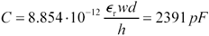
When using a pc trace as a transmission line-delay, keep in mind the variation in relative permittivity of the trace with temperature. For FR-4 material, this variation results in a considerable change in propagation velocity over the temperature range of 0 to 70 °C. The variation is most easily measured for your material using a bare board with copper foil on both sides. Attach a handheld capacitance meter with long leads to the board to record the capacitance between the foil plates. If the board is .3 x .3m, with a core thickness of 1.5 mm (60 mils) and a dielectric constant of 4.5 at 1 MHz, the expected value of capacitance is
Equation 12.5
|
where |
the dielectric constant |
|
the board width w is 0.3 m (12 in.), |
|
|
the board depth d is 0.3 m (12 in.), and |
|
|
the board thickness h is 1.5 x 10 “3 m (60 mil). |
 r at 1 MHz,
Try the experiment with the leads alone and then with the leads touching the board so you can calibrate out the capacitance of the leads. Now place the board (but not the meter) in a temperature-controlled oven and measure the percentage change in capacitance over your range of temperatures . The percentage change in trace velocity, being related to the square root of the dielectric constant, will vary by half the percentage change in the dielectric constant.
Some commercial delay lines are built from a transmission line surrounded by a magnetically permeable material. The permeable material radically increases the delay per inch, shrinking the physical size of the delay line. These delay lines are available with or without buffering.
A spare gate makes an effective delay element. Such an approach is often used to guarantee compliance with a register hold time. The problem with using a gate for a delay element is that while all manufacturers specify maximum propagation delay, few talk about the minimum gate delay. The total variation in gate delay is so large that sometimes the use of a gate as a delay element hinders rather than helps clock skew. Unfortunately, inside a gate array or custom chip, there may be no choice but to use a gate for a delay element.
The discrete-circuit delay in Figure 12.24 produces clean, repeatable delays when used with CMOS gates. The slow risetime of the RC circuit retards the propagation of pulses from the first gate to the second gate by an amount approximately equal to the RC time constant.
Figure 12.24. This circuit easily produces delays many times larger than an individual gate delay.
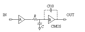
If this circuit is built from bipolar gates (or any gates that require substantial amounts of DC input current), the signal at the input to the second stage may fail to rise or fall to a level sufficient to cause reliable switching if R is too large. This happens because of the voltage drop I IH R (or “I IL R ) across the resistor. An inductive bead or a wound inductor used as the series loss element has no loss at DC and so would pass the required input current without introducing a voltage drop. CMOS logic doesn't require any DC input current, and so just about any value of resistor R works (even 1 M W ).
The accuracy of the delay circuit in Figure 12.24 depends mostly on the tolerance of components R and C , the parasitic input capacitance of the second gate, the switching threshold of the second stage, and the variability in delay of gates A and B. A differential receiver with a tightly controlled threshold (i.e., low offset voltage) would diminish the variability of this circuit. As you stretch the delay to amounts greatly in excess of the natural delay of gate B, the input at B becomes highly susceptible to noise due to the slow transition speed at that point. A Schmidt trigger at B will prevent oscillation near the threshold point, but will not improve the noise characteristics. A simple Schmidt-trigger feature ( C /10) appears with dotted lines in Figure 12.24. If you need accurate, long-term delays, the circuit must be protected from crosstalk and provided with its own privately filtered power source.
Whatever form of fixed delay you choose, incorporate its delay uncertainty into your timing-margin calculations.
12.8.2 Adjustable Delays
An adjustable delay can compensate for actual as well as for nominal delays in a circuit. The adjustment, if properly set, reduces the uncertainty in clock skew caused by variations in board fabrication and active component delay. Unfortunately, the weakness in this approach is that technicians must make adjustments after assembly as part of the final test process.
Do not assume your manufacturing staff will understand the meaning of the adjustments provided. Write a test procedure for each adjustment, showing how to measure the clock delay at that point and indicating the limits of proper adjustment.
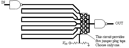
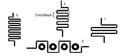
A delay line may be adjusted in quantized steps. The layout in Figure 12.25 illustrates a typical end- terminated adjustable delay. The transmission line has five adjustment taps. Provided that the five-way collection circuit on the right side of the diagram is short compared to the length of a rising (or falling) edge, the circuit works beautifully.
Figure 12.25. An adjustable delay line can be set to any of a number of fixed delay taps.
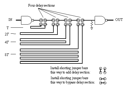
A more flexible arrangement appears in Figure 12.26, which produces 16 different delays with only 8 jumpers . The jumper sizes in Figure 12.26 are tuned to one, two, four, and eight times a basic delay T. The switches can select any combination of delay sections. Although the circuit in Figure 12.26 is technically more powerful, its complexity works against you, because complexity breeds mistakes.
Figure 12.26. This adjustable delay provides 16 settings with only 8 jumpers.
A s horting plug makes a good adjustable tap at low frequencies. These tiny, removable plugs fit onto a pair of 0.025-in.-square posts separated by 0.100-in. (Figure 12.27). Some people call shorting plugs software jumper s because of their prevalence as option jumpers on personal computer add-on cards. Above 100 MHz you may notice some side effects from the inductance of a shorting plug. [117] The inductance varies according to how far down the posts you have pressed the plug. For laboratory purposes, I've seen this effect used as a way to implement a simple adjustable delay (but it's not robust enough for use in field applications).
[117] A plug with 0.1-in. pins on a 0.1-in. spacing produces an inductance somewhere in the range of 1 to 3 nH, depending on the shape of the conductors within the plug housing.
Figure 12.27. The solder blob jumper, being smaller, has better high-frequency properties than a shorting plug.
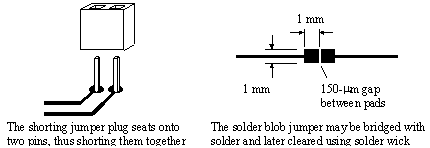
If the inductance of the jumper plugs is not acceptable, try solder blob jumpers (Figure 12.27). A solder blob jumper consists of two 0.50-in.-square pads separated by a 0.006-in. space. The 0.006-in. gap is wide enough to prevent solder bridging during assembly, yet narrow enough to be easily bridged by a technician or by a blob of solder paste deposited during manufacturing. A bridged solder blob clears quickly and cleanly with solder wick. Compared to shorting jumper bars, solder blob switches take very little circuit board area. Another advantage of solder blob jumpers is that they don't fall off or move after assembly.
Gate delays may also be adjusted in quantized steps. A chain of gates tapped at discrete points makes a usable delay line. Delay circuits built from gates suffer from the basic inaccuracy of each gate delay. Otherwise, they behave much like a tapped transmission line.
A discrete-circuit delay may be adjusted by varying either R or C. Continuously variable resistors are cheaper and easier to get than variable capacitors. With either type, provide some mechanism for clamping or gluing the adjustment after setting it. Adjustable components are particularly susceptible to vibration .
Some step-variable passive components are available that incorporate several component values plus a tiny set of solder blob jumpers all on a 1206 surface-mount body. Such parts would allow quantized tuning of R-C delay circuits.
12.8.3 Automatically Programmable Delays
An ideal delay circuit would be continuously variable, would be stable over a wide temperature range, and would adjust itself in production. Sound impossible ? Read on.
First let's see how to make a continuously programmable delay. Two approaches show promise in this arena. The oldest involves a varactor diode. The varactor diode is a diode whose parasitic capacitance varies as a function of applied reverse bias. Normally a hindrance to design, parasitic capacitance in the varactor is its primary selling point. The difficulty with using varactor diodes is that to obtain a wide range of capacitance, the device must be biased at a reverse-bias voltage significantly higher than the forward voltage drop across the diode. This typically requires at least a 12-volt (preferably 24-volt) power supply.
A second programmable delay approach uses a chain of gates. If all the gates are internal to one integrated circuit, the chain can be very long. A tapped version of the gate chain, with a giant multiplexer to select between taps, forms a useful digitally programmable delay. The design of the multiplexer must prevent glitches, which might occur when switching from one tap to the next .
Several manufacturers now produce clock repeater chips that can be programmed to intentionally skew their outputs. This trend will likely continue, with even more flexibility and granularity introduced in each successive generation of clock repeaters. [118]
[118] For example, see the Cypress CY7B991V "Roboclock" and the IDT IDT5T9950/A "Turboclock Jr."
Modulating the power-supply voltage to the entire chain is an interesting and effective way to change the total delay. This works because CMOS gates switch much more slowly when starved for power. The power- starvation effect, normally viewed as a troublesome source of undesirable variation, can be used to create continuously adjustable chains of delay.
With any adjustable delay circuit, you can store a table listing proper adjustment settings as a function of temperature. That improves the circuit's temperature stability. Better yet, set up a second dummy delay and tune its performance using a DLL until it matches an external standard (such as one clock period from a crystal oscillator). Then adjust your main delay using the same parameters. This technique gives you some hope of compensating for temperature, aging, and process variations.
If you want your chain of N delays to add up to precisely one clock period (making a multiphase clock generator), just run the output of the last delay along with the clock into a phase detector. Use the phase detector output to adjust the whole chain until you achieve a total delay of precisely one clock period. Presuming the delays of each stage are equal, the outputs so generated will precisely divide the clock into equal- sized intervals. For this purpose a chain of invertors works better than a chain of buffers. The invertors tend to better maintain a 50% duty cycle as you go down the chain.
Finally, consider how a clock-phase adjustment circuit used on a bus might automatically tune itself. As your clock skews out of adjustment in either direction, your system will likely show a marked increase in its error rate. You can detect that increase and then center the clock between the error-prone zones.
Alternately, you could directly sense the switching times of data signals on your bus. The receiving clock could then be automatically adjusted to match the transition times in the data waveform. This method is directly analogous to the clock recovery architectures used in serial data transmission.
POINTS TO REMEMBER
- Delay elements are built from three basic building blocks: transmission lines, logic gates, and passive lumped circuits.
- A fixed delay cannot cancel variations in board fabrication or active component delay.
- An adjustable delay compensates for actual delays, not just nominal delays, elsewhere in the circuit.
- Whatever form of delay you choose, incorporate its uncertainty in delay into your timing margin calculations.
12.8.4 Serpentine Delays
12.8.5 Switchback Coupling
Figure 12.29 illustrates three microstrip delay-line layouts with identical total trace length, but substantially different performance.
Figure 12.29. These three delay-line layouts have the same overall length but different delays.
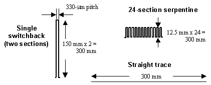
The first layout is a single switchback, also known as a two-section serpentine. The two elements used in this design are each 150 mm long, for a total of 300 mm. The traces are laid out using a 200-130-200 m m pattern (8-5-8 mils), meaning that a plan view of the board would show one 200- m m trace, one 130- m m space, and another 200- m m trace. The trace pitch (distance between trace centerlines) is 330 m m. The trace height is 130 m m, yielding a trace impedance of approximately 50 W .
The second layout is a more convoluted serpentine built from 24 sections of 0.5 inches each, again using the 200-130-200 m m trace-width pattern.
The third layout is a straight 50- W trace.
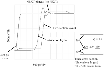
Figures 12.30 and 12.31 illustrate the nature of serpentine coupling on all three layouts. [119] In the simulations all trace losses have been neutralized and perfect terminations used, so the only artifacts present are the NEXT and FEXT coupling between adjacent sections of the switchbacks.
[119] Computed using HyperLynx LineSim v.5.01.
Figure 12.30. Viewed at the receiver, NEXT from a single switchback (U-turn) generates plateaus both before and after the main edge.
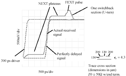
Figure 12.31. Viewed at the receiver, when the section length is much shorter than the signal risetime, the NEXT effects blend together, creating the appearance of an accelerated received edge.
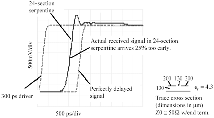
Figure 12.30 compares the two-section layout with the straight trace. The first curve (leftmost) is the output of the simulated 3.3-V CMOS driver with 300-ps risetime. The second curve represents the output of the two-section serpentine (single switchback). The third curve is the output of a perfectly straight trace 300 mm long. The straight trace yields a simple delay of 1680 ps, but that's not what happens on the switchback.
In the second curve you can clearly see the effects of serpentine coupling. NEXT coupling between the adjacent members of the switchback superimposes a 300-mV precursor and a 300-mV postcursor onto the received edge. The precursor and postcursor are each 1680 ps long, corresponding to one switchback delay. In addition to the NEXT coupling, there is another pulse following the main edge by 1680 ps. This other pulse has a duration approximately equal to the signal risetime and an amplitude of 500 mV. This is the effect of FEXT coupling, which in a switchback appears substantially after the arrival of the main edge. [120] The NEXT and FEXT distortions, if compounded over several switchback sections, render the structure useless.
[120] Viewed at the receiver, the delay between the arrival of the main edge and the arrival of the FEXT pulse equals the propagation delay of the switchback.
The NEXT precursor is generated as the main signal passes up the left-hand side of the switchback, creating positive NEXT on the right-hand side moving in the downward direction, towards the receiver in advance of the main edge. The NEXT postcursor is generated when the main signal passes over the top of the switchback and begins its descent down the right-hand leg, creating positive NEXT on the leftmost leg moving in the upwards direction, towards the receiver, but lagging the main edge.
The FEXT waveform is generated in a direction always moving opposite to the main edge. In a microstrip the polarity will be negative polarity (striplines have little or no FEXT). I assume in Figure 12.30 that the FEXT pulse bounces off the relatively low-impedance of the driver, inverting its polarity. As the main edge exits the bottom right-hand corner of the switchback, the last increment of FEXT is generated at the bottom left-hand corner of the switchback. This bit of FEXT bounces off the driver and arrives one full propagation delay after the arrival of the main edge.
The reason you are able to discern the NEXT and FEXT coupling as separate events in Figure 12.30 is because in this case the switchback delay (1680 ps) is substantially larger than the signal risetime. If you were to reverse that situation, constructing the whole serpentine structure instead from a larger number of smaller switchback sections, the distortion in the main signal would become far less of a problem.
Figure 12.31 makes such a change. It shows the effect of a 24-section serpentine on a signal with a risetime of 300 ps. In this figure the NEXT and FEXT coupling ratios between successive traces within the serpentine structure are the same as in Figure 12.30; however, in this case the precursor and postcursor lengths, being related to the length of each individual switchback section, have been reduced by a factor of 12. The pattern of crosstalk superposition in this case does not produce significant waveform distortion; instead it merely advances the time of arrival of each rising (or falling) edge. Apparently, it's okay to have coupling between sections provided that each section is much shorter (in delay) than the signal rise (or fall) time, and further provided that you remember that the overall delay will be shorter than the total trace length might indicate.
For coupled serpentines, when the switchback sections are a small fraction (maybe 1/3 or less) of the rise (or fall) time, the reduction is delay due to NEXT coupling can theoretically be as much as 4 times the NEXT coefficient. In the 24-section serpentine example shown here, a NEXT coefficient of only about 10% reduced the overall delay by about 25%.
Stripline serpentines show precisely the same NEXT effect, but without the FEXT (Figure 12.32). The output waveform from a multisection stripline serpentine may therefore look somewhat cleaner than the waveform from a microstrip serpentine. The trace dimensions in this example have been adjusted to create a trace pitch and impedance similar to the microstrip examples in Figures 12.30 and 12.31. Because of the stripline configuration the NEXT coefficient, and consequently the degree of loss in delay, is somewhat less.
Figure 12.32. A tightly coupled stripline serpentine, just like the microstrip, suffers a reduction in delay.
If you want to implement your serpentine in the minimum amount of physical space, you should use short sections, squeeze the traces together, and in the final implementation add sections to compensate for the loss in delay due to coupling. If, on the other hand, you want your delay to come out perfect on the first spin, then you should spread the traces out sufficiently far to eliminate concern about switchback coupling.
POINT TO REMEMBER
- Avoid long, coupled switchbacks.
Fundamentals
- Impedance of Linear, Time-Invariant, Lumped-Element Circuits
- Power Ratios
- Rules of Scaling
- The Concept of Resonance
- Extra for Experts: Maximal Linear System Response to a Digital Input
Transmission Line Parameters
- Transmission Line Parameters
- Telegraphers Equations
- Derivation of Telegraphers Equations
- Ideal Transmission Line
- DC Resistance
- DC Conductance
- Skin Effect
- Skin-Effect Inductance
- Modeling Internal Impedance
- Concentric-Ring Skin-Effect Model
- Proximity Effect
- Surface Roughness
- Dielectric Effects
- Impedance in Series with the Return Path
- Slow-Wave Mode On-Chip
Performance Regions
- Performance Regions
- Signal Propagation Model
- Hierarchy of Regions
- Necessary Mathematics: Input Impedance and Transfer Function
- Lumped-Element Region
- RC Region
- LC Region (Constant-Loss Region)
- Skin-Effect Region
- Dielectric Loss Region
- Waveguide Dispersion Region
- Summary of Breakpoints Between Regions
- Equivalence Principle for Transmission Media
- Scaling Copper Transmission Media
- Scaling Multimode Fiber-Optic Cables
- Linear Equalization: Long Backplane Trace Example
- Adaptive Equalization: Accelerant Networks Transceiver
Frequency-Domain Modeling
- Frequency-Domain Modeling
- Going Nonlinear
- Approximations to the Fourier Transform
- Discrete Time Mapping
- Other Limitations of the FFT
- Normalizing the Output of an FFT Routine
- Useful Fourier Transform-Pairs
- Effect of Inadequate Sampling Rate
- Implementation of Frequency-Domain Simulation
- Embellishments
- Checking the Output of Your FFT Routine
Pcb (printed-circuit board) Traces
- Pcb (printed-circuit board) Traces
- Pcb Signal Propagation
- Limits to Attainable Distance
- Pcb Noise and Interference
- Pcb Connectors
- Modeling Vias
- The Future of On-Chip Interconnections
Differential Signaling
- Differential Signaling
- Single-Ended Circuits
- Two-Wire Circuits
- Differential Signaling
- Differential and Common-Mode Voltages and Currents
- Differential and Common-Mode Velocity
- Common-Mode Balance
- Common-Mode Range
- Differential to Common-Mode Conversion
- Differential Impedance
- Pcb Configurations
- Pcb Applications
- Intercabinet Applications
- LVDS Signaling
Generic Building-Cabling Standards
- Generic Building-Cabling Standards
- Generic Cabling Architecture
- SNR Budgeting
- Glossary of Cabling Terms
- Preferred Cable Combinations
- FAQ: Building-Cabling Practices
- Crossover Wiring
- Plenum-Rated Cables
- Laying Cables in an Uncooled Attic Space
- FAQ: Older Cable Types
100-Ohm Balanced Twisted-Pair Cabling
- 100-Ohm Balanced Twisted-Pair Cabling
- UTP Signal Propagation
- UTP Transmission Example: 10BASE-T
- UTP Noise and Interference
- UTP Connectors
- Issues with Screening
- Category-3 UTP at Elevated Temperature
150-Ohm STP-A Cabling
- 150-Ohm STP-A Cabling
- 150- W STP-A Signal Propagation
- 150- W STP-A Noise and Interference
- 150- W STP-A: Skew
- 150- W STP-A: Radiation and Safety
- 150- W STP-A: Comparison with UTP
- 150- W STP-A Connectors
Coaxial Cabling
- Coaxial Cabling
- Coaxial Signal Propagation
- Coaxial Cable Noise and Interference
- Coaxial Cable Connectors
Fiber-Optic Cabling
- Fiber-Optic Cabling
- Making Glass Fiber
- Finished Core Specifications
- Cabling the Fiber
- Wavelengths of Operation
- Multimode Glass Fiber-Optic Cabling
- Single-Mode Fiber-Optic Cabling
Clock Distribution
- Clock Distribution
- Extra Fries, Please
- Arithmetic of Clock Skew
- Clock Repeaters
- Stripline vs. Microstrip Delay
- Importance of Terminating Clock Lines
- Effect of Clock Receiver Thresholds
- Effect of Split Termination
- Intentional Delay Adjustments
- Driving Multiple Loads with Source Termination
- Daisy-Chain Clock Distribution
- The Jitters
- Power Supply Filtering for Clock Sources, Repeaters, and PLL Circuits
- Intentional Clock Modulation
- Reduced-Voltage Signaling
- Controlling Crosstalk on Clock Lines
- Reducing Emissions
Time-Domain Simulation Tools and Methods
- Ringing in a New Era
- Signal Integrity Simulation Process
- The Underlying Simulation Engine
- IBIS (I/O Buffer Information Specification)
- IBIS: History and Future Direction
- IBIS: Issues with Interpolation
- IBIS: Issues with SSO Noise
- Nature of EMC Work
- Power and Ground Resonance
Points to Remember
Appendix A. Building a Signal Integrity Department
Appendix B. Calculation of Loss Slope
Appendix C. Two-Port Analysis
- Appendix C. Two-Port Analysis
- Simple Cases Involving Transmission Lines
- Fully Configured Transmission Line
- Complicated Configurations
Appendix D. Accuracy of Pi Model
Appendix E. erf( )
Notes
EAN: N/A
Pages: 163
