IBIS: Issues with Interpolation
IBIS Issues with Interpolation
An IBIS model specifies two I-V tables for each driver, one representing the static behavior of the driver when switched to the low state and another I-V curve representing the driver in the high state. In addition, the file provides other information that says how to morph from one I-V table to the other (see Figure 13.5). The purpose of morphing is to produce, at each point in time, a complete I-V table that a SPICE-like simulation engine can use to compute circuit results.
Figure 13.5. IBIS specifies a rate at which the low-state I-V curve morphs into the high-state I-V curve.
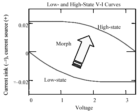
The form of the morphing information you will see inside an IBIS file depends on which version of the IBIS format you are using. The oldest (and simplest) IBIS specification included nothing more than a transition rate. The transition rate provides some gross information about how to morph from the low table to the high table, but as with any interpolation process, the exact form of interpolation used affects the accuracy of the final result. For example, software vendors that implement the transition as a strictly linear ramp create waveforms significantly different from those that use quadratic smoothing at the corners of each rising or falling edge.
More recent IBIS specifications include rising and falling waveform specifications. These specifications include samples of the (rising or falling) waveform as observed under particular measurement conditions. The measurement conditions used are called out as part of each waveform specification. There may be more than one waveform specification.
For CMOS totem-pole drivers, a good IBIS model provides two rising edge waveforms ”one measured with a 50- W load to ground and one measured with a 50- W load to V CC . The model also provides two falling waveforms, for a total of four combinations of behavior showing rising and falling waveforms under both load conditions.
I rate such a model as good because I believe that such measurement conditions span the range of circumstances under which critical evaluation of signal shape is most important for CMOS drivers. For emitter-follower type drivers (ECL, PECL, and some GaAs), one waveform of each type measured with a 50- W load to the appropriate termination voltage will suffice. For pull-down only drivers like RAMBUS, GTL, and BTL one waveform of each type measured with a 25- W load (or whatever is appropriate in your system) to the appropriate termination voltage will suffice.
If only one waveform of each type is to be measured for a CMOS driver it should be measured using a symmetrically split end-termination.
An IBIS simulator uses the measured waveforms to improve the accuracy of its calculations. To understand how, you need a little information about the IBIS chip model.
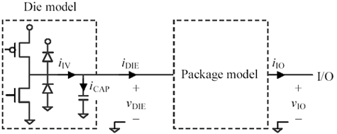
Your IBIS simulator assumes each chip incorporates a totem-pole driver, some protection diodes, and a lumped-element capacitance representing the aggregate capacitance of the FETs and diodes (Figure 13.6). The totem-pole stage and the protection diodes are assumed to be memory-less, meaning that their actions can be completely described by an I-V curve. The curve may vary with time, but at any instant it has a particular shape. The capacitance is assumed to be both linear and time-invariant .
Figure 13.6. The IBIS die model includes a capacitor whose action must be de-embedded from the I-V table.

Your IBIS simulator is faced with the task of discovering a time-varying I-V function that satisfies four constraints:
- In the steady-state high condition it mimics the high I-V table provided in the IBIS specification.
- In the steady-state low condition it mimics the low I-V table provided in the IBIS specification.
- During a rising edge, with the load called out in the specification, it mimics the rising waveform samples provided in the IBIS specification.
- During a falling edge, with the load called out in the specification, it mimics the falling waveform samples provided in the IBIS specification.
One possible way to solve this problem is to concoct a hypothetical I-V function that is a linear combination of the low and high I-V tables provided. [134]
[134] Not all simulator vendors use this method.
Equation 13.1

|
where |
i TP ( v , t ) represents the time-varying I-V function associated with the totem-pole and diode components in Figure 13.6, |
|
i LOW represents the low I-V table provided in the IBIS specification, |
|
|
i HIGH represents the high I-V table provided in the IBIS specification, and |
|
|
a ( t ) and b ( t ) are scalar functions of time. |
The functions a ( t ) and b ( t ) are discovered by first de-embedding the die capacitance from the measurements and then solving for the functions a ( t ) and b ( t ) that satisfy constraints numbered 3 and 4. The complete die model is composed of the time-varying I-V relationship [13.1] placed in parallel with the shunt die capacitance. This method was described by Bernhard Unger and Manfred Maurer of Siemens AG at the February 1998 IBIS summit meeting, SI-Analysis with HSPICE based on IBIS Models (see IBIS archives at [104] ).
The de-embedding of the capacitance has a direct bearing on the accuracy of the results, because the rising and falling waveforms are defined at the die, including the capacitor ( v DIE in Figure 13.6), but the I-V curves you seek are defined at the output of the totem-pole and diode stage prior to the capacitor.
Using the rising waveform specified as part of the IBIS model, and given knowledge of the load conditions, your IBIS simulator can compute the current i DIE flowing out of the die and into the load at every point in time during one rising edge. Your simulator can also compute the current flowing through the capacitor, i CAP , assuming it knows accurately the dv / dt of the measured waveform and the value of the die capacitance. The simulator then adds i DIE and i CAP to find the current i TP coming out of the totem-pole stage. This calculation is called the de-embedding process . After de-embedding the die capacitance the simulator knows, for each point in time during the rising edge, a pair of current and voltage values ( i TP and v DIE ) which together represent one point on the I-V table for the totem-pole stage at that particular time with that particular load.
If only one rising waveform is available the simulator uses the de-embedded information to solve for a ( t ) and b ( t ) under the additional assumption that the two functions sum to unity.
If a second rising waveform is available measured under different conditions of loading, then your simulator can deduce two points on the totem-pole I-V curve for every moment in time, which is just enough information to solve independently for the coefficients a ( t ) and b ( t ). This dual-waveform solution produces a rising edge model better suited for extrapolation to other conditions of loading.
The procedure is repeated to compute values of a ( t ) and b ( t ) for falling edges.
If the assumed die capacitance doesn't match the actual die capacitance present during laboratory measurement (or SPICE simulation), then the coefficients a ( t ) and b ( t ) will not come out quite right. The result of that inaccuracy is that waveforms predicted under conditions similar to the measurement conditions will come out just fine, but as you move away from the measurement conditions to other types of loads, the predicted waveforms become increasingly erroneous. This effect highlights a very important concept relevant to all interpolation algorithms:
Always specify circuit behavior under conditions similar to the actual conditions present in your application.
For example, high-speed drivers rarely encounter 50-pF lumped capacitances in real-world applications; therefore, the old 50-pF timing specification makes little or no sense. For high-speed parts , it is much better to specify the performance of your driver into a 50- W load and then extrapolate from there to determine what would happen with the occasional 50-pF load.
If your waveform measurements are taken on a packaged component (at point v IO in Figure 13.7), then the entire package model must first be de-embedded to determine the die waveforms. This operation is generally beyond the scope of an IBIS simulator, although it is certainly within the realm of reason that someone would take packaged-chip measurements and from that attempt to intuit the die waveforms.
Figure 13.7. IBIS models a chip die and its associated package separately.
POINT TO REMEMBER
- Specify circuit behavior under conditions similar to the actual conditions present in your application.
Fundamentals
- Impedance of Linear, Time-Invariant, Lumped-Element Circuits
- Power Ratios
- Rules of Scaling
- The Concept of Resonance
- Extra for Experts: Maximal Linear System Response to a Digital Input
Transmission Line Parameters
- Transmission Line Parameters
- Telegraphers Equations
- Derivation of Telegraphers Equations
- Ideal Transmission Line
- DC Resistance
- DC Conductance
- Skin Effect
- Skin-Effect Inductance
- Modeling Internal Impedance
- Concentric-Ring Skin-Effect Model
- Proximity Effect
- Surface Roughness
- Dielectric Effects
- Impedance in Series with the Return Path
- Slow-Wave Mode On-Chip
Performance Regions
- Performance Regions
- Signal Propagation Model
- Hierarchy of Regions
- Necessary Mathematics: Input Impedance and Transfer Function
- Lumped-Element Region
- RC Region
- LC Region (Constant-Loss Region)
- Skin-Effect Region
- Dielectric Loss Region
- Waveguide Dispersion Region
- Summary of Breakpoints Between Regions
- Equivalence Principle for Transmission Media
- Scaling Copper Transmission Media
- Scaling Multimode Fiber-Optic Cables
- Linear Equalization: Long Backplane Trace Example
- Adaptive Equalization: Accelerant Networks Transceiver
Frequency-Domain Modeling
- Frequency-Domain Modeling
- Going Nonlinear
- Approximations to the Fourier Transform
- Discrete Time Mapping
- Other Limitations of the FFT
- Normalizing the Output of an FFT Routine
- Useful Fourier Transform-Pairs
- Effect of Inadequate Sampling Rate
- Implementation of Frequency-Domain Simulation
- Embellishments
- Checking the Output of Your FFT Routine
Pcb (printed-circuit board) Traces
- Pcb (printed-circuit board) Traces
- Pcb Signal Propagation
- Limits to Attainable Distance
- Pcb Noise and Interference
- Pcb Connectors
- Modeling Vias
- The Future of On-Chip Interconnections
Differential Signaling
- Differential Signaling
- Single-Ended Circuits
- Two-Wire Circuits
- Differential Signaling
- Differential and Common-Mode Voltages and Currents
- Differential and Common-Mode Velocity
- Common-Mode Balance
- Common-Mode Range
- Differential to Common-Mode Conversion
- Differential Impedance
- Pcb Configurations
- Pcb Applications
- Intercabinet Applications
- LVDS Signaling
Generic Building-Cabling Standards
- Generic Building-Cabling Standards
- Generic Cabling Architecture
- SNR Budgeting
- Glossary of Cabling Terms
- Preferred Cable Combinations
- FAQ: Building-Cabling Practices
- Crossover Wiring
- Plenum-Rated Cables
- Laying Cables in an Uncooled Attic Space
- FAQ: Older Cable Types
100-Ohm Balanced Twisted-Pair Cabling
- 100-Ohm Balanced Twisted-Pair Cabling
- UTP Signal Propagation
- UTP Transmission Example: 10BASE-T
- UTP Noise and Interference
- UTP Connectors
- Issues with Screening
- Category-3 UTP at Elevated Temperature
150-Ohm STP-A Cabling
- 150-Ohm STP-A Cabling
- 150- W STP-A Signal Propagation
- 150- W STP-A Noise and Interference
- 150- W STP-A: Skew
- 150- W STP-A: Radiation and Safety
- 150- W STP-A: Comparison with UTP
- 150- W STP-A Connectors
Coaxial Cabling
- Coaxial Cabling
- Coaxial Signal Propagation
- Coaxial Cable Noise and Interference
- Coaxial Cable Connectors
Fiber-Optic Cabling
- Fiber-Optic Cabling
- Making Glass Fiber
- Finished Core Specifications
- Cabling the Fiber
- Wavelengths of Operation
- Multimode Glass Fiber-Optic Cabling
- Single-Mode Fiber-Optic Cabling
Clock Distribution
- Clock Distribution
- Extra Fries, Please
- Arithmetic of Clock Skew
- Clock Repeaters
- Stripline vs. Microstrip Delay
- Importance of Terminating Clock Lines
- Effect of Clock Receiver Thresholds
- Effect of Split Termination
- Intentional Delay Adjustments
- Driving Multiple Loads with Source Termination
- Daisy-Chain Clock Distribution
- The Jitters
- Power Supply Filtering for Clock Sources, Repeaters, and PLL Circuits
- Intentional Clock Modulation
- Reduced-Voltage Signaling
- Controlling Crosstalk on Clock Lines
- Reducing Emissions
Time-Domain Simulation Tools and Methods
- Ringing in a New Era
- Signal Integrity Simulation Process
- The Underlying Simulation Engine
- IBIS (I/O Buffer Information Specification)
- IBIS: History and Future Direction
- IBIS: Issues with Interpolation
- IBIS: Issues with SSO Noise
- Nature of EMC Work
- Power and Ground Resonance
Points to Remember
Appendix A. Building a Signal Integrity Department
Appendix B. Calculation of Loss Slope
Appendix C. Two-Port Analysis
- Appendix C. Two-Port Analysis
- Simple Cases Involving Transmission Lines
- Fully Configured Transmission Line
- Complicated Configurations
Appendix D. Accuracy of Pi Model
Appendix E. erf( )
Notes
EAN: N/A
Pages: 163
