Modeling Vias
I have observed a great variety of models proposed for the analysis of vias. Everything has been tried from a zero-order model (ignore it) to a complicated S-parameter characterization painstakingly crafted from three-dimensional field simulations. Applying a via model is only half the battle, deciding how elaborate a model to use is equally important.
For general-purpose digital work using binary signaling you will need only three echelons of modeling.
|
None |
Ignores the via, assuming it has no significant effect. |
|
First order |
The via acts as a single lumped-element reactance, either a shunt capacitance or a series inductance. |
|
Pi model |
The via exhibits the characteristics of both capacitance and inductance, including the possibility of resonance . |
Before discussing these three models in detail, we must define the incremental capacitance and inductance of a via.
5.5.1 Incremental Parameters of a Via
The low-frequency (static) mutual capacitance between a via and its surrounding reference planes may be easily measured or simulated with the via standing in isolation, having no traces attached. When making this measurement the reference planes should be tied to each other, but not to the via under test.
Although such a measurement is well defined, there arise several difficulties with the test setup, as illustrated in the following thought experiment.
Suppose you measure the capacitance of a certain length of pcb trace. Then separately you measure the capacitance of a via, in isolation from the trace. If you now move the trace (by re-laying out the board) to connect it to the via, the total capacitance of the combination is less than the sum of the individual capacitances of the trace and via. The capacitances add in a non-linear way. This illustrates a general rule of capacitive combinations.
The capacitance to ground of any compound structure is always less than the sum of the capacitances to ground of its parts .
This rule applies to any bits of metal near a common reference plane, or sandwiched between two reference planes. It applies whether the planes carry ground or power. In the context of our via discussion, the rule says it is not enough to separately measure the capacitance of a trace and a via and then add them together. The properties of a via are modified by the trace to which it is attached.
The second difficulty with defining the properties of a via in isolation from its trace is that such measurements cannot be used to infer inductance. The inductance of a via depends critically upon the shape of the via and also the path of returning signal current .
In the evaluation of via capacitance you would never think of calculating the capacitance of a via floating in space, totally isolated from the planes. Obviously, it is the interaction between the via and the planes that matters. To talk about the partial capacitance of a via doesn't make much sense.
For similar reasons, this author dislikes very much the concept of "partial inductance." That concept has misled generations of engineers into believing that a via (or a wire) has, by itself, a well-defined value of inductance. It doesn't. Inductance becomes measurable if and only if you specify how and where current returns from the far end of the via (or the wire) back to the source.
To be fair, the partial inductance method does stipulate that you must take into account the partial inductance of the via, the partial inductance of the return path, and the mutual inductance between the two paths. Properly computed, the partial inductance method will reveal the correct answer, but only when you follow the method to completion. Along the way many engineers drop out of the process, omitting the crucial mutual-inductance correction terms and leaving themselves convinced that a via (or wire) by itself has a well-defined inductance.
I would have you remember that inductance is a property only of an entire current pathway (a loop of current). Changing the shape of the return path affects inductance just as much as changing the signal path.
It makes no sense to define, or to attempt to measure, the inductance of a via without also specifying how the attached traces bring current through it, and how the planes carry the returning signal current.
The foregoing difficulties with the definition of an isolated via have convinced me that via measurements should always be undertaken with the traces connected, and with the planes performing their job of carrying the returning signal currents in a realistic way.
To properly measure the incremental shunt capacitance of a via, C V , first measure the static capacitance to the reference planes of a configuration that includes an input trace of length x , the via, and an output trace of length y , where both x and y greatly exceed the clearance-hole diameter. The lengths x and y are measured to the center of the drilled via hole. Then separately measure the static capacitance of a similar trace of length x + y (with no via and no clearance hole). The incremental capacitance contributed by the via is defined as the difference between your two measurements (see Figure 5.28).
Figure 5.28. The measurement process cancels the effect of fringing-field capacitances due to the cut ends of the trace at A and B with equal fringing-field capacitances at C and D.
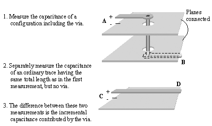
The purpose of extending the traces well beyond the clearance hole is to separate the fields near the via, which you are trying to measure, from the fields near the ends of the traces, which cancel when you take the difference between the two measurements. The planes must be electrically connected during this measurement.
The incremental series inductance of a via, L V , is defined similarly, but with each trace shorted to the reference plane at its far end. Arrange your equipment to detect the loop inductance of the path entering the trace at A (or C ), passing through the short-circuit at the far end at B (or D ), and returning through the reference planes to the equipment at the negative terminal shown under A (or C ).
All return paths associated with the via must be in place during this measurement. For example, if bypass capacitors or ground vias connect the planes, those capacitors or vias must be present during measurement. The incremental inductance contributed by the via is defined as the difference between your two measurements.
The inductance measurement should be taken at a frequency sufficiently high that the via falls under the influence of the skin effect. This ensures that current flows realistically on the surfaces of the conductors, and in the correct minimum-inductance distribution. For 1/2-oz copper , a suitable measurement frequency would be at least 10 MHz and preferably 100 MHz.
When operating above the onset of the skin effect, whether a via is filled or hollow makes no significant difference to either the capacitance or the inductance measurements.
POINTS TO REMEMBER
- The properties of a via are modified by the trace to which it is attached.
- Inductance is a property of an entire current pathway (a loop of current). Don't use partial inductance values by themselves.
- A via contributes incremental shunt capacitance and incremental series inductance to a trace.
5.5.2 Three Models for a Via
Section 5.3.1.2, "Pcb: Lumped-Element Reflections," calculates the extent of the reflection produced when a transmission line is impaired by either a shunt capacitance or a series inductance. If the full effect of either the incremental capacitance or incremental inductance of your via is not sufficient to cause an objectionable reflection, then no model is required for your via. Simply ignore it. Keep in mind that the reflection calculations in Section 5.3.1.2 depend crucially on the risetime of the incoming signal, with shorter risetimes always making larger reflections.
If either the capacitance or the inductance alone is sufficiently large to cause a noticeable reflection, then you should know that the combined reflection generated by both effects working together will be less than the sum of the amplitudes of the individual effects. This happens because the reflections generated by shunt capacitance and series inductance have opposite polarities, leading to partial cancellation of their reflections when they appear together. [41]
[41] This statement assumes that the signal current traverses the via, as opposed to the case of a hanging via stub which carries no current.
The simple first-order model shown here elegantly handles the partial cancellation of capacitive and inductive effects. This first-order model reduces the configuration to either a single value of excess shunt capacitance, or a single value of excess series inductance, according to which effect creates the greatest reflection. The mathematics behind the reduction involves the concept of via impedance.
The impedance of a via is determined by the balance between its shunt capacitance and series inductance.
Equation 5.30

|
where |
Z V is the impedance ( W ) of the via, |
|
L V is the incremental static inductance (H), and |
|
|
C V is the incremental static capacitance (F) |
When encountered by a rising edge, any via having an impedance less than the characteristic impedance Z C of your transmission line creates a negative reflection. Such a via responds very much like a shunt-connected lumped capacitance. Conversely, a via with an impedance higher than Z C creates a positive reflection, reacting very much like a series-connected lumped inductance. [42] In either case the reflection lasts only as long as the rise (or fall) time of the signal. A via with an impedance very close to Z C creates almost no reflection at all.
[42] When encountered by a falling edge, shunt capacitors make positive reflections and series inductances make negative ones.
For a via with impedance less than Z C , the excess capacitance is defined as that capacitance above and beyond the amount required to balance the inductance L V of the via. The amount of capacitance that would naturally balance the via inductance is  , leading to the following expression for excess capacitance.
Equation 5.31
The completed via model in this case consists of a short section of transmission line having impedance Z C and delay L V / Z C , loaded in the middle with a shunt capacitance of size C EXCESS .
For a via with impedance greater than Z C , the excess inductance is defined as that inductance above and beyond the amount required to balance the capacitance C V of the via. The amount of inductance required that would naturally balance the via capacitance is  , leading to the following expression for excess capacitance.
Equation 5.32
The completed via model in this case consists of a short section of transmission line having impedance Z C and delay C V Z C , interrupted in the middle by a series inductance of size L EXCESS .
The first-order model presented here applies to any via that is electrically short compared to the risetime of your signals. Under that assumption, such a via can be reasonably modeled as a single lumped circuit element.
The peak amplitude of the reflection, in comparison to the height of the incoming step edge, is given in Section 5.3.1.2, "Pcb: Lumped-Element Reflections," where the value of capacitance or inductance used in the computation depends on the excess capacitance or inductance represented by the via.
The simple first-order model works well as long as the risetime remains at least three times bigger than the total delay through the via. The total via delay may be estimated (to within an order of magnitude) as  , or determined from consideration of the via length and the dielectric constant of the surrounding material.
To handle slightly shorter risetimes, you could represent the via with a pi model, similar to that shown in Section 3.4.2, "Pi Model." Place half the capacitance C V on each side of the pi circuit, use no resistance, and place the full inductance L V in the middle branch. In applications where the signal current passes through the via, the first-order model tends to be overly pessimistic, while the pi-model can produce somewhat optimistic results. In "dangling via" applications the pi-model performs better than the first-order model (see Section 5.5.3, "Dangling Vias").
If your signal risetime shrinks to a value comparable with the via delay the signal behavior becomes extremely complex. At this point I can tell you three things. First, to precisely predict the behavior you will need highly detailed model. Second, whatever you do it won't work very well. Third, you should circumvent both problems by using smaller vias.
Narrowband applications sometimes employ frequencies so high, and vias so large, that elaborate multistage models of the via structure become necessary to predict the exact phase and amplitude response. Such applications make use of the via at frequencies well beyond the useful band for digital applications.
Narrowband microwave applications can use huge vias at ridiculously high frequencies because carrier-based applications need only achieve a good, flat frequency response in the vicinity of the carrier. If a via introduces some terrible frequency-response trait, that imperfection need be flattened only over a narrow band of frequencies centered around the carrier frequency.
To improve the frequency response in one narrow band a microwave engineer might introduce a small reactive component, such as a patch of copper or a short transmission-line stub, anywhere in the circuit . Such games can be used to create a flat spot in the frequency response at any arbitrary frequency.
Unfortunately, narrowband response-flattening tricks work only over a limited range of frequencies. They are not applicable to digital (wideband) signals, for which the frequency response must be flattened at all frequencies (not just near the carrier).
If your via is so large compared to the signal risetime that you require anything more than a simple pi-model for the via, then it probably isn't going to work very well for a digital application. The requirements for good digital operation are that the via performance must be uniform across the entire frequency band of interest, from DC up to the knee frequency of the digital signals.
POINTS TO REMEMBER
- If the incremental capacitance or inductance of your via is not sufficient to cause an objectionable reflection, then no model is required.
- A first-order model reduces the via to either a single value of excess shunt capacitance, or a single value of excess series inductance, according to which effect creates the greatest reflection.
- If your via is so large compared to the signal risetime that you require anything more than a simple pi-model for the via, then it probably isn't going to work very well for a digital application. Use a smaller via.
- Narrowband applications sometimes use large vias at frequencies well beyond the useful band for digital applications.
5.5.3 Dangling Vias
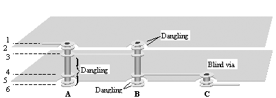
Through-hole vias that transition to and from the inner layers of a multi-layer board may leave vestigial sections hanging above or below the path of current (Figure 5.29).
Figure 5.29. Through-hole vias that transition to and from the inner layers may leave vestigial sections dangling above or below the path of current.
If a via is short compared to the signal risetime, you can still use a first-order lumped-element model, most likely an excess shunt capacitance. The entire capacitance of the via becomes C V , while the inductance only of the inner section, where signal current actually flows, makes up L V . From these values you may calculate C EXCESS .
If the via is too long, however, the dangling section can develop a resonance, exacerbating the effects of its capacitance. The pi-model is helpful in understanding and predicting this effect, although I will admit it is not clear precisely how to apportion the capacitance and inductance of the pi model among the three sections of the via (the central body section that carries signal current, an upper dangling section, and a lower dangling section).
The clearest example of via resonance involves a thick FR-4 backplane with press-fit connectors. Suppose the backplane is 6.35 mm thick (0.250 in.), and imagine a signal traversing the connector routes onto the backplane on the top layer ( nearest the daughter card). The entire length of the press-fit via, with the connector pin embedded in it, forms a dangling stub connected to the signal line at the point where the signal enters the backplane (see A in Figure 5.29). The minimum transit time, t v , through the stub structure approximately equals
Equation 5.33
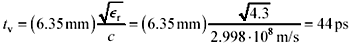
The dangling stub acts as an unterminated transmission line, generating a quarter-wave resonance (a zero) in impedance at a frequency corresponding to four times t v , or roughly 5.7 GHz. Any signal power near this resonant frequency will be seriously attenuated by the dangling via.
A pi-model of the same dangling stub would have shown a similar resonance at a frequency related to the combination of series inductance L V and the capacitance C V /2 at the far end of the structure, approximately ten percent lower (more conservative) than the quarter-wave stub theory would predict, with the exact value depending on how you calculate L V . In any structure where the current returns from the far end of the stub through the action of distributed displacement current the determination of L V is particularly difficult. Although neither model is perfect, they both draw your attention to the dangers of unterminated stubs.
If you find yourself worrying about precise models of stub resonance I suggest that you spend your time instead figuring out how to build smaller vias, or changing from binary signaling to a multi-level signal code that operates in a lower frequency band. Don't waste your life engineering the details of each and every via.
A blind via truncates the dangling stubs, producing a more compact structure with substantially less overall capacitance.
POINT TO REMEMBER
- A long, dangling via can develop a resonance, exacerbating the effects of its capacitance.
5.5.4 Capacitance Data
The following sections present three studies of via capacitance.
5.5.4.1 Three-Layer Via Capacitance
Brock J. LaMeres, in his BSEE thesis for Montana State University, simulated, using the Avant! Raphael 3D Field Simulator, a number of simple 3-layer via configurations (see Table 5.8, and the illustration in Figure 5.32). His simulations were then corroborated with physical measurements.
The 3-layer configuration represents the simplest form of via transition. There are only three layers, the top signal layer, the reference plane layer, and the bottom signal layer. At the position where the signal via penetrates the plane the returning signal current merely pops from one side of the solid reference plane to the other, passing through the clearance hole. In the three-layer configuration the series inductance of the via is negligible compared to its capacitance, suggesting the use of a simple lumped-element model of the excess-capacitance, a conclusion well supported by LaMeres' findings.
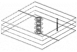
The capacitances were calculated in each case with the via standing in isolation, with no traces attached (see Table 5.8). The simulation software approximated each via pad, via body, and clearance hole with octagonal cylinders .
The dielectric spacing between layers 1 and 2, and also layers 2 and 3, was 18.9 mils. The thicknesses of the conductors on layers 1, 2, and 3 were all the same (2.2 mils), yielding an overall via length of 44.4 mils (from the top surface of layer 1 to the bottom surface of layer 3). The values of capacitance should be treated as approximate. The capacitance of a shorter via would be considerably less.
LaMeres also reports values of inductance for his vias, but these values are suspect, as they were developed using a model of one via standing in isolation and therefore do not take into account the presence of magnetic fringing fields from the associated traces. Inductance should be defined (and measured) using the technique of Section 5.5.1, "Incremental Parameters of a Via."
Table 5.8. Simulated Three-Layer Via Capacitance (LaMeres)
|
Drilled hole dia., mil |
Clearance dia., Mil |
Pad dia., mil |
Via length, mil |
Via capacitance C V pF |
|---|---|---|---|---|
|
18 |
46 |
20 |
44 |
0.23 |
|
18 |
46 |
30 |
44 |
0.31 |
|
18 |
46 |
40 |
44 |
0.46 |
|
12 |
36 |
20 |
44 |
0.21 |
|
12 |
36 |
30 |
44 |
0.31 |
|
12 |
36 |
40 |
44 |
0.46 |
|
8 |
28 |
20 |
44 |
0.19 |
|
8 |
28 |
30 |
44 |
0.30 |
|
8 |
28 |
40 |
44 |
0.46 |
|
NOTEData summarized from Brock J. LaMeres, Characterization of a Printed Circuit Board Via , B.S.E.E., Montana State University Technical Report EAS_ECE_2000_09, 1998 [48] |
||||
The data in Table 5.8 may be extrapolated to other via sizes (like buried vias). If all the specifications for a via (drilled hole, pad, clearance, length, and interplane spacing) are scaled by a factor k , the capacitance and inductance of the resulting configuration also scale by the same factor k . The capacitance also scales in proportion to the dielectric constant of the pcb material. The dielectric constant of the substrate assumed in Table 5.8 is 4.3.
5.5.4.2 Effect of Back-Drilling
In the event that your signal happens to traverse only layers 1 and 3, you might wonder if it is possible to cut off the dangling bottom section of the via, thus reducing its capacitance. This is possible in three ways:
- The buried-via process drills and plates various sublayers of a pcb before final board lamination, making possible the existence of miniature vias penetrating only partway through the board stack.
- The micro-via process laser-ablates through only a very thin dielectric separating the outermost two layers of a pcb. The finished structure is equivalent to a buried-via process with holes penetrating from the surface layer inward. Micro-vias may also be called blind vias .
- Finished plated-through-hole (PTH) vias may be back-drilled after plating . This secondary process uses a drill bit slightly larger than the original drill bit used to form the via hole. The back-drilling bit penetrates from the back side of the board partway through. This process cuts away the metallized surface of the via wall from the back side of the board, leaving a conductive structure that penetrates from the top surface only partway through the board.
Table 5.9 lists the capacitances of large through-hole vias that have been back-drilled. These vias are used with press-fit connectors in very thick, high-speed backplanes with multiple solid reference planes. The total backplane thickness in these examples was 250 mils. The via length was modified by progressively back-drilling the via to shorten the plated length of the hole. Your results vary according to the configuration of reference planes within the board.
The data in Table 5.9 may be extrapolated to other via sizes. If all the specifications for a via (drilled hole, pad, clearance, length, and interplane spacing) are scaled by a factor k , the capacitance of the resulting configuration also scales by the same factor k . The capacitance also scales in proportion to the dielectric constant of the pcb material. The dielectric constant of the substrate assumed in Table 5.9 is approximately 4.
Table 5.9. Change in Via Capacitance Due to Back-Drilling
|
Drilled hole dia., mil |
Plated hole dia., mil |
Clearance dia., mil |
Pad dia., mil |
PTH length, mil |
Via capacitance pF |
|---|---|---|---|---|---|
|
26 |
22 |
52 |
38 |
250 |
2.4 |
|
26 |
22 |
52 |
38 |
200 |
2.0 |
|
26 |
22 |
52 |
38 |
225 |
1.8 |
|
26 |
22 |
52 |
38 |
150 |
1.5 |
|
26 |
22 |
52 |
38 |
125 |
1.3 |
|
26 |
22 |
52 |
38 |
100 |
1.0 |
|
NOTE( The data in this table were adapted from Teradyne [43] ) |
|||||
Example estimation of via capacitance
Assume a via with these dimensions (all values in mils):
9
finished hole size (irrelevant to electrical properties)
13
drilled hole size (this sets the diameter of the outer wall of the via)
19
pad diameter
26
clearance diameter
63
via length
The ratio of via length to pad diameter for this example via most closely matches row 5 of Table 5.9. It differs from the via in row 5 by a scale factor of 1/2.
The capacitance listed in row 5 is 1.3 pF. The estimated capacitance of the example via should therefore be reduced from row 5 by your scale factor of 1/2 to a value of 0.65 pF.
To more accurately estimate the capacitance of a via, you should use a 3-D field solver.
5.5.4.3 Effect of Multiple Planes
The total capacitance of a via depends on the geometry of the via, the surrounding reference planes, the trace width used to connect to the via, and the dielectric constant of the substrate material. The capacitance does not depend (much) on which particular layers are used to interconnect traces leading to and from the via.
For example, suppose in a 14-layer board a certain through-hole via accepts a signal coming in on layer 1 and leaving on layer 3. An identical adjacent via accepts a signal coming in on layer 1 and leaving on layer 14. Even though the signal current traverses different sections of the two vias, the voltages on the vias are the same in both cases, so the total incremental capacitance added to the traces is the same. Central to this analysis, of course, is the assumption that the full length of the via remains electrically short compared to the signal risetime and that the pads on all layers bear similar relationships to their respective reference planes.
Factors that do matter a great deal in the calculation of via capacitance include the number and positions of the reference planes.
The analysis of via capacitance presented in Tables 5.10A through 5.10D was by performed by Matt Hudale of Ansoft Corporation using the Ansoft Q3D Extractor Version 5. The via-capacitance data was extracted from field simulations using the technique described in Section 5.5.1.
The traces were 5-mils wide (approx. 70 ohms). Hudale measured the total capacitance of the combination of via and trace, and then subtracted out the capacitance of a trace of equivalent length (and with equivalent fringing fields at its start and finish points) to arrive at a final figure for the incremental capacitance added to the line by the presence of the via structure.
The simulated area of the planes was a block 0.216 in. on a side with the via located in the center. The traces were 0.108-in. long on the top layer, and 0.108-in. long on the bottom layer, extending in each case to the edge of the simulated planes. The via barrels, via pads, and clearance holes were simulated with octagonal cylinders as shown in Figure 5.30. The percentage error for convergence was set to 1% in all scenarios with the exception of the 2-plane geometry for which it was set to 0.5%. The dielectric constant was for all calculations was set to 4.4.
Figure 5.30. Matt approximated the parts of each via with octagonal cylinders.
The first three tables show computed results for pad diameters of 24, 30, and 36 mils, and clearance diameters of 24, 30, and 36 mils. Examination of the data indicated that the computed data formed a fairly flat surface when plotted against the pad and clearance diameters, so I interpolated this data to finer gradations, showing interpolated results at steps of 2 mils. The interpolation doesn't add any new information; it just makes it easier to use the tables.
All the vias listed in Tables 5.10A through 5.10D penetrate completely through the board. In each case the board includes top and bottom layers for signals, plus from two to six additional solid reference layers. Signal pads are always present on the top and bottom layers. The pads may be either present or stripped on the plane layers, as indicated in the tables. Stripping pads from the reference plane layers (see Figure 5.31) reduces the capacitance of a via, but increases the risk of a mechanical short between the via pad and the plane due to capillary movement of the plating solution between the dielectric layers. In cases where the pads are present on plane layers the size of the clearance holes obviously imposes a restriction on the maximum pad diameter. If the pads on reference layers are stripped, as one might do when squeezing the clearance holes to maintain continuity of the reference planes in a very dense design, the pad diameter may exceed the clearance diameter.
Figure 5.31. Stripping pads from the reference plane layers reduces the capacitance of a via, but increases the risk of a short between the via pad and the plane.
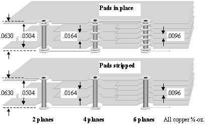
Table 5.10A. Via capacitance data for 0.063-in. board with TWO reference planes
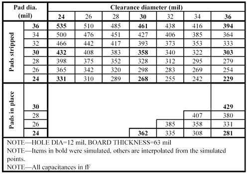
Table 5.10B. Via capacitance data for 0.063-in. board with FOUR reference planes
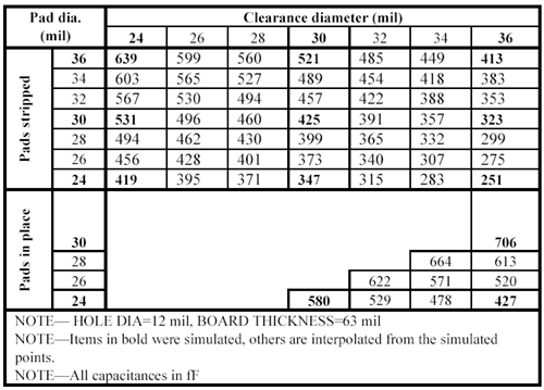
Table 5.10C. Via capacitance data for 0.063-in. board with SIX reference planes
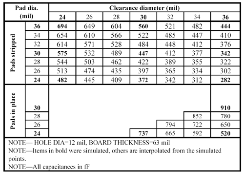
Table 5.10D. Via capacitance data for 0.096-in. board
|
Drilled hole dia., mil |
Pad dia., mil |
Clearance dia., mil |
Ref. planes |
Via cap. (fF) |
|
|---|---|---|---|---|---|
|
Pads stripped |
26 |
38 |
52 |
4 |
639 |
|
26 |
38 |
52 |
6 |
684 |
|
|
26 |
38 |
52 |
8 |
721 |
|
|
Pads in place |
26 |
38 |
52 |
4 |
784 |
|
26 |
38 |
52 |
6 |
934 |
|
|
26 |
38 |
52 |
8 |
1081 |
When only two reference-plane layers are used, they are located 5 mils below the top surface and 5 mils above the bottom surface of the board. When more reference-plane layers are used, the first two remain in the positions just described, and the others are spaced equally throughout the remaining interior of the board.
POINTS TO REMEMBER
- The incremental capacitance of a via is affected by the geometry of the via, the surrounding reference planes, the trace width used to connect to the via, and the dielectric constant of the substrate material.
- Via capacitance varies in proportion to the overall size of the via.
5.5.5 Inductance Data
5.5.5.1 Through-Hole Via Inductance
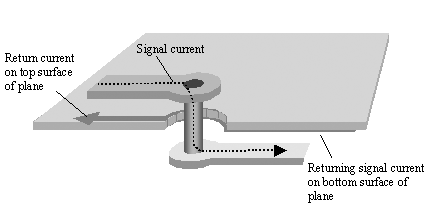
The inductance of a signal via depends on the location of the return path associated with that signal via. A signal via that traverses only one plane keeps the returning signal current close at hand all along the signal pathway (Figure 5.32). Where the signal via dives through the plane on a signal via, the return current dives through the clearance hole around the via onto the back side of the reference plane (at high frequencies the reference plane thickness exceeds the skin depth). The returning signal current flows only on the top or bottom surface of the reference plane; it does not penetrate the plane. The clearance hole around the signal via provides a portal through which the returning signal current can pop between top and bottom surfaces. To the left of the via the return current flows on the top surface of the reference plane, to the right it flows on the bottom surface. Such a signal via encounters almost no parasitic inductance; the effect of the via is primarily capacitive [48] . See also typical values in Table 5.8.
Figure 5.32. Returning signal current at a via pops between top and bottom surfaces of a solid reference plane by passing through the clearance hole.
The signal in Figure 5.33 traverses two reference planes. The returning signal current therefore must flow through the nearest available interplane connection. In Figure 5.33 the interplane connection is a via. The inductance of the overall configuration depends on the location of this interplane connection.
Figure 5.33. Returning signal current from the bottom surface of plane layer 3 pops through the lower clearance hole to the top surface of plane layer 3, then flows across the plane to the bottom of the interplane via, goes up that via to plane layer 2, then across the lower surface of plane layer 2 to the upper clearance hole, and finally pops through the upper clearance hole to the top surface of plane layer 2.
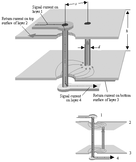
Keep in mind that at high frequencies the plane layers are many skin depths thickso thick that the returning signal current cannot penetrate the plane. It requires a hole in the plane to pop from one side to the other. Because the wall of a via is similarly thick, returning current does not generally flow down the hole on the inner surface of a via. It chooses to flow instead on the outside surface. The precise pathway of the returning current, including the exact place where it switches from the one surface of each plane to the other, is indicated in Figure 5.33. In a more complex configuration the returning signal current would spread out, penetrating several nearby clearance holes and using multiple nearby vias to accomplish the jump between layers 2 and 3.
If the planes are interconnected with one or more vias, the inductance becomes a function of the positions of all the nearby vias (see examples in Figure 5.34). If the signal changes reference planes from a ground plane to a power plane (or vice versa), the interplane path will include at least one capacitor. The inductance of the bypass capacitor above and beyond the topmost plane layer must be added to the interplane inductance computed per Figure 5.34. In a realistic situation with randomly placed interplane vias, the closest vias exert the lion's share of influence upon the overall inductance.
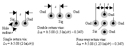
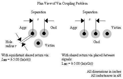
Figure 5.34. The inductance contributed by an interplane separation depends on the location of the nearest interplane connections. In all cases L V is the via interplane inductance (nH), r is the hole radius (in.), h is the spacing between the planes (in.), and s is the separation between via centers (in.). If the via traverses multiple plane layers, then h equals the aggregate distance traversed.
If you suspect that via inductance will play a significant role in your design, your choices are to (1) buy and learn to use a 3-D field solver, (2) prototype a stock set of geometries and catalog their performance for later use, or (3) build something (anything) and then adjust its geometry in successive passes until you get it right. The most common via adjustments are as follows :
- For large vias, back-drill the holes. This removes part of the plated metal from the inside of the finished via, starting from the back side of the board and working back in. If your signal goes only partway through the board, this method can be effective. Back-drilling directly reduces C V , raising Z V .
- Change the size of the drilled hole. This works if you are dealing with a signal via that doesn't have to accommodate a fixed size of connector pin. Shrinking the hole size while leaving the clearance and pad unchanged will reduce C V and increase L V .
- Change the size of the clearance hole. This works only to the extent that you can maintain continuity of the planes in and among your field of vias. Increasing the clearance diameter decreases C V and increases L V .
- Change the pad diameter. A smaller pad decreases C V but doesn't have much effect on L V .
- Reducing the hole size, clearance size, and pad diameter all together in proportion doesn't much change anything. You need to change the ratio of the drilled hole to the clearance hole, or the pad to the clearance hole, to get much of an effect.
- Enlarge the clearance hole in a noncircular manner. For example, elongating the clearance (anti-pad) on the side facing the incoming trace creates an egg-shaped or elliptical hole. The enlargement decreases C V , thus raising Z V . The advantage of using an elongated clearance is that it helps reduce the via capacitance without affecting the spacing between adjacent vias on either side. In a tightly spaced row of vias this helps preserve the continuity of the reference planes between clearance holes [53] .
In all cases check with your pcb fabricator to ensure that they comply with your precise adjustments of the hole, pad, and clearance sizes. Pcb vendors , often without telling you, make last-minute changes to these parameters in an attempt to improve their finished board yield.
POINTS TO REMEMBER
- The inductance of a signal via depends on the location of the return path associated with that signal via.
- A signal via that traverses only one plane keeps the returning signal current close at hand all along the signal pathway.
- A signal via that traverses two reference planes forces returning signal current through the nearest available interplane connection.
- If a signal changes reference planes from a ground plane to a power plane (or vice versa), the interplane return path must traverse bypass capacitors.
- Pcb vendors, often without telling you, make last-minute changes to hole, pad, and clearance sizes in an attempt to improve their finished board yield.
5.5.5.2 Via Crosstalk
This section concerns crosstalk generated by signals that traverse a stripline cavity (i.e., the space between any two solid reference planes).
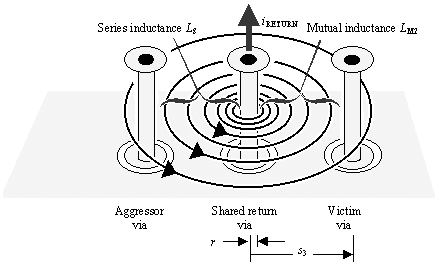
Figure 5.35 illustrates a typical scenario for two signal vias (aggressor and victim) that traverse the same cavity. The height of the cavity (spacing between the planes) is marked h .
Figure 5.35. Magnetic fields from the aggressive signal cause crosstalk.
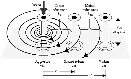
Signal current on the aggressor via creates patterns of magnetic fields within the cavity that look like concentric circles. The field intensity is constant in the z -axis direction (up and down in the figure), but drops off with 1/ x at distances removed from the aggressive trace. For a signal current of 1 amp, the magnetic field intensity B at a point within the cavity removed by distance x away from the signal via is
Equation 5.34

|
where |
m is the magnetic permeability of the dielectric substrate (H/m), |
|
x is the horizontal distance from the signal via, and |
|
|
for nonmagnetic substrate materials, m = 4 p 10 7 H/m. |
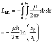
The mutual inductance L M1 from the signal current to the victim via is determined by integrating [5.34] over a range of x from s 1 (the distance from the signal via to the shared-return via) to s 2 (the distance from the signal via to the victim via), and also over the range of z from 0 to h . Taking into account the polarity of the coupling,
Equation 5.35
|
where |
m is the magnetic permeability of the dielectric substrate (H/m), |
|
s 1 is the horizontal distance from the signal via to the shared-return via (m), |
|
|
s 2 is the horizontal distance from the signal via to the victim via (m), |
|
|
h is the separation between the reference planes (m), and |
|
|
for nonmagnetic substrate materials, m = 4 p 10 7 H/m. |
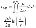
The mutual inductance L M2 from the aggressive return current to the victim via must also be taken into account (Figure 5.36). This inductance is determined by integrating [5.34] over a range of x from r (the radius of the shared-return via) to s 3 (the distance from the shared-return via to the victim via), and also over the range of z from 0 to h .
Figure 5.36. The return current, being closer to the victim than the signal path, causes even more crosstalk than does the signal current.
Equation 5.36
|
where |
m is the magnetic permeability of the dielectric substrate (H/m), |
|
s 3 is the horizontal distance from the shared-return via to the victim via (m), |
|
|
r is the radius of the shared-return via (m), |
|
|
h is the separation between the reference planes (m), and |
|
|
for nonmagnetic substrate materials, m = 4 p 10 7 H/m. |
The overall mutual inductance between the aggressive path (signal and return) and the victim path is the sum of [5.35] and [5.36].
Equation 5.37
|
where |
m is the magnetic permeability of the dielectric substrate (H/m), |
|
s 1 is the horizontal distance from the signal via to the shared-return via (m), |
|
|
s 2 is the horizontal distance from the signal via to the victim via (m), |
|
|
s 3 is the horizontal distance from the shared-return via to the victim via (m), |
|
|
r is the radius of the shared-return via (m), |
|
|
h is the separation between the reference planes (m), and |
|
|
the last equation assumes for nonmagnetic substrate materials m = 4 p 10 7 H/m. |
In the configuration of Figure 5.36 the return current via, being closer to the victim than the signal via, causes the majority of the crosstalk.
In English units, equation [5.37] is rewritten
Equation 5.38
|
where |
s 1 is the horizontal distance from the signal via to the shared-return via (in.), |
|
s 2 is the horizontal distance from the signal via to the victim via (in.), |
|
|
s 3 is the horizontal distance from the shared-return via to the victim via (in.), |
|
|
r is the radius of the shared-return via (in.), |
|
|
h is the separation between the reference planes (in.), and |
|
|
this equation assumes a nonmagnetic substrate. |
Various simplifications of [5.38] are listed in Figure 5.37 and Figure 5.38. For example, the case L MC in Figure 5.37 sets s 1 = s 3 = s , and s 2 = 2 s .
Figure 5.37. Self-inductances and mutual inductances are easily computed for simple via configurations.
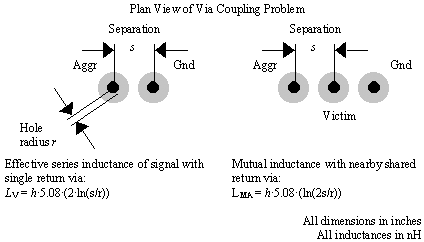
Figure 5.38. Mutual inductances are easily computed for simple via configurations.
Example calculation of mutual inductance of vias
Parameters:
- 20-mil pad
- 5-mil gap between pads
- h = 0.025
- r = 0.003
- s = 0.025
Self-inductance of via with single return path:
- L V = .539 nH = 3.38 W at 1 GHz
Mutual inductances from Figure 5.37 and Figure 5.38:
- L MA = .357 nH = 2.24 W at 1 GHz
- L MB = .269 nH = 1.69 W at 1 GHz
- L MC = .181 nH = 1.14 W at 1 GHz
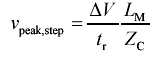
The crosstalk voltage induced in a victim circuit equals the rate of change of current in the aggressor times the mutual inductance, L M , shared between the two circuits. With a step change of aggressive current having a maximum rate of change equal to ( D V/Z C )/t r , the peak voltage in the victim circuit equals
Equation 5.39
For a sinusoidal excitation of amplitude a the maximum rate of change in the aggressor current equals ( a2 p f )/ Z C , for a peak victim voltage of
Equation 5.40
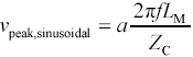
A mutual impedance of 2 p fL M = 1 W shared between two 50- W circuits therefore induces a crosstalk voltage in the victim of approximately 2%.
In a both-ends- terminated architecture, half of the inductively coupled crosstalk amplitude propagates towards either end of the victim circuit.
Within a group of signal vias that all share one common return path, the crosstalk from all the nearby aggressors aggregates.
POINTS TO REMEMBER
- Vias that traverse a common stripline cavity (i.e., the space between two reference planes) create crosstalk.
- The crosstalk voltage induced in a victim circuit equals the rate of change of current in the aggressor times the mutual inductance, L M , shared between the two circuits.
Fundamentals
- Impedance of Linear, Time-Invariant, Lumped-Element Circuits
- Power Ratios
- Rules of Scaling
- The Concept of Resonance
- Extra for Experts: Maximal Linear System Response to a Digital Input
Transmission Line Parameters
- Transmission Line Parameters
- Telegraphers Equations
- Derivation of Telegraphers Equations
- Ideal Transmission Line
- DC Resistance
- DC Conductance
- Skin Effect
- Skin-Effect Inductance
- Modeling Internal Impedance
- Concentric-Ring Skin-Effect Model
- Proximity Effect
- Surface Roughness
- Dielectric Effects
- Impedance in Series with the Return Path
- Slow-Wave Mode On-Chip
Performance Regions
- Performance Regions
- Signal Propagation Model
- Hierarchy of Regions
- Necessary Mathematics: Input Impedance and Transfer Function
- Lumped-Element Region
- RC Region
- LC Region (Constant-Loss Region)
- Skin-Effect Region
- Dielectric Loss Region
- Waveguide Dispersion Region
- Summary of Breakpoints Between Regions
- Equivalence Principle for Transmission Media
- Scaling Copper Transmission Media
- Scaling Multimode Fiber-Optic Cables
- Linear Equalization: Long Backplane Trace Example
- Adaptive Equalization: Accelerant Networks Transceiver
Frequency-Domain Modeling
- Frequency-Domain Modeling
- Going Nonlinear
- Approximations to the Fourier Transform
- Discrete Time Mapping
- Other Limitations of the FFT
- Normalizing the Output of an FFT Routine
- Useful Fourier Transform-Pairs
- Effect of Inadequate Sampling Rate
- Implementation of Frequency-Domain Simulation
- Embellishments
- Checking the Output of Your FFT Routine
Pcb (printed-circuit board) Traces
- Pcb (printed-circuit board) Traces
- Pcb Signal Propagation
- Limits to Attainable Distance
- Pcb Noise and Interference
- Pcb Connectors
- Modeling Vias
- The Future of On-Chip Interconnections
Differential Signaling
- Differential Signaling
- Single-Ended Circuits
- Two-Wire Circuits
- Differential Signaling
- Differential and Common-Mode Voltages and Currents
- Differential and Common-Mode Velocity
- Common-Mode Balance
- Common-Mode Range
- Differential to Common-Mode Conversion
- Differential Impedance
- Pcb Configurations
- Pcb Applications
- Intercabinet Applications
- LVDS Signaling
Generic Building-Cabling Standards
- Generic Building-Cabling Standards
- Generic Cabling Architecture
- SNR Budgeting
- Glossary of Cabling Terms
- Preferred Cable Combinations
- FAQ: Building-Cabling Practices
- Crossover Wiring
- Plenum-Rated Cables
- Laying Cables in an Uncooled Attic Space
- FAQ: Older Cable Types
100-Ohm Balanced Twisted-Pair Cabling
- 100-Ohm Balanced Twisted-Pair Cabling
- UTP Signal Propagation
- UTP Transmission Example: 10BASE-T
- UTP Noise and Interference
- UTP Connectors
- Issues with Screening
- Category-3 UTP at Elevated Temperature
150-Ohm STP-A Cabling
- 150-Ohm STP-A Cabling
- 150- W STP-A Signal Propagation
- 150- W STP-A Noise and Interference
- 150- W STP-A: Skew
- 150- W STP-A: Radiation and Safety
- 150- W STP-A: Comparison with UTP
- 150- W STP-A Connectors
Coaxial Cabling
- Coaxial Cabling
- Coaxial Signal Propagation
- Coaxial Cable Noise and Interference
- Coaxial Cable Connectors
Fiber-Optic Cabling
- Fiber-Optic Cabling
- Making Glass Fiber
- Finished Core Specifications
- Cabling the Fiber
- Wavelengths of Operation
- Multimode Glass Fiber-Optic Cabling
- Single-Mode Fiber-Optic Cabling
Clock Distribution
- Clock Distribution
- Extra Fries, Please
- Arithmetic of Clock Skew
- Clock Repeaters
- Stripline vs. Microstrip Delay
- Importance of Terminating Clock Lines
- Effect of Clock Receiver Thresholds
- Effect of Split Termination
- Intentional Delay Adjustments
- Driving Multiple Loads with Source Termination
- Daisy-Chain Clock Distribution
- The Jitters
- Power Supply Filtering for Clock Sources, Repeaters, and PLL Circuits
- Intentional Clock Modulation
- Reduced-Voltage Signaling
- Controlling Crosstalk on Clock Lines
- Reducing Emissions
Time-Domain Simulation Tools and Methods
- Ringing in a New Era
- Signal Integrity Simulation Process
- The Underlying Simulation Engine
- IBIS (I/O Buffer Information Specification)
- IBIS: History and Future Direction
- IBIS: Issues with Interpolation
- IBIS: Issues with SSO Noise
- Nature of EMC Work
- Power and Ground Resonance
Points to Remember
Appendix A. Building a Signal Integrity Department
Appendix B. Calculation of Loss Slope
Appendix C. Two-Port Analysis
- Appendix C. Two-Port Analysis
- Simple Cases Involving Transmission Lines
- Fully Configured Transmission Line
- Complicated Configurations
Appendix D. Accuracy of Pi Model
Appendix E. erf( )
Notes
EAN: N/A
Pages: 163
