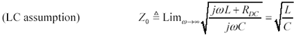
LC Region (Constant-Loss Region)
At higher frequencies the inductive reactance grows, eventually exceeding the magnitude of the DC resistance, forcing the line into the LC region (Section 3.2).
3.6.1 Boundary of LC Region
As illustrated in Figure 3.2, the LC region extends to all frequencies above frequency w LC . At that frequency the reactive component of the propagation coefficient ( w L ) equals in magnitude the resistive component ( R ).
Equation 3.83

|
where |
w LC is the lower limit of the LC region, rad/s, |
|
R DC is the series DC resistance of the transmission line (signal and return resistances added together), W /m, and |
|
|
L is the series inductance, H/m |
|
|
NOTE: |
For differential configurations, define R DC as the sum of the resistances of the outbound and returning conductors, and L as the inductance of the differential transmission line thus formed , L = Z DIFFERENTIAL / v DIFFERENTIAL . |
At all frequencies above w LC (including the skin effect, dielectric, and waveguide regions ) the line inductance plays a significant role in its operation and must be taken into account in system modeling.
If your maximum operating frequency exceeds w LC , but if at that frequency your transmission line length falls short of the boundary described by [3.25], then you may bypass any consideration of the peculiar properties of the LC region and use instead a lumped-element approximation (i.e., the pi model) to determine how your system will respond.
The distinguishing feature of the LC mode is that within this region the line attenuation does not much vary with frequency. Some transmission lines possess a broad, well-defined LC region in which the attenuation does not change over a wide band . Unfortunately, in the practical transmission lines used in most digital designs the LC region is relatively narrow (or sometimes nonexistent) so that the LC region shows up as nothing more than a subtle "flat spot" in the curve of attenuation vs. frequency, pinched between the RC region, where attenuation again grows with the square root of frequency, and the skin-effect region, where the attenuation grows with the square root of frequency (see Figure 3.1).
The narrowness of the LC region comes about because of the relationship between the external inductance and the internal inductance of a typical transmission-line configuration (see Section 2.8, "Modeling Internal Impedance"). The onset of LC mode happens at a frequency where the transmission line's total inductance (internal plus external) becomes significant compared to its resistance. The onset of the skin-effect mode, on the other hand, depends on the relation of only the internal inductance to the resistance. Because in most practical transmission lines used for digital applications the total cross-sectional area of the main TEM wave-carrying region exceeds the cross-sectional area of the signal conductor(s) by only a modest factor (on the order of 10 or less), the external inductance exceeds the internal inductance by a similar modest factor. The onset frequency of the skin-effect region therefore exceeds the onset of the LC mode by the same modest factor. Nevertheless, the study of pure LC-mode propagation serves as a useful gateway to the understanding of other regions.
To achieve a different result, you would have to use very thin conductors. For example, some twisted-pair and coaxial conductors are constructed from a high-permeability steel core surrounded by a thin layer of copper plating . The high permeability (and thus very shallow skin depth) of the steel core rejects all currents at even moderate frequencies, forcing all the current to flow in the thin copper-plated region. As long as skin depth of the copper region remains larger than the plating thickness , the line enjoys the benefits of a constant resistance over a wide band of frequencies. Such a transmission line has a generally increased, but very flat, loss in the LC region. This trick is used in some 1000BASE-CX Gigabit Ethernet shielded twisted-pair cables to flatten the loss characteristics of the cable, simplifying the equalization circuitry at each end.
POINTS TO REMEMBER
- The LC region begins where the magnitude of the line inductance ( w L ) exceeds the DC resistance ( R DC ).
- Within the LC region the line attenuation does not much vary with frequency.
- Unfortunately, in the practical transmission lines used in most digital designs the LC region is relatively narrow (or sometimes nonexistent).
3.6.2 Characteristic Impedance (LC Region)
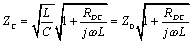
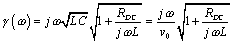
The full expression for characteristic impedance ( neglecting the conductance G ) includes contributions from both the inductance L and resistance R DC of the line.
Equation 3.84
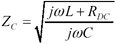
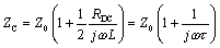
In the limit as you proceed to frequencies far above w LC , the contribution of the term R becomes negligible, leading to this approximation for characteristic impedance in the heart of the LC territory.
Equation 3.85
I name this parameter Z to distinguish it from the actual value of characteristic impedance Z C , which of course varies with frequency. At a frequency three times greater than w LC the difference in magnitude between Z and Z C is on the order of 5%. At a frequency 10 times higher than w LC the difference is on the order of 0.5%. Near w LC the value of [3.84] takes on a substantial phase angle and varies noticeably.
The general relationship between the characteristic impedance and input impedance of a transmission structure is given by [3.33] and discussed in Section 3.5.2, "Input Impedance (RC Region)," and in Section 3.2.1 "A Transmission Line Is Always a Transmission Line."
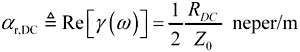
Figure 3.16 illustrates the transition in impedance between RC and LC modes for a hypothetical pcb trace. This figure takes into account only the DC resistance, capacitance , and inductance of the trace (i.e., it ignores both skin effect and dielectric losses). The trace is a 50-ohm stripline constructed of 1/2-oz copper (17.4 micron thickness) on FR-4 with a width of 150 microns (6 mils, v = 1.44610 8 m/s, L = 346 nH/m, C = 138 pF/m).
Figure 3.16. The characteristic impedance of an LC line asymptotically approaches Z at frequencies above w LC .
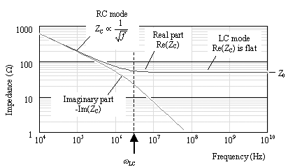
At frequencies below w LC (3 MHz in this example) both real and imaginary parts of the characteristic impedance vary with the inverse square root of frequency. Above w LC the imaginary part goes to zero and the overall impedance flattens out to approach a high-frequency asymptote of  , which in this case equals 50 W .
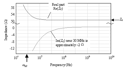
Figure 3.17 magnifies the region near the LC-mode transition, showing on a linear scale both real and imaginary parts of the characteristic impedance. A decade above w LC the impedance magnitude has moved to within a tiny fraction of 50 ohms; however, the characteristic impedance at this point (30 MHz) still carries an imaginary quantity of about 2 ohms. In absolute terms this imperfection represents a 4% variation from 50 ohms, which will lead to a 2% reflection coefficient if the line is sourced (or terminated ) with a pure 50-ohm resistance.
Figure 3.17. One decade above w LC the imaginary part of Z C carries a value of approximately 2 W .
POINTS TO REMEMBER
- At frequencies far above w LC the characteristic impedance of a pure LC-mode transmission line asymptotically approaches
 .
. - At a frequency ten times greater than w LC the complex value of characterisitic impedance differs from Z by only about 4%.
3.6.3 Influence of Series Resistance on TDR Measurements
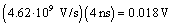
Figure 3.18 displays the TDR response of the same hypothetical pcb trace used in previous figures. The response begins with a half- sized step, persisting for one round-trip delay, after which the response rises to a full level. The trace length of 0.5 meters creates a round-trip delay of approximately 7 ns.
Figure 3.18. Series resistance tilts the TDR steps.
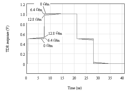
The series resistance present within the trace tilts the TDR steps. The values of DC resistance represented in Figure 3.18 are 0, 6.4, and 12.8 W /m (0, 0.163 and 0.325 W /in.), corresponding to stripline widths in 1/2-ounce copper of infinity, 150 m m, and 75 m m, (  , 6, and 3 mils) respectively. The greater the series resistance of the trace, the greater the tilt it induces in the TDR response. You can predict the degree of tilt from an analysis of the characteristic impedance.
At frequencies just above w LC the characteristic impedance of the trace in response to a step edge can be modeled as a resistance Z that trends gradually upward over time. This conclusion may be extracted from [3.85] by first factoring out from under the radical the asymptotic impedance Z , which by definition equals  .
.
Equation 3.86
Next use a first-order Taylor-series approximation for the remaining square root. This approximation is valid only at frequencies well above w LC .
Equation 3.87
|
where |
the time constant |
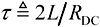 .
.Converting [3.87] to an expression that is a function of time shows that in response to a step input of current, the characteristic impedance of the line can be approximated in its first moments ( t << 2 L / R DC ) as an initial value equal Z followed by a gradual up-trend in impedance:
Equation 3.88
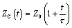
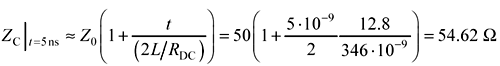
Example Calculation of Impedance Slope
Let Z = 50 W , L = 346 nH/m, and R DC = 12.8 W /m.
In response to a step input of current, the initial apparent impedance is Z = 50 W . At a time 5 ns after the initial step edge, the apparent impedance has increased to
The trend in impedance differs slightly from the trend in the TDR voltage, because the TDR setup delivers an input that comes not from a perfect current source, but from a source with finite impedance R S .
Given model [3.88] for the effective input impedance of an LC-mode transmission line in response to a step of current, you can relate the slope dx/dt of the slanted sections in a TDR waveform x ( t ) to the series resistance R DC of the transmission structure.
Equation 3.89
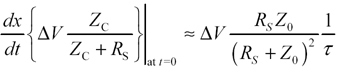
|
where |
dx/dt is the slope of the slanted section of the TDR response (V/s), |
|
D V is the open -circuit step-size of the TDR output (V), |
|
|
R S is the source impedance of the TDR instrument (usually 50 ohms), |
|
|
Z is the high-frequency asymptote for characteristic impedance (ohms) equal to |
|
|
t is a time constant defined equal to 2L/R DC , and |
|
|
R DC is the series DC resistance of the line (not taking into account skin effect). |
 ,
,Be forewarned that [3.89] applies only when the resistance R DC remains fixed and does not vary with frequency. In cases where the series resistance of the line varies significantly over the time interval of interest, as it would for example in consideration of the skin effect, then the AC value of skin-effect resistance must be used in the estimation of t and in the calculation of [3.89].
Example Calculation of TDR Slope
Let Z = 50 W , L = 346 nH/m, and R DC = 12.8 W /m.
With a 50- W TDR apparatus having a 1-V open-circuit output voltage, the apparent slope in the TDR waveform is
In a period of 5 ns you would expect the TDR waveform to creep upwards by
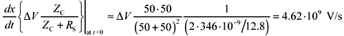
This amount agrees with the plot in Figure 3.19.
Figure 3.19. The inexorable upward creep of the TDR response causes measurements taken with slower risetimes to indicate slightly larger values of Z C ( R DC = 12.8 W /m).
By similar reasoning, a fixed conductance G creates a negative slope to the TDR waveform, with a time-constant  .
.
The last two figures in this section illustrate the effect of limited TDR risetime and the effect of a 50-ohm termination placed at the far end of the same line used in previous figures. The DC resistance in both cases equals 12.8 W /m. Figure 3.19 assumes risetimes of 35, 100, 350, and 1000 ps. Because of the sloping effect in the steps, measurements of impedance made with the smallest risetime reveal the smallest value of Z C . Slower measurements, to the extent that the step has time to drift upwards before a plateau in the driving waveform has been reached, tend to indicate slightly larger values. This figure highlights one of the difficulties of measuring characteristic impedance using the TDR method. Severe degrees of tilt make it very difficult to define one correct measurement procedure that is best for all applications.
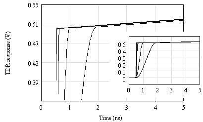
Figure 3.20 depicts the effect of a perfect 50-ohm load at the far end of the line. The end termination arrests the evolution of the sloped part of the TDR response, creating a perfectly flat top for all times beyond one round-trip delay.
Figure 3.20. An end termination arrests the evolution of the tilted portion of the TDR response ( R DC = 12.8 W /m).
POINT TO REMEMBER
- A fixed series resistance induces an upward tilt in the TDR measurement, indicating a gradually increasing impedance at lower frequencies.
3.6.4 Propagation Coefficient (LC Region)
Figure 3.21 shows the propagation coefficient for a hypothetical pcb trace with fixed DC resistance, but no skin effect or dielectric loss. This figure plots the real and imaginary parts of the propagation coefficient versus frequency. The plot is drawn with log-log axes to highlight the polynomial relationships between portions of the curves.
Figure 3.21. Above w LC the real and imaginary parts of the propagation coefficient separate, decoupling the attenuation (real part) from the phase (imaginary part).
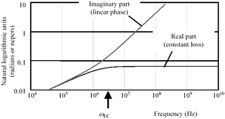
In the RC region below w LC both the real part of the propagation coefficient (log of attenuation) and the imaginary part (phase in radians) rise together in proportion to the square root of frequency. Within the RC region the attenuation and phase are coupled together in such a way that any line with a significant phase shift also naturally inherits a significant attenuation. It is therefore impossible to construct a passive high-Q resonator from an RC-mode transmission line without adding reactive components to the ends of the line.
In the LC region above w LC the situation changes. There is no longer any coupling between attenuation and phase within the LC region. In this region the imaginary part (phase) grows linearly with increasing frequency, while the real part (attenuation) stays fixed. It is quite possible within this region to construct a line with an enormous phase delay and yet very low attenuation. Such a line makes a terrific high-Q resonator. The existence of such resonant structures is the fundamental reason why terminations are so often needed on pcb traces used in high-speed applications.
At frequencies far above the LC mode boundary w LC the imaginary part of g approaches a linear-phase ramp equal to  , while the real part of g stabilizes at a constant value equal to R DC /(2 Z ). This conclusion is derived from [3.13] by first factoring out from under the radical a factor of j w , and also the inverse of propagation velocity v , defined as
  .
.
Equation 3.90
Next approximate the remaining square root. This approximation is valid only at frequencies well above w LC .
Equation 3.91
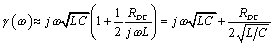
Substituting  leads to the aforementioned conclusion.
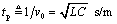
The linear-phase term implies that the one-way propagation function H of an LC-mode transmission line, for frequencies above w LC , acts mostly as a large time-delay element. The bulk propagation delay in units of seconds per meter is given by
Equation 3.92
Equation [3.92] may also be stated in terms of the effective relative permittivity  re associated with the transmission line configuration
 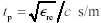 , assuming the speed of light c = 2.99810 8 m/s and further assuming the relative magnetic permeability m r equals one (see [2.28]).
The linear-phase property, in conjunction with the constant-loss property, implies that the one-way propagation function H of an LC-mode transmission line, for frequencies above w LC , acts as nothing more than a simple time-delay element with a fixed attenuation. The delay varies in proportion to the length of the transmission line. Doubling the length doubles the delay.
The transfer loss in nepers per meter is given by the real part of the propagation function. This value is called the resistive loss coefficient (note that this definition takes into account only the DC resistanceconsideration of the skin-effect resistance will increase actual line losses):
Equation 3.93
Equation 3.94
The low-pass filtering action of the skin effect implies that the step response will be dispersed, slurring crisp rising edges into edges of limited rise and fall time, according to the properties of the filter.
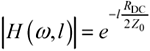
The magnitude of H is determined from the real part of the propagation function (see [2.16]):
Equation 3.95
|
where |
H ( w ,l ) is the magnitude of the line attenuation implied by [3.91] (this term does not vary with frequency), |
|
l is the length of the transmission line in meters, |
|
|
R DC is the DC resistance of the line, and |
|
|
Z is the high-frequency asymptotic characteristic impedance of the line. |
The signal loss represented by H , measured in nepers (or decibels), varies in proportional to the length of the transmission line. Double the distance yields twice the loss in neper or decibel units (one neper equals 8.6858896 dB).
The properties in Table 3.5 hold only for LC-mode transmission lines operated at frequencies well above w LC . Also note that R DC represents only the DC resistance of the line. Subsequent sections discuss the implications of the skin effect, which increases the total line resistance at high frequencies, and dielectric loss, which can further increases line attenuation.
POINTS TO REMEMBER
- The propagation function for an LC-mode transmission line is a simple delay with a fixed attenuation.
- Doubling the length of an LC-mode transmission line doubles the delay, and doubles the attenuation (in dB).
Table 3.5. Summary of LC Transmission Line Properties at Frequencies Well Above w LC
|
Property |
Formula |
Ref. Equation |
|---|---|---|
|
Asymptotic value of characteristic impedance |
|
[3.85] |
|
Bulk transport delay per meter |
|
[3.92] |
|
Attenuation in nepers per meter (1 neper = 8.6858896 decibels) |
|
[3.93] |
|
Attenuation in decibels per meter |
|
[3.94] |
|
Transfer gain at length l |
|
[3.95] |
|
Inductance per meter |
|
[3.5] |
|
Capacitance per meter |
|
[3.6] |


3.6.5 Possibility of Severe Resonance within the LC Region
In the LC region it is possible for a signal traveling on a long transmission line to accumulate a substantial amount of phase delay without suffering much attenuation. This property indicates that a transmission line may in certain circumstances act as an extremely high-Q resonant circuit.
Figure 3.22 illustrates the resonance associated with a hypothetical pcb trace having a fixed DC resistance, but no skin effect or dielectric loss. The trace is driven at the near end by a driver having a source impedance of 0, 10, or 20 ohms and left open-circuited at the far end. All LC transmission lines exhibit similar resonant peaks when driven by a source impedance less than Z . The peaks are located at frequencies (in Hertz) equal to odd multiples of l /(4 v ).
Figure 3.22. An LC line driven with a low-impedance source exhibits resonance at odd multiples of l /(4 v ) Hz.
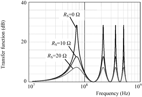
The heights of the peaks are limited partly by the series resistance of the line and partly by the damping effect of the source impedance at the driver. The greater the source impedance of the driver, the greater its damping effect on the circuit. Because in this example only the DC resistance of the line is taken into account (i.e., ignoring skin effect and dielectric effects), all the peaks occur at the same height.
The peaks are predicted by Equation [3.17]. In the present case involving an open-circuited (i.e., non-loaded) transmission line this equation may be simplified by eliminating from the denominator all terms involving Z L .
Equation 3.96
In the case of a very low source impedance ( Z S  0) the main difficulty with this equation is the cancellation that occurs within the term H 1 + H . Figure 3.23 shows how this cancellation can occur. The figure plots the trajectories of H and H 1 on the complex plane as a function of frequency. For a line with a lot of phase delay but not much attenuation, the trajectory of H remains at almost unit magnitude as it spirals clockwise around the origin. The trajectory of H 1 describes a similar path , spiraling counterclockwise just outside the unit circle. As H approaches j , and H 1 at the same frequency approaches + j , the average value of the two functions passes close to zero. In the absence of any significant source impedance Z S , when the first term in the denominator of G OPEN passes close to zero, the function G OPEN spikes upward, forming a sharp resonant peak.
Figure 3.23. As the trajectories of H 1 and H approach +j and -j , the average value [ H 1 + H ]/2 passes close to the origin.
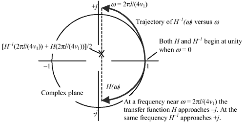
In the RC transmission mode such a resonance cannot happen. In the RC mode the real and imaginary parts of the propagation coefficient are always equal so that a phase of - p /2 must always be accompanied by an attenuation of e - p /2 = 0.208. The attenuation of H (and amplification of H 1 ) prevents the average of H and H 1 from passing close to the origin.
In the LC mode, it is the contribution of Z S that pushes the denominator at f = l /(4 v ) up and away from the origin, damping the resonance.
If a current-source driver (high source impedance) is used, similar resonance effects occur but at even multiples of f = l /(4 v ).
3.6.5.1 Alternate Interpretation of Equation [3.17]
Equation [3.17] may be algebraically manipulated into the following form:
Equation 3.97
|
where |
G is the overall system gain from the open-circuited output of the driver v 1 to the load v 3 , |
|
|
|
|
|
|
|
H is the one-way propagation function of the raw, unloaded transmission structure [3.14]. |
 is the reflection coefficient at the source end of the transmission structure,
 is the reflection coefficient at the load end of the transmission structure, and
This formulation makes clear the relation between the one-way propagation function H , the reflection coefficients G 1 and G 2 , and the height of the resonant peaks in the overall system gain G . Assume for the moment that the reflection coefficients are large quantities (near unity) that do not vary strongly with frequency. Under that assumption the overall gain is determined mostly by action of the denominator (1 H 2 G 1 G 2 ). If H can acquire a large phase shift without much attenuation, then the possibility exists that it will (at some frequency) pass very close to zero, causing a large spike in the overall system gain G .
Appropriate remedies for the resonance include
- Design a load impedance Z L such that G 2 is at all frequencies limited in magnitude, or
- Design a source impedance Z S such that G 1 is at all frequencies limited in magnitude, or
- Do both (1) and (2).
These remedies correspond to the end, source, and both-ends termination strategies, respectively, outlined in Section 3.6.6.
3.6.5.2 Practical Effect of Resonance
In all cases please remember that any LC resonance affects only signals whose bandwidth extends into the resonant region. As long as the knee frequency [3.19] of your digital logic falls well below the first resonance, the LC-resonance effects won't significantly distort your signal. This condition is effectively the same as condition [3.27] for lumped-element operation.
POINTS TO REMEMBER
- In the LC region a signal can accumulate a substantial amount of phase delay without suffering much attenuation. This property indicates that a transmission line can act as an extremely high-Q resonant circuit.
- LC-mode resonance affects only signals whose bandwidth extends into the resonant region.
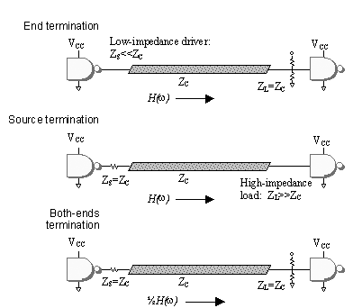
3.6.6 Terminating an LC Transmission Line
As explained in the previous section, the overall circuit gain G of a long transmission-line configuration can differ substantially from H , where H represents the one-way attenuation of signals moving from end to end across the transmission line. Even in cases where H is relatively well-behaved, the overall circuit performance can sometimes suffer from terrible resonance.
There are three classic ways to stabilize the propagation function of an LC transmission line, eliminating the undesirable resonance. Each case uses a resistive termination to deliver a circuit gain proportional to the one-way transmission line propagation function H ( w ) (see [3.14]). In the case of a relatively short LC transmission line (such as normally used on a printed-circuit card for high-speed digital signals) the propagation function H is practically flat with linear phase, indicating the line itself acts as nothing more than a time-delay element with a minor amount of attenuation.
Presuming that the attenuation (and possibly distortion) of H ( w ) falls within acceptable bounds, a properly terminated LC-mode transmission line may be operated satisfactorily at any length.
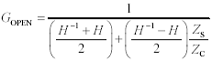
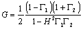
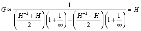
The three classic termination styles appear in Figure 3.24. The overall circuit gain G for each is derived from [3.17], repeated here for convenience.
Figure 3.24. The end, source, and both-ends termination schemes each deliver a system response nearly proportional to H ( w ).
Equation 3.98
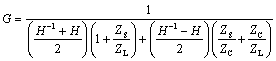
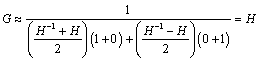
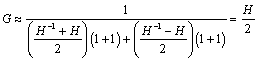
3.6.6.1 End Termination
Assuming a load impedance [24] Z L reasonably close to Z C , you may substitute 1 for the expression Z C / Z L in [3.17]. Further assuming a source impedance Z S much less than Z C , you may ignore the terms Z S /Z L and Z S /Z C in [3.17]. With these simplifications made, the expression for the overall circuit gain of an end-terminated transmission line reduces to
[24] The load is assumed connected to ground. Connection of the load impedance to any other voltages requires a superposition of the solution given here with a second static solution related to the applied termination voltage.
Equation 3.99
3.6.6.2 Source Termination
Assuming a source impedance Z S reasonably close to Z C , you may substitute 1 for the expression Z S / Z C in [3.17]. Further assuming a load impedance Z L much larger than Z C , you may ignore the terms Z S / Z L and Z C / Z L in [3.17]. With these simplifications made, the expression for the overall circuit gain of a source-terminated transmission line reduces to
Equation 3.100
3.6.6.3 Both-Ends Termination
Assuming source and load impedances to be the same, you may substitute 1 for the expression Z S / Z L in [3.17]. Further assuming both impedances to be reasonably close to Z C , you may substitute 1 for both expressions Z S / Z L and Z C /Z L in [3.17]. With these simplifications made, the expression for the overall circuit gain of a source-terminated transmission line reduces to
Equation 3.101
3.6.6.4 Subtle Differences Between Termination Styles
The three termination styles react differently to the presence of line resistance. Figure 3.25 shows those differences. All cases depict a hypothetical pcb trace having a fixed DC resistance of 6.4 W /m but no skin effect or dielectric loss. The trace is a 50-ohm stripline constructed of 1/2-oz copper (17.4 micron thickness) on FR-4 with a width of 150 microns (6 mils, v = 1.44610 8 m/s, L = 346 nH/m, C = 138 pF/m). The trace length l = 0.5 meters. The response of the both-ends terminated circuit has been artificially multiplied by two, raising its output to a level comparable with the other two plots for display purposes.
Figure 3.25. Different termination styles react differently to a fixed line resistance.
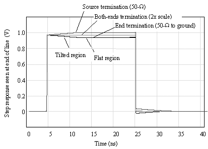
In all cases the initial step amplitude is the same, corresponding to the circuit gain at high frequencies given by [3.93]. At DC, however, the responses differ.
In the source-terminated case there is no load at the far end of the line to draw any DC current, so the final value of current within the transmission line is zero, and the steady-state voltage drop from end to end across the transmission line must also be zero. The final value of the circuit output at the far end of the line therefore begins at a point defined by [3.93] and then drifts up to the full open-circuit voltage of the source (in this case, 1.0 volts ).
In the end-terminated case the load at DC draws a substantial current. The attenuation at DC depends on the relation between the load impedance and the total series impedance of the line:
Equation 3.102
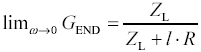
|
where |
G END is the overall circuit gain of an end-terminated transmission line with one-way propagation function H , |
|
Z L is the load impedance applied to the end of the line, |
|
|
the source impedance Z S is assumed much smaller than the characteristic impedance of the line Z C , |
|
|
the line length is l (m), and |
|
|
R is the transmission line series resistance per meter ( W /m). |
The value [3.102] is always less than the circuit gain predicted by [3.93]. The circuit output at the far end of the line therefore begins at a point defined by [3.93] and then drifts down to the value indicated by [3.102].
In Figure 3.25 the total resistance of the trace ( l = 0.5 meters times 6.4 W /m) is 3.2 W , which amounts to 6.4% of the trace impedance. The steady-state amplitude of the end-terminated waveform is therefore reduced by a factor of 6.4%.
The both-ends terminated case is least sensitive to internal resistance. To first order, internal series resistance induces no tilt to the circuit output. The initial step amplitude and the final value of step amplitude of a both-ends terminated circuit are the same. [25]
[25] In a both-ends termination structure the difference between the upwards tilt of the TDR response at the head of the line and the progressive attenuation of an initial step edge as it propagates down the same line is just enough to ensure that by the time your initial step edge reaches the end, a satisfactory steady-state condition has been reached with the far end voltage a little less than 50% [3.106] and the near-end voltage a little greater than 50%.
3.6.6.5 Application of Termination Equations to Other Regions
The LC, skin-effect, and dielectric-loss-limited regions all share the same asymptotic high-frequency value of characteristic impedance Z . The same termination approaches therefore work for all three regions, delivering in each case an overall circuit gain G equal to the one-way propagation function H applicable within each region.
Because the propagation function H is flat with frequency within the LC region, a well-terminated line operated within this region delivers a minor amount of attenuation but no distortion in the shape of the signal (i.e., no dispersion of the rising edge).
In the skin-effect and dielectric-loss-limited regions the propagation function H is not flat. It acts in these regions as a low-pass filter, attenuating and dispersing the edges of all signals passing through the transmission line.
POINTS TO REMEMBER
- The source, end, and both-ends terminations can all be used to eliminate LC-mode resonance.
- The end-termination is least sensitive to the series resistance of the transmission line.
3.6.7 Tradeoffs Between Distance And Speed (LC Region)
Given a fixed receiver architecture, and presuming that you remain within the LC region, the maximum speed of operation is not directly limited by transmission-line length. The tradeoff between length and speed disappears within the LC region because the attenuation (in dB) does not vary with frequency. A 10% increase in transmission-line length therefore increases the attenuation (in dB) by 10%. Such an increase in the attenuation of an LC-mode transmission line cannot be offset by a reduction in system operating speed.
POINT TO REMEMBER
- The speed of operation achievable within the LC region is not directly limited by transmission-line length.
3.6.8 Mixed-Mode Operation (LC and RC Regions)
Figure 3.26 illustrates the transmission line modes spanned by two systems, each represented by rays. System (A) operates at a length below the critical length l RC (see [3.54], under Section 3.5.1, "Boundary of RC Region"). At that length its frequency range of operation (0 to 20 MHz) spans only the LC and lumped-element regions. This system should be terminated with an impedance equal to the high-frequency characteristic impedance asymptote, Z . Any such terminator will likely continue to do an adequate job as the frequency of operation descends down into the lumped-element region. This is the normal arrangement for pcb tracesbefore you get down to a frequency low enough to observe RC effects, the whole system acts as a big lumped-element circuit anyway and (provided you don't have reactive loads) within the lumped-element region any old termination scheme will work.
Figure 3.26. The range of performance for some applications may span multiple regions.
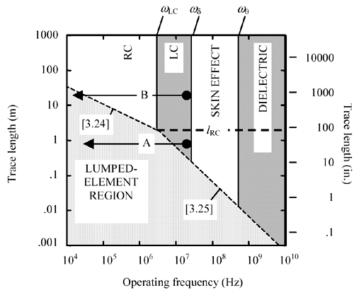
System (B) is quite different. It operates at a length greater than l RC . Its frequency range of operation is the same, but because of its greater length, its operational modes span the LC, RC, and lumped-element regions. The frequency response of this system will be a strong function of frequency (in the RC zone), so some form of equalization may be required. The ideal termination impedance for this system may be a frequency-varying network.
POINT TO REMEMBER
- Transmission lies operated at a length greater than l RC may display characteristics of both LC and RC behavior.
Fundamentals
- Impedance of Linear, Time-Invariant, Lumped-Element Circuits
- Power Ratios
- Rules of Scaling
- The Concept of Resonance
- Extra for Experts: Maximal Linear System Response to a Digital Input
Transmission Line Parameters
- Transmission Line Parameters
- Telegraphers Equations
- Derivation of Telegraphers Equations
- Ideal Transmission Line
- DC Resistance
- DC Conductance
- Skin Effect
- Skin-Effect Inductance
- Modeling Internal Impedance
- Concentric-Ring Skin-Effect Model
- Proximity Effect
- Surface Roughness
- Dielectric Effects
- Impedance in Series with the Return Path
- Slow-Wave Mode On-Chip
Performance Regions
- Performance Regions
- Signal Propagation Model
- Hierarchy of Regions
- Necessary Mathematics: Input Impedance and Transfer Function
- Lumped-Element Region
- RC Region
- LC Region (Constant-Loss Region)
- Skin-Effect Region
- Dielectric Loss Region
- Waveguide Dispersion Region
- Summary of Breakpoints Between Regions
- Equivalence Principle for Transmission Media
- Scaling Copper Transmission Media
- Scaling Multimode Fiber-Optic Cables
- Linear Equalization: Long Backplane Trace Example
- Adaptive Equalization: Accelerant Networks Transceiver
Frequency-Domain Modeling
- Frequency-Domain Modeling
- Going Nonlinear
- Approximations to the Fourier Transform
- Discrete Time Mapping
- Other Limitations of the FFT
- Normalizing the Output of an FFT Routine
- Useful Fourier Transform-Pairs
- Effect of Inadequate Sampling Rate
- Implementation of Frequency-Domain Simulation
- Embellishments
- Checking the Output of Your FFT Routine
Pcb (printed-circuit board) Traces
- Pcb (printed-circuit board) Traces
- Pcb Signal Propagation
- Limits to Attainable Distance
- Pcb Noise and Interference
- Pcb Connectors
- Modeling Vias
- The Future of On-Chip Interconnections
Differential Signaling
- Differential Signaling
- Single-Ended Circuits
- Two-Wire Circuits
- Differential Signaling
- Differential and Common-Mode Voltages and Currents
- Differential and Common-Mode Velocity
- Common-Mode Balance
- Common-Mode Range
- Differential to Common-Mode Conversion
- Differential Impedance
- Pcb Configurations
- Pcb Applications
- Intercabinet Applications
- LVDS Signaling
Generic Building-Cabling Standards
- Generic Building-Cabling Standards
- Generic Cabling Architecture
- SNR Budgeting
- Glossary of Cabling Terms
- Preferred Cable Combinations
- FAQ: Building-Cabling Practices
- Crossover Wiring
- Plenum-Rated Cables
- Laying Cables in an Uncooled Attic Space
- FAQ: Older Cable Types
100-Ohm Balanced Twisted-Pair Cabling
- 100-Ohm Balanced Twisted-Pair Cabling
- UTP Signal Propagation
- UTP Transmission Example: 10BASE-T
- UTP Noise and Interference
- UTP Connectors
- Issues with Screening
- Category-3 UTP at Elevated Temperature
150-Ohm STP-A Cabling
- 150-Ohm STP-A Cabling
- 150- W STP-A Signal Propagation
- 150- W STP-A Noise and Interference
- 150- W STP-A: Skew
- 150- W STP-A: Radiation and Safety
- 150- W STP-A: Comparison with UTP
- 150- W STP-A Connectors
Coaxial Cabling
- Coaxial Cabling
- Coaxial Signal Propagation
- Coaxial Cable Noise and Interference
- Coaxial Cable Connectors
Fiber-Optic Cabling
- Fiber-Optic Cabling
- Making Glass Fiber
- Finished Core Specifications
- Cabling the Fiber
- Wavelengths of Operation
- Multimode Glass Fiber-Optic Cabling
- Single-Mode Fiber-Optic Cabling
Clock Distribution
- Clock Distribution
- Extra Fries, Please
- Arithmetic of Clock Skew
- Clock Repeaters
- Stripline vs. Microstrip Delay
- Importance of Terminating Clock Lines
- Effect of Clock Receiver Thresholds
- Effect of Split Termination
- Intentional Delay Adjustments
- Driving Multiple Loads with Source Termination
- Daisy-Chain Clock Distribution
- The Jitters
- Power Supply Filtering for Clock Sources, Repeaters, and PLL Circuits
- Intentional Clock Modulation
- Reduced-Voltage Signaling
- Controlling Crosstalk on Clock Lines
- Reducing Emissions
Time-Domain Simulation Tools and Methods
- Ringing in a New Era
- Signal Integrity Simulation Process
- The Underlying Simulation Engine
- IBIS (I/O Buffer Information Specification)
- IBIS: History and Future Direction
- IBIS: Issues with Interpolation
- IBIS: Issues with SSO Noise
- Nature of EMC Work
- Power and Ground Resonance
Points to Remember
Appendix A. Building a Signal Integrity Department
Appendix B. Calculation of Loss Slope
Appendix C. Two-Port Analysis
- Appendix C. Two-Port Analysis
- Simple Cases Involving Transmission Lines
- Fully Configured Transmission Line
- Complicated Configurations
Appendix D. Accuracy of Pi Model
Appendix E. erf( )
Notes
EAN: N/A
Pages: 163
