Proximity Effect
High-frequency current in a round wire flows mostly on the surface of the wire, but not in a uniform distribution around the perimeter. The magnetic fields from the wire and its associated return current distribute the current around the perimeter in a slightly nonuniform way (Figure 2.19), which in turn increases the apparent resistance of the conductors above and beyond what you would expect from the action of the skin effect alone. In parallel conductors we call this additional increase in resistance the proximity effect .
Figure 2.19. The proximity effect redistributes the high-frequency current around the perimeter of a conductor.
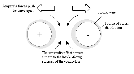
The proximity effect stands apart from the skin effect, which is what holds high-frequency current in a shallow band of depth d around the perimeter of a conductor (see previous section). The proximity effect also stands apart from Ampere's discovery that adjacent wires carrying opposing DC currents repel . While Ampere's forces push the atomic lattice structure of the two wires apart, and the skin effect binds current tightly to the surface, the proximity effect merely redistributes the AC current density around the perimeters of the two wires. The proximity effect exerts no net mechanical force on the wires.
The proximity effect is an inductive mechanism caused by changing magnetic fields. It perturbs the flow of high-frequency currents. It ignores steady currents that generate static magnetic fields. Above that frequency where the proximity effect takes hold, the distribution of current around the perimeter of the conductor attains a minimum-inductance configuration and does not vary further with frequency (until you reach the onset of non-TEM modes of propagation).
Figure 2.12 illustrates the magnetic fields within a single conductor, showing how self-induced eddy currents restrict the flow of current to a shallow band just underneath the surface of the conductor. The proximity effect operates by a similar mechanism. In the case of the proximity effect magnetic fields from a first wire induce eddy currents on a second wire, redistributing the current on the surface of a second conductor (Figure 2.20). The current on the second conductor is still bound tightly to a shallow band just underneath the surface by its own internal skin effect, but the proximity effect redistributes the current around the perimeter of the second conductor.
Figure 2.20. A changing magnetic field from a first conductor induces eddy currents on the surface of the second conductor, changing its distribution of current.
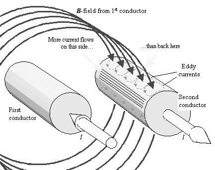
The diagram shows eddy currents circulating about the magnetic field, penetrating the top of the second conductor, and more eddy currents circulating on the bottom where the magnetic lines of force exit. The net effect of these eddy currents is to concentrate more current on the inside-facing surfaces of the conductors and less on the outward- facing sides. For a good conductor, at frequencies in excess of w d , the concentration builds until the magnetic field no longer penetrates the second conductor.
The skin effect and the proximity effect are two manifestations of the same principle: that magnetic lines of flux cannot penetrate a good conductor. The difference between the effects is that the skin effect is the reaction to magnetic fields generated by current flowing within the affected conductor, while the proximity effect is the reaction to magnetic fields generated by current flowing in other conductors . Both effects operate by the same guiding principle, namely, that no high-frequency magnetic fields shall penetrate the conductor. The frequency at which the proximity effect takes hold is therefore the same as that frequency w d where the skin effect takes hold. Figure 2.21 shows the pattern of magnetic lines of force surrounding two round conductors at a frequency well above w d . As you can see, the lines of magnetic force lie tangent to the surfaces of the conductors.
Figure 2.21. This cross-sectional view of the magnetic field in the vicinity of two round conductors shows the magnetic lines of force lie tangent to the surfaces of the conductors. Perturbations in the smoothness of the magnetic lines of force are articfacts of the spatial quantization used by a field solver to generate this diagram
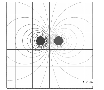
In any 2-D magnetic field picture the density of the magnetic lines of force indicates the strength of the magnetic field. Around the perimeter of the conductors, the density of current at a particular point on the surface of the conductor profile is proportional to the magnetic field at that point. In Figure 2.21 the magnetic lines of force clearly lie closer together on the inside-facing sides of the two conductors, indicating a preponderance of field intensity, and therefore current, on the inside-facing sides of the conductors.
2.10.1 Proximity Factor
The proximity factor represents the increase in the apparent AC resistance of conductors above and beyond what you would expect from the action of the skin effect alone. The proximity factor appears in the equation for AC resistance (see Section 2.6, "Skin Effect"):
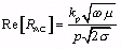
Equation 2.63
|
where |
k p is a correction factor determined by the proximity effect, |
|
the correction factor for the roughness effect is ignored, (see Section 2.11, "Surface Roughness"), |
|
|
w is the frequency of operation (rad/s), |
|
|
Re[R AC ] is the series resistance of the conductor taking into account both skin effect and proximity effect ( W /m), and assuming w >> w d , |
|
|
p is the perimeter of a cross-section of the signal conductor (m), |
|
|
m is the magnetic permeability of the conductor (H/m), and |
|
|
s is the resistivity of the wire (S/m). |
|
|
For annealed copper s = 5.800 ·10 7 S/m. |
|
|
For non-magnetic materials m = 4 p ·10 “7 H/m. |
|
The factor k p is technically defined as the ratio of (1) the actual AC resistance to (2) the resistance calculated assuming a uniform distribution of current around the perimeter of the signal conductor and ignoring the resistance of the return conductor.
The general behavior of k p is as follows .
- Any conductor well separated from a low-resistance return path has k p
 1.
1. - Differential configurations have k p 2 (and also k a 2).
- As the conductor and its return path are brought more closely together, k p increases.
- Whatever the value of k p , at frequencies below w d it has no effect on the transmission response; only the DC resistance matters at frequencies below w d .
For a pair of round wires, the magnitude of the proximity factor k p is determined by the ratio s / d , where s is the wire separation between centers and d is the wire diameter, as shown in Figure 2.22. At large ratios of s/d the proximity factor asymptotically approaches 2, representing the fact that in a twisted-pair cable the series resistance is always twice the resistance of a single wire alone. At a ratio of s / d = 2.0, corresponding roughly to the typical configuration of a 100-ohm twisted-pair cable, the proximity factor for round wires is 2.30. The proximity factor soars when the two wires almost touch.
Figure 2.22. The proximity factor for round wires increases as they are brought together. (Adapted from Frederick Terman, Radio Engineer's Handbook , McGraw-Hill, New York, 1943, p. 43).
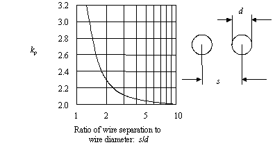
Figure 2.13 depicts for various conductors the frequency at which the skin and proximity effects take hold. For a conductor operating below its onset frequency, the magnetic forces due to changing currents in the conductor are too small, compared to the resistive forces, to influence the pattern of current flow. Low-frequency current therefore follows the path of least resistance . The path of least resistance fills the volume of every conductor, flowing uniformly throughout the cross section of the conductor.
Above the onset frequency, the magnetic forces, which grow in proportion to frequency, exceed the resistive forces, so it is the magnetic (inductive) effect that determines the path of current. Above the onset frequency, current flows in the path of least inductance .
The general principles of high-frequency current flow follow:
- Current in a conductor at high frequencies distributes itself to neutralize all the internal magnetic forces.
- At high frequencies magnetic lines of force will not penetrate a conducting surface.
- At high frequencies the lines of magnetic force flow tangent to every conducting surface.
- In more technical terms, the component of the magnetic field normal to a (good) conducting surface is (nearly) zero.
- Current at high frequencies distributes itself in that pattern which minimizes the total potential energy stored in the magnetic field surrounding the conductors.
- Current at high frequencies distributes itself in that pattern which minimizes the total inductance of the loop formed by the outgoing and returning current.
- Given a choice, returning signal current prefers to flow near the outbound signal path.
- In a high-speed pcb with a solid reference plane the return current for each signal flows on the underlying reference plane following closely underneath the signal trace.
All of the above viewpoints are correct, and they are all equivalent. The effective series resistance of a conductor in the zone far above w d is usually found using a tool called a 2-D electromagnetic field solver. Such tools calculate the proximity effect for conductors of arbitrary shape. Some hints about the operation of this class of tools is provided in Section 2.10.4.2, "2-D QuasiStatic Field Solvers."
Near the onset region, the exact interactions between the skin effect and proximity effect are not easily modeled . Most 2-D modeling software works well below the onset frequency where only the DC resistance matters. It also works well above the onset frequency where only the perimeter, skin depth, and proximity factor k p matter. Near the onset region, the software uses a generic mixing function to transition gradually from one mode to the other. The model is inexact near the transition region. In the modeling of typical pcb configurations this inaccuracy makes little difference, because the interesting problems usually occur well above the onset frequency. The differences between mixing functions are discussed in Section 2.8.1, "Practical Modeling of Internal Impedance."
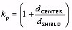
2.10.2 Proximity Effect for Coaxial Cables
Coaxial cables, owing to the concentricity of their conductors, exhibit a very simple distribution of high-frequency current. Around the center conductor the current is evenly distributed. Around the shield it is also evenly distributed albeit at a lower current density related to the ratio between the diameter of the center conductor and the diameter of the shield.
The calculation of k p takes into account the sum of series resistances of the signal conductor and the shield:
Equation 2.64
|
where |
d CENTER is the outside diameter of the center conductor (m), and |
|
d SHIELD is the inside diameter of the shield conductor (m). |
2.10.3 Proximity Effect for Microstrip and Stripline Circuits
Microstrip and stripline circuits fall subject to the proximity effect in the same way as circular conductors. The proximity effect draws signal current towards the reference plane-facing side of the (microstrip or stripline) trace, and simultaneously concentrates the returning signal current on the reference plane, forming it into a narrow band that flows on the plane, mostly staying underneath the signal trace.
Chapters 5 and 6 include tables of proximity factors for both single-ended and differential configurations.
2.10.4 Last Words on Proximity Effect
I shall close this section with two brief articles about the proximity effect. The first article outlines one algorithm for computing the proximity effect. This algorithm can be implemented in any general-purpose math spreadsheet. The second article concerns general limitations that apply to all 2-D simulators.
2.10.4.1 Proximity Effect II

2.10.4.2 2-D Quasistatic Field Solvers
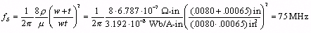
Article first published in EDN Magazine , September 27, 2001I love signal-integrity simulators. Unfortunately, they don't always produce the right answers. For example, most signal-integrity software packages calculate the impedance and loss of transmission lines using a 2-D, quasi-static, discrete field solver. The field solver depends on six crucial assumptions. If your system violates any of these assumptions, the simulator produces wrong answers. The Fringing-Field Assumption Two-dimensional field solvers do not calculate fringing fields at the ends of conductors. This omission seems reasonable as long as the main effects in the middle of the line vastly exceed the fringing-field effects at the ends. To satisfy this requirement, the length of a transmission line must vastly exceed the separation between its conductors. Simulators don't always produce the right answers. For typical pcb-trace dimensions, the fringing-field assumption holds. For example, a 2.5-cm (1-in.) transmission line placed 125 m m (0.005 in.) above the reference plane has a length-to-separation ratio of 200 to 1. Under these conditions, the end effects probably have a less than 1% overall effect on the behavior of the line. The Assumption of Uniformity If, in addition to being long, the transmission line possesses a uniform cross section, you may assume by symmetry that in every 2-D cross-sectional slice of the line the per-unit-length values of R , L , G , and C are the same. The software can then perform its impedance and crosstalk-coupling analysis only once for a single 2-D cross-sectional slice. The assumption of uniformity reduces the complexity of the simulation problem from a full 3-D simulation problem to a problem involving only one cross section (a 2-D problem). Any percentage imperfections or wobbles in the width and height of the line directly impact the model's accuracy. For example, if your trace width is specified as 3-mil ( ±1), the modeling error could be as great as ±33%. The Quasi-Static Assumption When your simulator calculates the distribution of current (or charge) across the face of one particular 2-D slice of a transmission line, it ignores the phase. Quasi-static analysis assumes the phase of current is uniform everywhere across the slice. The quasi-static assumption works only when transmission-line waves propagate in a TEM (transverse electromagnetic) mode, which requires that the signal wavelength greatly exceed the conductor separation. Typical pcb traces at frequencies less than 10 GHz comply with the quasi-static assumption. For example, an FR-4 stripline placed 125 m m (0.005 in.) above the nearest reference plane has a wavelength-to-separation ratio at 10 GHz of better than 100 to 1. Under these conditions, any quasi-static behavior probably has a less than 1% overall effect on the behavior of the line. The Small Skin-Depth Assumption The inductance of a transmission line changes slightly at frequencies near the onset of the skin effect. To avoid having to contemplate frequency-varying values for inductance, most programs assume that your design operates at a frequency far above the onset of the skin effect so that changes in inductance become insignificant. At such a high frequency, the skin depth is small, so current flows only in a shallow band just beneath the surface of each conductor ”not in the middle of the conductor. The small-skin-depth assumption allows the software to calculate values of the current distribution only around the (1-D) perimeter of each conductor in a particular 2-D slice instead of computing the exact distribution throughout the entire (2-D) body of the 2-D slice. This assumption reduces the complexity of the simulation from a 2-D problem to a 1-D problem. For rectangular traces at pcb dimensions of w = 0.008 in. and t = 0.00065 in. ( ½-OZ copper), the skin-effect onset happens at the following frequency: Equation 2.66
At frequencies well above the skin-depth onset, the (1-D) perimeter calculations yield the correct answer. Furthermore, standard assumptions about how the skin effect works reasonably extrapolate the changes in inductance at lower frequencies. If, however, you are simulating conductors at frequencies near the skin-effect-onset frequency, a more comprehensive 2-D simulation of the complete current distribution may be necessary. The Discrete Assumption A 2-D quasi-static field solver represents the perimeter of each conductor within a 2-D cross-sectional slice as a collection of short line segments. It represents the current density around the perimeter as a 1-D vector, with each element of the vector specifying the current density in one segment. Simulators make different assumptions about the interpolation of current values as you move within a segment and between segments around the perimeter of a conductor. Obviously, this discrete approach to the problem works only when the size of the discrete segments is small compared with the curvature of the conductors. Commercial simulators rarely describe in a forthcoming manner the degree of imperfection that their discrete approximations introduce. The Round-Corner Assumption Field simulators generate slightly erroneous results at corners. Most generate better-looking results (with less spurious peaking at the corners) if you round off the corners of your conductors before doing the computations , because doing so reduces the curvature of the simulated structure. However, if your corners aren't rounded in the real world, you may wonder what effect the artificial rounding has on the accuracy of the results. I do. For further reading, see [23] , [24] , and [5] . |
POINTS TO REMEMBER
- The proximity effect distributes AC current unevenly around the perimeter of a conductor.
- The proximity factor increases the apparent AC resistance of a conductor above and beyond what you would expect from the action of the skin effect alone.
- Above that frequency where the proximity effect takes hold, the distribution of current around the perimeter of the conductor attains a minimum-inductance configuration and does not vary further with frequency.
- The skin effect and the proximity effect are two manifestations of the same principle: that magnetic lines of flux cannot penetrate a good conductor.
- Field simulators base their calculations on many assumptions, and don't always produce the right answers.
Fundamentals
- Impedance of Linear, Time-Invariant, Lumped-Element Circuits
- Power Ratios
- Rules of Scaling
- The Concept of Resonance
- Extra for Experts: Maximal Linear System Response to a Digital Input
Transmission Line Parameters
- Transmission Line Parameters
- Telegraphers Equations
- Derivation of Telegraphers Equations
- Ideal Transmission Line
- DC Resistance
- DC Conductance
- Skin Effect
- Skin-Effect Inductance
- Modeling Internal Impedance
- Concentric-Ring Skin-Effect Model
- Proximity Effect
- Surface Roughness
- Dielectric Effects
- Impedance in Series with the Return Path
- Slow-Wave Mode On-Chip
Performance Regions
- Performance Regions
- Signal Propagation Model
- Hierarchy of Regions
- Necessary Mathematics: Input Impedance and Transfer Function
- Lumped-Element Region
- RC Region
- LC Region (Constant-Loss Region)
- Skin-Effect Region
- Dielectric Loss Region
- Waveguide Dispersion Region
- Summary of Breakpoints Between Regions
- Equivalence Principle for Transmission Media
- Scaling Copper Transmission Media
- Scaling Multimode Fiber-Optic Cables
- Linear Equalization: Long Backplane Trace Example
- Adaptive Equalization: Accelerant Networks Transceiver
Frequency-Domain Modeling
- Frequency-Domain Modeling
- Going Nonlinear
- Approximations to the Fourier Transform
- Discrete Time Mapping
- Other Limitations of the FFT
- Normalizing the Output of an FFT Routine
- Useful Fourier Transform-Pairs
- Effect of Inadequate Sampling Rate
- Implementation of Frequency-Domain Simulation
- Embellishments
- Checking the Output of Your FFT Routine
Pcb (printed-circuit board) Traces
- Pcb (printed-circuit board) Traces
- Pcb Signal Propagation
- Limits to Attainable Distance
- Pcb Noise and Interference
- Pcb Connectors
- Modeling Vias
- The Future of On-Chip Interconnections
Differential Signaling
- Differential Signaling
- Single-Ended Circuits
- Two-Wire Circuits
- Differential Signaling
- Differential and Common-Mode Voltages and Currents
- Differential and Common-Mode Velocity
- Common-Mode Balance
- Common-Mode Range
- Differential to Common-Mode Conversion
- Differential Impedance
- Pcb Configurations
- Pcb Applications
- Intercabinet Applications
- LVDS Signaling
Generic Building-Cabling Standards
- Generic Building-Cabling Standards
- Generic Cabling Architecture
- SNR Budgeting
- Glossary of Cabling Terms
- Preferred Cable Combinations
- FAQ: Building-Cabling Practices
- Crossover Wiring
- Plenum-Rated Cables
- Laying Cables in an Uncooled Attic Space
- FAQ: Older Cable Types
100-Ohm Balanced Twisted-Pair Cabling
- 100-Ohm Balanced Twisted-Pair Cabling
- UTP Signal Propagation
- UTP Transmission Example: 10BASE-T
- UTP Noise and Interference
- UTP Connectors
- Issues with Screening
- Category-3 UTP at Elevated Temperature
150-Ohm STP-A Cabling
- 150-Ohm STP-A Cabling
- 150- W STP-A Signal Propagation
- 150- W STP-A Noise and Interference
- 150- W STP-A: Skew
- 150- W STP-A: Radiation and Safety
- 150- W STP-A: Comparison with UTP
- 150- W STP-A Connectors
Coaxial Cabling
- Coaxial Cabling
- Coaxial Signal Propagation
- Coaxial Cable Noise and Interference
- Coaxial Cable Connectors
Fiber-Optic Cabling
- Fiber-Optic Cabling
- Making Glass Fiber
- Finished Core Specifications
- Cabling the Fiber
- Wavelengths of Operation
- Multimode Glass Fiber-Optic Cabling
- Single-Mode Fiber-Optic Cabling
Clock Distribution
- Clock Distribution
- Extra Fries, Please
- Arithmetic of Clock Skew
- Clock Repeaters
- Stripline vs. Microstrip Delay
- Importance of Terminating Clock Lines
- Effect of Clock Receiver Thresholds
- Effect of Split Termination
- Intentional Delay Adjustments
- Driving Multiple Loads with Source Termination
- Daisy-Chain Clock Distribution
- The Jitters
- Power Supply Filtering for Clock Sources, Repeaters, and PLL Circuits
- Intentional Clock Modulation
- Reduced-Voltage Signaling
- Controlling Crosstalk on Clock Lines
- Reducing Emissions
Time-Domain Simulation Tools and Methods
- Ringing in a New Era
- Signal Integrity Simulation Process
- The Underlying Simulation Engine
- IBIS (I/O Buffer Information Specification)
- IBIS: History and Future Direction
- IBIS: Issues with Interpolation
- IBIS: Issues with SSO Noise
- Nature of EMC Work
- Power and Ground Resonance
Points to Remember
Appendix A. Building a Signal Integrity Department
Appendix B. Calculation of Loss Slope
Appendix C. Two-Port Analysis
- Appendix C. Two-Port Analysis
- Simple Cases Involving Transmission Lines
- Fully Configured Transmission Line
- Complicated Configurations
Appendix D. Accuracy of Pi Model
Appendix E. erf( )
Notes
EAN: N/A
Pages: 163
