Power Supply Filtering for Clock Sources, Repeaters, and PLL Circuits
If your oscillator has poor power supply immunity or if it must work inside a noisy system, give it some extra power supply filtering. The amount of filtering required depends on how much a reduction in jitter you must achieve. Determining a precise value for required jitter reduction is almost impossible because all the parameters vary:
- Jitter performance is not specified on many clock sources. When your purchasing department buys a different brand of oscillator, the jitter will change.
- Noise in a system changes when different brands of integrated circuits (perhaps faster switching ones) are assembled .
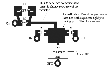
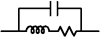
Nevertheless, you need to do something. Most manufacturers of clock sources recommend a circuit somewhat like the one in Figure 12.60, often without the resistor. Using the values and parasitic assumptions listed in Table 12.5 and the layout in Figure 12.60, this filter achieves better than to 20 dB of power supply noise reduction in the frequency band from 10 MHz to 1 GHz (10 9 Hz). Cascading two sections roughly doubles the attenuation. The purpose of the resistor is to preclude resonance at the frequency f C where the filter begins to function. That frequency f C , called the low-pass cutoff, is given by
Equation 12.19
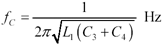
Figure 12.60. This filter provides reasonable attenuation of power supply noise from 10 MHz to 1000 MHz.
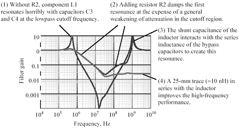
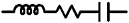
Without the resistor R1 installed, the cutoff-frequency resonance appears in Figure 12.61 at a frequency of 500 KHz. A reasonable value of R 1 that provides the right amount of damping to prevent such a resonance at f C is
Equation 12.20
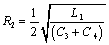
Figure 12.61. The frequency response of a realistic filter is an amalgamation of compromises.
With this resistance installed, the loss slope of the filter is “20 dB per decade. One decade above f C you can expect an attenuation of roughly 20 dB.
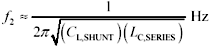
Above 100 MHz the parasitic shunt capacitance of the inductor ( C L,SHUNT ) begins to short out the inductor. At the same frequency the parasitic series inductance of the capacitor ( L C,SERIES ) substantially degrades its performance. This is a general example of the principle that at high frequencies, components do the opposite of what you want (inductors turn into capacitors and vice versa). At 1 GHz the parasitic effects render the filter totally ineffective .
The frequency at which a one-stage filter becomes totally degraded depends on the values of the parasitic elements. It is usually somewhere in the vicinity of this value:
Equation 12.21
|
where |
C L,SHUNT is the parasitic shunt capacitance of the inductor, F, and |
|
L C,SERIES is the parasitic series inductance of the network of capacitors, H. |
For the component values listed in Table 12.5 this resonance should appear at 1 GHz. As expected, a debilitating resonance appears at that frequency in Figure 12.61. The solution to this problem is to include a short trace on the downstream side of inductor L 1 . Provided the trace is laid out with its input and output well separated, it exhibits almost no end-to-end shunt capacitance. This trick increases the series impedance of the overall L 1 structure, disrupting the parasitic resonance at 1 GHz.
Table 12.5. Parasitic Models for Components in Power Filter
|
Resistance |
Inductance |
Capacitance |
Circuit model |
|
|
L 1 |
.1 |
1 uH |
100 pF |
|
|
R 2 |
2.2 |
1 nH |
1 pF |
|
|
C 3 , C 4 |
.1 |
0.5 nH |
.047 uF |
|

Filters designed for wideband operation are built as a cascade of multiple sections, each section scaled to provide coverage in successively higher frequency bands, which is what has been done here. Before you attempt any type of advanced filter design, it is crucial that you measure and understand the parasitic parameters of your components. For inductors, the main parasitic elements are a shunt capacitance and a series resistance; for capacitors the main parasitic elements are a series inductance and a series resistance. These values are an integral part of any filter you build and must be included in your calculations.
When laying out any high-frequency filter, take care to keep the input and output well separated. All capacitors should preferably connect directly to a solid reference plane with large vias, at least 500 m m (20 mil) diameter. Keep all extraneous circuit traces as short as possible (less than 2.5 mm, or 0.1 in.), unless included intentionally as part of the circuit. Surface-mounted components, in the smallest size practicable, work best.
POINT TO REMEMBER
- Filters designed for wideband operation are built from a cascade of multiple sections, each section scaled to provide coverage in successively higher frequency bands.
12.12.1 Healthy Power
POINT TO REMEMBER
- Observing the noise between V CC and ground always returns useful information.
12.12.2 Clean Power
POINT TO REMEMBER
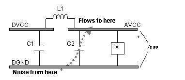
- A power-supply filter does not eliminate noise ”it merely copies junk from one circuit node to another, eliminating the difference between them.
Fundamentals
- Impedance of Linear, Time-Invariant, Lumped-Element Circuits
- Power Ratios
- Rules of Scaling
- The Concept of Resonance
- Extra for Experts: Maximal Linear System Response to a Digital Input
Transmission Line Parameters
- Transmission Line Parameters
- Telegraphers Equations
- Derivation of Telegraphers Equations
- Ideal Transmission Line
- DC Resistance
- DC Conductance
- Skin Effect
- Skin-Effect Inductance
- Modeling Internal Impedance
- Concentric-Ring Skin-Effect Model
- Proximity Effect
- Surface Roughness
- Dielectric Effects
- Impedance in Series with the Return Path
- Slow-Wave Mode On-Chip
Performance Regions
- Performance Regions
- Signal Propagation Model
- Hierarchy of Regions
- Necessary Mathematics: Input Impedance and Transfer Function
- Lumped-Element Region
- RC Region
- LC Region (Constant-Loss Region)
- Skin-Effect Region
- Dielectric Loss Region
- Waveguide Dispersion Region
- Summary of Breakpoints Between Regions
- Equivalence Principle for Transmission Media
- Scaling Copper Transmission Media
- Scaling Multimode Fiber-Optic Cables
- Linear Equalization: Long Backplane Trace Example
- Adaptive Equalization: Accelerant Networks Transceiver
Frequency-Domain Modeling
- Frequency-Domain Modeling
- Going Nonlinear
- Approximations to the Fourier Transform
- Discrete Time Mapping
- Other Limitations of the FFT
- Normalizing the Output of an FFT Routine
- Useful Fourier Transform-Pairs
- Effect of Inadequate Sampling Rate
- Implementation of Frequency-Domain Simulation
- Embellishments
- Checking the Output of Your FFT Routine
Pcb (printed-circuit board) Traces
- Pcb (printed-circuit board) Traces
- Pcb Signal Propagation
- Limits to Attainable Distance
- Pcb Noise and Interference
- Pcb Connectors
- Modeling Vias
- The Future of On-Chip Interconnections
Differential Signaling
- Differential Signaling
- Single-Ended Circuits
- Two-Wire Circuits
- Differential Signaling
- Differential and Common-Mode Voltages and Currents
- Differential and Common-Mode Velocity
- Common-Mode Balance
- Common-Mode Range
- Differential to Common-Mode Conversion
- Differential Impedance
- Pcb Configurations
- Pcb Applications
- Intercabinet Applications
- LVDS Signaling
Generic Building-Cabling Standards
- Generic Building-Cabling Standards
- Generic Cabling Architecture
- SNR Budgeting
- Glossary of Cabling Terms
- Preferred Cable Combinations
- FAQ: Building-Cabling Practices
- Crossover Wiring
- Plenum-Rated Cables
- Laying Cables in an Uncooled Attic Space
- FAQ: Older Cable Types
100-Ohm Balanced Twisted-Pair Cabling
- 100-Ohm Balanced Twisted-Pair Cabling
- UTP Signal Propagation
- UTP Transmission Example: 10BASE-T
- UTP Noise and Interference
- UTP Connectors
- Issues with Screening
- Category-3 UTP at Elevated Temperature
150-Ohm STP-A Cabling
- 150-Ohm STP-A Cabling
- 150- W STP-A Signal Propagation
- 150- W STP-A Noise and Interference
- 150- W STP-A: Skew
- 150- W STP-A: Radiation and Safety
- 150- W STP-A: Comparison with UTP
- 150- W STP-A Connectors
Coaxial Cabling
- Coaxial Cabling
- Coaxial Signal Propagation
- Coaxial Cable Noise and Interference
- Coaxial Cable Connectors
Fiber-Optic Cabling
- Fiber-Optic Cabling
- Making Glass Fiber
- Finished Core Specifications
- Cabling the Fiber
- Wavelengths of Operation
- Multimode Glass Fiber-Optic Cabling
- Single-Mode Fiber-Optic Cabling
Clock Distribution
- Clock Distribution
- Extra Fries, Please
- Arithmetic of Clock Skew
- Clock Repeaters
- Stripline vs. Microstrip Delay
- Importance of Terminating Clock Lines
- Effect of Clock Receiver Thresholds
- Effect of Split Termination
- Intentional Delay Adjustments
- Driving Multiple Loads with Source Termination
- Daisy-Chain Clock Distribution
- The Jitters
- Power Supply Filtering for Clock Sources, Repeaters, and PLL Circuits
- Intentional Clock Modulation
- Reduced-Voltage Signaling
- Controlling Crosstalk on Clock Lines
- Reducing Emissions
Time-Domain Simulation Tools and Methods
- Ringing in a New Era
- Signal Integrity Simulation Process
- The Underlying Simulation Engine
- IBIS (I/O Buffer Information Specification)
- IBIS: History and Future Direction
- IBIS: Issues with Interpolation
- IBIS: Issues with SSO Noise
- Nature of EMC Work
- Power and Ground Resonance
Points to Remember
Appendix A. Building a Signal Integrity Department
Appendix B. Calculation of Loss Slope
Appendix C. Two-Port Analysis
- Appendix C. Two-Port Analysis
- Simple Cases Involving Transmission Lines
- Fully Configured Transmission Line
- Complicated Configurations
Appendix D. Accuracy of Pi Model
Appendix E. erf( )
Notes
EAN: N/A
Pages: 163
