RC Region
Near DC the magnitude of the inductive reactance of a transmission line w L dwindles to insignificance in comparison to its DC resistance. All that matters below this point is the relation between the DC resistance of the line and its capacitance (Section 3.2).
In more technical terms, the RC, or dispersive , region includes all combinations of w and l for which the line behaves in a distributed manner but for which the frequency remains sufficiently low that the magnitude of the per-unit-length series inductance ( w L ) fails to rise to any significance compared to the per-unit-length DC resistance ( R DC ). In this lowest -frequency distributed region both attenuation and phase shift depend solely on the transmission line's DC resistance and capacitance.
A transmission line operated in this region is termed an RC transmission line , or sometimes a dispersive transmission line . The partial differential equations describing the behavior of such a line are called diffusion equations , and the line is sometimes called a diffusion line . The term diffusion line is popular with physicists and mechanical engineers .
POINT TO REMEMBER
- The terms RC transmission line, dispersive transmission line, and diffusion line all mean the same thing.
3.5.1 Boundary of RC Region
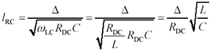
As illustrated in Figure 3.2, the RC region extends from DC up to freqeuncy w LC . At this frequency the reactive component of the propagation coefficient ( w L ) equals in magnitude the resistive component ( R DC ).
Equation 3.53

|
where |
w LC is the upper limit of the RC region, rad/s, |
|
R DC is the series DC resistance of the transmission line (signal and return resistances added together), W /m, |
|
|
L is the series inductance, H/m. |
|
|
NOTE: |
For differential configurations define R DC as the sum of the resistances of the outbound and returning conductors, and L as the inductance of the differential transmission line thus formed , L = Z DIFFERENTIAL / v DIFFERENTIAL . |
If at the maximum length and maximum anticipated operating frequency your transmission line satisfies conditions [3.24] and [3.25], then you may bypass any consideration of the peculiar properties of the RC region and use instead a lumped-element approximation (i.e., the pi model) to determine how your system will respond.
Let's look for a moment at the confluence of [3.24] and [3.53] as illustrated in Figure 3.2. The exact length at the intersection of these two constraints is found by substituting the LC mode cutoff frequency [3.53] into constraint [3.24]. This calculation reveals a critical length l RC below which you need never concern yourself with the distributed RC mode of operation.
Equation 3.54
|
where |
l RC represents the critical length below which distributed RC behavior never appears, m, |
|
D is an arbitrary constant customarily set to 1/4, |
|
|
R DC is the series DC resistance of the transmission line (signal and return resistances added together), W /m, |
|
|
L is the series inductance, H/m, and |
|
|
C is the shunt capacitance, F/m. |
Equation [3.54] tells you that the distributed RC mode of operation matters only at lengths sufficiently great that the total DC resistance of the line lR DC becomes noticeable compared to the high-frequency value of impedance  . For example, in Figure 3.2 a horizontal line drawn at the 1-m level passes from the lumped-element mode directly into the LC mode, skipping the distributed-RC mode altogether. This happens because a 1/2-oz, 50- W pcb trace with a width of 150 microns (6 mils) and a length of 1 m has a DC resistance of only 6.3 W , much less than the line impedance of 50 W . Such a line will never exhibit any observable RC-mode phenomenon . Designers of pcbs therefore needn't concern themselves with the RC mode of behavior.
Conversely, a much longer pcb trace of the same type, perhaps 100 m in length, would exhibit the signs of distributed RC operation over the band from a few kilohertz to several megahertz .
The critical length defined in [3.54] varies dramatically with the size of the conductors. If a given cross section is scaled by a factor of k in all dimensions, the L and C parameters remain unchanged, but the resistance changes inversely with the square of k . This quadratic change in resistance precipitates a change in l RC by a factor of k 2 .
Larger conductors, such as 24-gauge telephone wire, will not exhibit observable RC behavior until you reach lengths on the order of 100 meters . Smaller conductors, such as found within integrated circuits, may exhibit observable RC behavior at lengths much shorter than the dimensions of the chip package. The RC effect within integrated circuits is exacerbated by the low conductivity of some materials (like polysilicon) used to construct the transmission structures.
POINTS TO REMEMBER
- The RC region extends in frequency from DC up to that point w LC where the magnitude of the line inductance ( w LC L ) equals the DC resistance ( R DC ).
- For any transmission line there exists a critical length below which you need never concern yourself with the distributed RC mode of operation.
3.5.2 Input Impedance (RC Region)
In general the input impedance [3.16] of a transmission structure varies strongly with the length of the line and the type of load connected. This can at times be a distinct disadvantage , particularly when you wish to equalize the propagation function of a transmission line by using a reactive source or load impedance.
For example, if the input impedance of a transmission structure Z IN were known, you could design a suitable reactive source-impedance network Z S such that the propagation function Z IN /( Z IN + Z S ) achieved some arbitrary equalization goal. Unfortunately, variations in Z IN with line length and loading complicate the design of a good equalizer (see [3.16]).
There are, however, some special cases under which the problem can be simplified. These cases share a common principle of controlling (or ignoring) reflections.
The first case has already been mentioned in Section 2.2.1, "Definition of Characteristic Impedance Z C ." It happens during that brief interval of time after your driver has generated its first rising edge but before the first reflection arrives from the far end. During this brief interval the input impedance of the line equals precisely Z C independent of the line length. A source-end equalizer designed to work into an impedance of Z C would for a brief time operate properly until the moment the first reflection arrived, after which the performance of the equalizer would change.
The second case happens when you eliminate reflections by providing an end-termination load Z L . The end-termination impedance must be adjusted such that Z L = Z C . Once the termination is in place, the input impedance of the structure equals precisely Z C independent of line length. You should verify this fact using [3.16]. A source- equalizing network Z S may then be designed such that the propagation function Z C /( Z C + Z S ) achieves your equalization goal.
In the third case, a source-termination network with an impedance Z S equal to Z C may be used. This network provides a driving-point impedance at the load that does not vary with line length. In this case the end-termination impedance Z L must be calculated so that Z L /( Z L + Z C ) achieves your equalization goal.
The fourth method assumes a very long transmission line, sufficiently long that the transfer gain H falls to significantly less than one. Under this assumption, the inverse-gain H “1 vastly exceeds H , so much so that the term H may be neglected in equation [3.16]. Suitable rearrangement of the terms in [3.16] shows that under this assumption Z IN equals Z C .
POINTS TO REMEMBER
- The input impedance of a line without reflections is predictable and independent of line length.
- An RC transmission line may be equalized using a suitable reactive source or load impedance network.
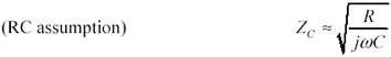
3.5.3 Characteristic Impedance (RC Region)
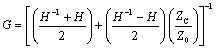
The full expression for characteristic impedance ( neglecting the conductance G ) includes contributions from both the inductance L and resistance R of the line.
Equation 3.55

Taking advantage of the defining assumption of the RC mode, namely that the term w L remains small compared to R , the characteristic impedance in the heart of the RC territory may be approximated.
Equation 3.56
Expression [3.56] is a complex function of frequency with a phase angle of “45 ° and a magnitude slope of -10 dB per decade .
Depending on the frequency regime in which you choose to operate a line, it behaves either as an RC transmission line (at low frequencies) or a low-loss transmission line (at high frequencies). These cases are distinguished by the relative magnitudes of the inductive and resistive impedances in [3.55]: At frequencies below w LC the characteristic impedance varies as given by [3.56]. Above w LC the characteristic impedance may be derived from [3.55] under the assumption that w L vastly exceeds R , leading to the conclusion that at high frequencies the characteristic impedance asymptotically approaches a constant value of  .
.
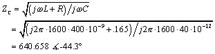
Example of an RC Transmission Line
You probably have RC transmission lines in your house. The two wires running from the nearest central telephone switching office to your phone are usually AWG-24 wire. These wires are twisted in a configuration yielding the following line parameters:
Equation 3.57
At 1600 Hz (the center of the voice band), the characteristic impedance of this configuration is
Equation 3.58
This calculation explains the myth that telephone wires have a characteristic impedance of roughly 600 ohms. That's the correct impedance in the voice band, but at high frequencies the characteristic impedance Z is 100 ohms.
Note that the characteristic impedance in the RC region varies markedly with frequency. Designing a good-quality termination for operation in the RC region is not a trivial project. For best operation, the termination must match Z C over the entire frequency range spanned from w LE and w LC . The difficulty of designing a network to match Z C over this range (i.e., the number of poles required in the network) is proportional to the number of octaves of frequency spanned.
Fortunately, good terminations for RC structures become necessary only if you are constructing a hybrid circuit for two-way communication (see Section 8.3.3, "UTP: Hybrid Circuits") or an equalizer. For general-purpose one-way communication, an RC structure may be left open -circuited at the far end, relying on the natural damping effect of the series resistance to quell reflections.
POINT TO REMEMBER
- Within the RC region, characteristic impedance is a complex function of frequency with a phase angle of “45 ° and a magnitude slope of -10 dB per decade.
3.5.4 General Behavior within RC Region
Figure 3.8 illustrates the propagation function of a unit- sized RC transmission line ( R = 1 W /m, C = 1F/m, and l = 1m). The response is given under three conditions of loading. In all three cases the line is driven with a low-impedance voltage source. The solid curve shows the propagation function with the end open-circuited. This curve displays the least overall loss at high frequencies. It represents the most often-used configuration for general digital connections made on-chip using transmission structures operated in the RC mode.
Figure 3.8. A matching end terminator on an RC transmission line produces a sloping transfer function.
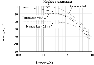
The dashed curve shows what happens to the transfer gain of your transmission line (dashed line) when you apply a perfectly matched end-termination impedance equal at frequencies to Z C ( w ). The matched end termination degrades the line response in two ways: It reduces the available signal at the far end of the line, and it introduces a disagreeable tilt to the propagation function. Of the two problems, the tilt in the propagation function is the more serious, because it will introduce significant amounts of intersymbol interference. Sufficiently large intersymbol interference causes bit errors.
Binary signaling tolerates a tilt of no more than about 3 dB (and certainly never more than 6 dB) in the channel attenuation over the band occupied by the coded data. Any tilt greater than that amount must be flattened out with an equalizer (see Section 3.14, "Linear Equalization: Long Backplane Trace Example").
In summary, the only good reasons for using a matched end termination with an RC transmission line are
- As part of a hybrid circuit (see Section 8.3.3, "UTP: Hybrid Circuits").
- To stabilize the input impedance of the channel as part of an equalization circuit.
The dotted curves in Figure 3.8 correspond to two different values of resistive loads, equal to 1/2 or 1/10 respectively of the aggregate series resistance of the transmission line. In both cases the purely resistive load reduces the level of the output signal, but while flattening the overall attenuation curve instead of making it worse , as with the matched termination. The flattened attenuation curve, whose flat zone now reaches to a higher frequency than previously, makes possible simple binary signaling at a higher bandwidth than would have been possible with an open-circuited (or end- terminated ) RC transmission line.
The resistive load establishes a classic gain-bandwidth tradeoff whereby you can improve the bandwidth of your channel at the expense of reducing the signal amplitude. The upper limit to which the bandwidth may be pushed is established by the onset of the LC mode of operation, which takes precedence at that point where the inductance of the line becomes significant in comparison to the series resistance. Because the proper value for a resistive end termination in the LC mode equals the high-frequency value of characteristic impedance,  , you will see numerous examples of lines designed for operation in the crossover zone between RC and LC modes using a purely resistive end termination equal to Z . This value has the property of eliminating reflections at very high frequencies within the LC band while also providing a relatively flat propagation function within the RC band. This is the circuit most often used in digital telephone circuits operating at a few tens or hundreds of kilobits/s over twisted-pair cabling at distances up to approximately 1 km.
POINTS TO REMEMBER
- A perfectly-matched end termination applied to an RC transmission line renders the input impedance of the structure indepedant of line length. This advantage comes at the expense of a terrible degradation of the transfer response.
- A fixed resistance at the end of an RC transmission line flattens the gain curve, providing more usable bandwidth at the expense of a reduction in the received signal amplitude, and a greater variation with line length in the input impedance of the structure.
- A purely resistive end termination equal to
 eliminates reflections within the LC band while also providing a relatively flat propagation function within the RC band.
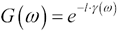
3.5.5 Propagation Coefficient (RC Region)
The transfer equations for the RC mode are derived beginning with [3.13] and [3.14], neglecting the contribution of the line inductance parameter L , and also neglecting variations in R and C that generally occur only at higher frequencies.
Equation 3.59

Equation 3.60

3.5.6 Transfer Function (RC Region)
Substitute expression [3.60] into [3.17] along with appropriate assumptions about the source and load impedances to calculate the overall propagation function.
3.5.6.1 Propagation Function of RC Line with Open-Circuited Load
From [3.17], assuming Z S = 0 and Z L =  ,
,
Equation 3.61
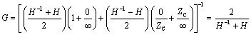
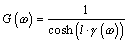
Substituting [3.14] for H, the formula for G may be reduced using a hyperbolic cosine:
Equation 3.62
|
where |
G is the propagation function of the transmission-line circuit composed of a voltage source, RC transmission line, and open-circuited load, |
|
the hyperbolic cosine function cosh( x ) = ( e x + e “x )/2, |
|
|
l is the line length, m, |
|
|
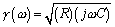
the transmission line propagation coefficient |
|
|
R and C are the values of resistance and capacitance, in units of W /m and F/m, respectively. |
 , and
, and3.5.6.2 Propagation Function of RC Line with Matched End Termination
From [3.17], assuming ZS = 0 and ZL = ZC,
Equation 3.63
Substituting [3.14] for H, the formula for G may be evaluated:
Equation 3.64
|
where |
G is the propagation function of the transmission-line circuit composed of a voltage source, RC transmission line, and perfectly matched load, |
|
l is the line length, m, |
|
|
The transmission line propagation coefficient |
|
|
R and C are the values of resistance and capacitance, in units of W /m and F/m, respectively. |
3.5.6.3 Propagation Function of RC Line with Matched Source Termination
From [3.17], assuming ZS = ZC and ZL = ,
Equation 3.65
This arrangement gives the same result as [3.63].
3.5.6.4 Propagation Function of RC Line with Resistive End Termination
From [3.17], assuming ZS = 0 and ZL = Z0, the high-frequency value of characteristic impedance.
Equation 3.66
Equation 3.67
Equation [3.67] admits little in the way of further simplification. If you are considering a resistive termination of value Z0 for a line of length l that crosses between the RC and LC modes, you can calculate from DC analysis a value for G (0) = Z /( Z + lR DC ), while the LC mode gain is given approximately by equation [3.95] 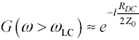 . The difference between these two values defines a minimum perturbation in the propagation function of your circuit between the DC and LC modes.
If the transfer response is not suitably flat using a resistive end termination, try applying resistive terminations to both ends of the line. Although this technique does not produce a perfect response, it cuts by about half the percentage variation in gain between DC and LC modes at the expense of a reduction by by half in the received signal amplitude.
POINT TO REMEMBER
- A resistive termination at both ends of an RC-LC mixed-mode transmission line provides flatter gain than termination at only one end or the other.
3.5.7 Normalized Step Response (RC Region)
Figure 3.9 illustrates the step response of the same unit-sized RC transmission line used in the previous section ( R = 1 W /m, C = 1F/m, and l = 1m).
Figure 3.9. On an RC transmission line a resistive termination produces the fastest but smallest step edge.
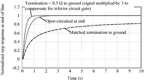
The solid curve shows the propagation function with the end open-circuited. It represents the most often-used configuration for general digital connections made on-chip using transmission structures operated in the RC mode.
The dashed curve shows the degraded risetime that occurs when you apply a perfectly matched end-termination impedance equal to Z C ( w ).
The dotted curve illustrates the superior risetime achievable with a resistive termination at the cost of a reduced signal amplitude. In this case the DC gain of the circuit is 1/3, so the signal in the graph has been multiplied by three so you can easily compare the 10% to 90% risetime of the result against the other two signals.
Table 3.4 presents the normalized step response of an RC transmission line under selected conditions of loading. You may scale the values in this table to fit your transmission structure by multiplying all the time values listed in the table by the factor RCl 2 , where R and C represent the resistance and capacitance per unit length of your transmission structure in units of W /m and F/m respectively, and l is its length in meters.
Table 3.4. Normalized Step Response of RC Transmission Line
|
Percentile (of step height) |
End-termination condition |
|||
|---|---|---|---|---|
|
Open |
Matched |
Z L = ( lR) /2 (gain = 1/3) |
Z L = ( lR) /10 (gain = 1/11) |
|
|
10% |
0.105 |
0.185 |
0.069 |
0.053 |
|
20% |
0.160 |
0.304 |
0.101 |
0.073 |
|
50% |
0.354 |
1.099 |
0.198 |
0.139 |
|
80% |
0.726 |
7.790 |
0.376 |
0.252 |
|
90% |
1.006 |
31.664 |
0.507 |
0.338 |
|
NOTE ”All times are expressed in seconds. |
||||
POINT TO REMEMBER
- A fixed resistance at the end of an RC transmission line improves the settling time at the expense of a reduction in the received signal amplitude.
3.5.8 Tradeoffs Between Distance and Speed (RC Region)
The scaling equation associated with Table 3.4 indicates that the risetime scales with the square of length. Thus, the speed of operation achievable within the RC region scales inversely with the square of transmission-line length. For example, given a fixed receiver architecture and assuming the bit error rate (BER) of the receiver is dominated by errors due to intersymbol interference, a 10% increase in length increases the line attenuation by 10%. To regain a normal signal amplitude at the end of a transmission line operated in the RC mode, the 10% increase in attenuation must be offset by a 20% reduction in the system operating speed.
POINT TO REMEMBER
- The speed of operation achievable within the RC region scales inversely with the square of transmission-line length.
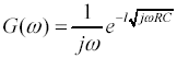
3.5.9 Closed-Form Solution for Step Response (RC Region)
An analytic solution for the step response of an RC transmission line is known for only one configuration of loading. Unfortunately, this solution corresponds to the least popular configuration: a line with a matched end termination. The step response for other configurations is best derived using the full system-modeling equations given in Chapter 4.
The derivation begins with equation [3.64], which presents the propagation function (impulse response) of an RC line with a perfectly matched end termination. Multiplying that result by the Fourier-transform operator 1/ j w produces the step response G :
Equation 3.68
Define a constant  :
:
Equation 3.69
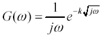
The inverse Fourier transform of this entity is known:
Equation 3.70
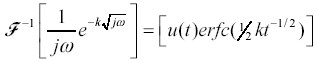
Reinserting the value of k produces the step response g * as a function of time.
Equation 3.71
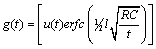
3.5.10 Elmore Delay Estimation (RC Region)
W. C. Elmore in 1948 published a marvelous way to estimate the delay of RC circuits [30] . Adaptations of his original method are used today as the primary means of validating on-chip timing.
The Elmore delay-estimation method applies to well-damped circuits composed of any number of series resistances and shunt capacitances. It does not apply (in its original form) to circuits involving inductance, resonance , overshoot, or any form of poorly damped or nonmonotonic behavior.
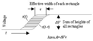
The simple one-stage RC low-pass filter in Figure 3.10 illustrates the general principle involved, which is that there exists some effective width t for the shaded region such that the area A of the shaded region equals the step voltage D V multiplied times t . The variable t is defined
Equation 3.72
Figure 3.10. The area of the shaded region equals the step height D V multiplied by the effective width t .
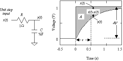
Elmore asserts that under a wide range of conditions the 50% input-to-output delay of the circuit approximately equals t . For example, if the output waveform had a linear slope, the relation t 50% = t would hold exactly.
The Elmore delay-estimation procedure first determines the area A , and then computes t using [3.72]. The determination of A hinges on the observation that whenever node x ( t ) steps through a voltage range D V the total charge on capacitor C changes by an amount D Q equal to C D V . Furthermore, this exact amount of charge D Q must have passed through resistor R .
The passage of charge D Q through resistor R causes a momentary voltage difference between the ends of the resistor:
Equation 3.73
|
where |
i ( t ) is the current waveform necessary to charge the capacitor. |
By definition the total integrated current i ( t ) equals D Q , the step change in charge:
Equation 3.74
Substituting equation [3.73] for i ( t ) in [3.74],
Equation 3.75
The integral term equals the area A of the shaded region divided by R:
Equation 3.76

Rearranging the terms and recognizing D Q =C D V ,
Equation 3.77

Equation [3.77] suggests that the total integrated area A between curves x ( t ) and y ( t ) is a function only of the step change in voltage D V , the resistance R , and the amount of capacitance C downstream of R . It is not a function of the exact shape of the rising edge, the speed of the driver, or any other factors.
Substituting A = t D V from [3.72] into the left side of [3.77] produces the Elmore delay equation, which relates the effective width of the shaded region t to both R and C .
Equation 3.78

Equation 3.79

The final step in the process assumes the 50% input-to-output delay of the circuit approximately equals the effective width of the shaded region, t .
The Elmore estimate, crude as it may be, is surprisingly effective. It is exact in cases where the output waveform is monotonic and a strictly delayed version of the input waveform. To prove this exactness I must prove that for y ( t ) = x ( t “ t ) the area A between x and y equals t D V . Such a case is illustrated in Figure 3.11, where the area A is broken into a set of rectangles of equal height and width whose total area clearly equals t D V .
Figure 3.11. The total area contained between waveforms x ( t ) and x ( t “ t ) scales linearly with t .
When the input risetime significantly exceeds the response time of the circuit (that is, t is much less than t 10 “90% ), the output waveform tends to look like a strict delay of the input waveform and the Elmore delay becomes exact.
When the input risetime equals or falls short of the response time of the circuit, the output waveform becomes distorted and the Elmore delay serves only as an estimate of delay. For well-damped RC circuits with monotonic inputs, the Elmore delay t always over estimates the actual circuit delay.
Figure 3.12 illustrates the step response of an RC low-pass filter showing the Elmore delay estimate and the actual 50% delay. The Elmore estimate of delay is t = RC = 1. At that point in time the actual step response has ascended to 63.2% of its final value. The 50%-point delay for the step response of a one-stage RC low-pass filter occurs at 0.69 t .
Figure 3.12. The effective delay of an RC circuit roughly equals the product RC .
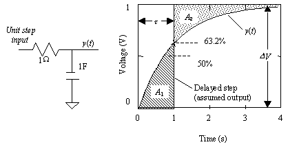
The Elmore delay t by definition exists at that point in time that equalizes the areas A 1 and A 2 marked on Figure 3.12. Step-response waveforms having symmetrical precursor and postcursor waveforms tend to attain 50% amplitude precisely as indicated by the Elmore delay estimate. Step-response waveforms that have a mostly concave-down shape tend to attain 50% amplitude sooner than indicated by the Elmore delay estimate.
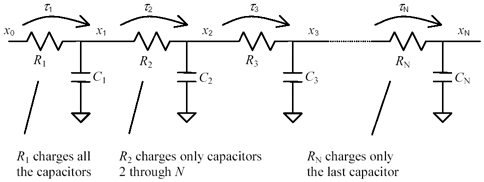
When composing networks of multiple RC sections, the Elmore principle still applies, but its application becomes slightly more complicated. Figure 3.13 depicts a multi-element configuration. The resistor R 1 in this figure charges all N capacitors downstream of its own position. The Elmore estimated delay t 1 from point x to x 1 is therefore  . Resistor R 2 charges only capacitors numbered 2 through N , so the estimated delay from point x 1 to x 2 is
  . Working down row, the total delay for the whole circuit is estimated:
Equation 3.80
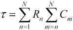
Figure 3.13. Each resistor charges successively less capacitance.
The special case of a very large number of stages representing a continuous transmission line operated in the RC dispersion region lends itself to some simplifications . In this case we will assume the line has a total series resistance of R and a total parasitic capacitance to the reference plane of C . The line is driven by a low-impedance source on the left and unterminated at the far end. An N -element circuit model for this configuration would look like Figure 3.13 with all the resistances set to R / N and all the capacitances set to C / N .
Observe that in the N -element model the first resistor charges the full line capacitance C , while the last resistor in the chain charges almost nothing. In general the average capacitance charged by any resistor along the structure equals C/2. The average estimated delay at each stage is therefore ( R / N )( C /2), and the total delay for N such stages must equal ½ RC . This is the Elmore delay estimate for an unterminated transmission line operated in the RC dispersion region when driven by a low-impedance source.
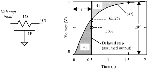
Figure 3.14 illustrates the step response of a continuous dispersive RC transmission line, computed using the FFT method (see Chapter 4). The symbol for a dispersive transmission line is a resistor with a line under it representing the distributed capacitance to the nearest reference plane. The transmission line in Figure 3.14 has a total series resistance of 1 W and a total shunt capacitance of 1F. It is driven by a low impedance at one end and is open-circuited at the other. The Elmore estimate of delay is t = ½ RC = ½ sec. At that point in time the actual step response has ascended to 65.2% of its final value. The 50%-point delay for the step response of an unloaded RC transmission line occurs at 0.71 t . Chip designers often assume the delay of an RC transmission line is 0.35 RC , which comes from the formula 0.71(1/2) RC .
Figure 3.14. The Elmore delay estimate for a distributed RC transmission line equals ½ RC .
Elmore delay calculations for a continuous RC dispersion-limited transmission line coincide with delay calculations for the C-R-C "pi" network indicated in Figure 3.14. The pi network is a very reasonable lumped-element approximation for a short RC dispersion-limited transmission line, where short means the Elmore delay is a small fraction of the signal risetime.
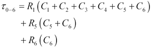
To apply the Elmore delay concept to a tree-structured circuit, you must identify all the resistors R i that lie along a path from the input to the output under analysis. Then, for each series resistor R i you must identify the total downstream capacitance C i charged by that resistance and sum all the R i C i time constants. For the schematic in Figure 3.15 the path from input to x 4 traverses resistors R 1 , R 2 , R 3 , and R 4 . The Elmore delay estimate for this path is
Equation 3.81
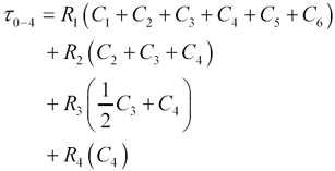
Figure 3.15. The Elmore algorithm quickly computes a reasonable upper bound for the delay of complicated tree and bus structures.
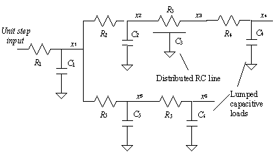
Resistors R 5 and R 6 are not involved in this calculation, but capacitors C 5 and C 6 are involved.
In the calculation of t 0-4 note that resistor R 3 effectively feeds only half the distributed capacitance of the RC transmission line, whereas resistors R 2 and R 1 , being upstream of the distributed element must feed the entire distributed capacitance C 3 .
The Elmore estimate from input to x 6 is
Equation 3.82
The appeal of the Elmore delay-estimating algorithm is its ability to quickly compute a reasonable upper bound on the delay of complicated tree and bus structures used on-chip. SPICE could of course be used to find a more accurate estimate, but the computational complexity of SPICE precludes its use for day-to-day on-chip floor-planning purposes.
In practice, the Elmore delay estimate may be successfully applied to well-damped RC networks, but not for transmission lines having appreciable amounts of inductance or for nonmonotonic inputs. Ismail [31] has worked out a promising approach that extends the Elmore delay-estimation algorithm to account for transmission line inductance.
POINTS TO REMEMBER
- The Elmore delay approximation takes into account only the resistance and capacitance of a transmission configuration. It applies to well-damped circuits composed of any number of series resistances, shunt capacitances, and distributed RC transmission lines.
- The Elmore delay approximation does not apply circuits involving inductance, resonance, overshoot, or any form of poorly damped or nonmonotonic behavior.
- The Elmore delay for a lumped resistance R feeding a total downstream capacitance of C is RC .
- The Elmore delay for a distributed RC transmission line having total resistance R and distributed capacitance C is (1/2) RC .
Fundamentals
- Impedance of Linear, Time-Invariant, Lumped-Element Circuits
- Power Ratios
- Rules of Scaling
- The Concept of Resonance
- Extra for Experts: Maximal Linear System Response to a Digital Input
Transmission Line Parameters
- Transmission Line Parameters
- Telegraphers Equations
- Derivation of Telegraphers Equations
- Ideal Transmission Line
- DC Resistance
- DC Conductance
- Skin Effect
- Skin-Effect Inductance
- Modeling Internal Impedance
- Concentric-Ring Skin-Effect Model
- Proximity Effect
- Surface Roughness
- Dielectric Effects
- Impedance in Series with the Return Path
- Slow-Wave Mode On-Chip
Performance Regions
- Performance Regions
- Signal Propagation Model
- Hierarchy of Regions
- Necessary Mathematics: Input Impedance and Transfer Function
- Lumped-Element Region
- RC Region
- LC Region (Constant-Loss Region)
- Skin-Effect Region
- Dielectric Loss Region
- Waveguide Dispersion Region
- Summary of Breakpoints Between Regions
- Equivalence Principle for Transmission Media
- Scaling Copper Transmission Media
- Scaling Multimode Fiber-Optic Cables
- Linear Equalization: Long Backplane Trace Example
- Adaptive Equalization: Accelerant Networks Transceiver
Frequency-Domain Modeling
- Frequency-Domain Modeling
- Going Nonlinear
- Approximations to the Fourier Transform
- Discrete Time Mapping
- Other Limitations of the FFT
- Normalizing the Output of an FFT Routine
- Useful Fourier Transform-Pairs
- Effect of Inadequate Sampling Rate
- Implementation of Frequency-Domain Simulation
- Embellishments
- Checking the Output of Your FFT Routine
Pcb (printed-circuit board) Traces
- Pcb (printed-circuit board) Traces
- Pcb Signal Propagation
- Limits to Attainable Distance
- Pcb Noise and Interference
- Pcb Connectors
- Modeling Vias
- The Future of On-Chip Interconnections
Differential Signaling
- Differential Signaling
- Single-Ended Circuits
- Two-Wire Circuits
- Differential Signaling
- Differential and Common-Mode Voltages and Currents
- Differential and Common-Mode Velocity
- Common-Mode Balance
- Common-Mode Range
- Differential to Common-Mode Conversion
- Differential Impedance
- Pcb Configurations
- Pcb Applications
- Intercabinet Applications
- LVDS Signaling
Generic Building-Cabling Standards
- Generic Building-Cabling Standards
- Generic Cabling Architecture
- SNR Budgeting
- Glossary of Cabling Terms
- Preferred Cable Combinations
- FAQ: Building-Cabling Practices
- Crossover Wiring
- Plenum-Rated Cables
- Laying Cables in an Uncooled Attic Space
- FAQ: Older Cable Types
100-Ohm Balanced Twisted-Pair Cabling
- 100-Ohm Balanced Twisted-Pair Cabling
- UTP Signal Propagation
- UTP Transmission Example: 10BASE-T
- UTP Noise and Interference
- UTP Connectors
- Issues with Screening
- Category-3 UTP at Elevated Temperature
150-Ohm STP-A Cabling
- 150-Ohm STP-A Cabling
- 150- W STP-A Signal Propagation
- 150- W STP-A Noise and Interference
- 150- W STP-A: Skew
- 150- W STP-A: Radiation and Safety
- 150- W STP-A: Comparison with UTP
- 150- W STP-A Connectors
Coaxial Cabling
- Coaxial Cabling
- Coaxial Signal Propagation
- Coaxial Cable Noise and Interference
- Coaxial Cable Connectors
Fiber-Optic Cabling
- Fiber-Optic Cabling
- Making Glass Fiber
- Finished Core Specifications
- Cabling the Fiber
- Wavelengths of Operation
- Multimode Glass Fiber-Optic Cabling
- Single-Mode Fiber-Optic Cabling
Clock Distribution
- Clock Distribution
- Extra Fries, Please
- Arithmetic of Clock Skew
- Clock Repeaters
- Stripline vs. Microstrip Delay
- Importance of Terminating Clock Lines
- Effect of Clock Receiver Thresholds
- Effect of Split Termination
- Intentional Delay Adjustments
- Driving Multiple Loads with Source Termination
- Daisy-Chain Clock Distribution
- The Jitters
- Power Supply Filtering for Clock Sources, Repeaters, and PLL Circuits
- Intentional Clock Modulation
- Reduced-Voltage Signaling
- Controlling Crosstalk on Clock Lines
- Reducing Emissions
Time-Domain Simulation Tools and Methods
- Ringing in a New Era
- Signal Integrity Simulation Process
- The Underlying Simulation Engine
- IBIS (I/O Buffer Information Specification)
- IBIS: History and Future Direction
- IBIS: Issues with Interpolation
- IBIS: Issues with SSO Noise
- Nature of EMC Work
- Power and Ground Resonance
Points to Remember
Appendix A. Building a Signal Integrity Department
Appendix B. Calculation of Loss Slope
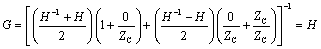
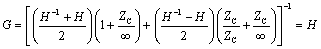
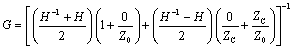
Appendix C. Two-Port Analysis
- Appendix C. Two-Port Analysis
- Simple Cases Involving Transmission Lines
- Fully Configured Transmission Line
- Complicated Configurations
Appendix D. Accuracy of Pi Model
Appendix E. erf( )
Notes
EAN: N/A
Pages: 163
