Dielectric Loss Region
Dielectric losses are present at all frequencies, growing progressively more severe at higher frequencies. These losses become noticeable only when they rise to a level comparable with the resistive losses, a point after which the line is said to operate in the dielectric-loss-limited region (Section 3.2).
3.8.1 Boundary of Dielectric-Loss-Limited Region
For typical transmission media used in macroscopic digital applications (i.e., not on-chip), the frequency w d falls low enough that the losses due to dielectric absorption at that frequency are swamped by skin-effect losses. As the frequency is increased, however, the skin-effect loss grows only in proportion to the square root of frequency, while the dielectric loss grows at a faster rate in direct proportion to frequency. Above some frequency w q the dielectric loss equals, and then exceeds, the skin-effect loss.
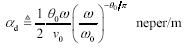
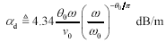
The derivation of w q begins with simple approximations for the skin effect a r and dielectric loss a d , in units of nepers per meter.
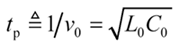
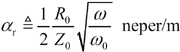 see equation [3.114]
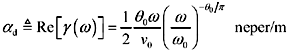
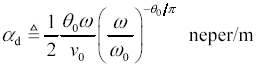 see equation [3.131]
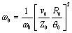
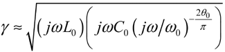
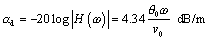
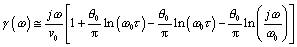
Equating the preceding two expressions while neglecting the slowly varying term ( w / w ) - q / p generates the following formula for the crossover frequency w q .
Equation 3.123
|
where |
w q is the frequency beyond which dielectric losses exceed skin effect losses, rad/s, |
|
w is any arbitrary frequency at which the AC resistance may be specified, rad/s, |
|
|
v is the velocity of propagation at w , m/s, |
|
|
Z is the characteristic impedance of the transmission line at w , W , |
|
|
R is the series AC resistance at w , W /m, and |
|
|
tan q is the loss tangent of the dielectric material at frequency w . |
|
|
NOTE: |
For differential configurations, define R to represent the sum of the AC resistances of both outbound and returning conductors, and Z as the impedance of the differential transmission line thus formed . |
In coaxial and twisted-pair transmission lines constructed from modern, low-loss dielectric materials the dielectric absorption at frequencies below 1 GHz accounts for only a small portion of the overall loss, but at some point in the range 1 to 10 GHz it can become quite significant. Radiation losses from such conducting structures, while very important to the radiated emissions problem, are generally so tiny that for signal integrity purposes they may also be ignored.
In the pcb realm dielectric losses can emerge as a significant problem at frequencies below 1 GHz due to the use of poor dielectric materials (like FR-4).
Beware the width of the mixing zone between the skin-effect and dielectric-effect regions . It is extremely broad, because the relative difference between skin effect and dielectric losses (in dB/m) changes only as fast as the square root of frequency, and also because the effects add directly "in phase." At a frequency 10 times lower than w q , skin-effect losses exceed dielectric losses by only a factor of  . The dielectric loss at this frequency contributes fully 24% of the overall attenuation. At a frequency 10 times higher than w q , the situation reverses. The dielectric loss at this frequency contributes 76% of the overall attenuation. Assuming the transmission performance is dominated by only resistive (i.e., skin-effect) and dielectric losses, Table 3.8 lists the percentage of total signal loss contributed by each factor.
The distinguishing feature of the dielectric-loss region is that within this region the characteristic impedance remains fairly flat, while the line attenuation in dB varies in direct proportion to frequency.
POINT TO REMEMBER
- Skin-effect loss grows only in proportion to the square root of frequency, while the dielectric loss grows in direct proportion to frequency. Above some frequency w q the dielectric loss equals, and then exceeds, the skin-effect loss.
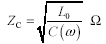
3.8.2 Characteristic Impedance (Dielectric-Loss-Limited Region)
The full expression for characteristic impedance (neglecting the conductance G ) includes contributions from the external inductance L , resistance R , and capacitance of a transmission line.
Equation 3.124
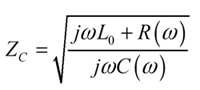
In the limit as you proceed to frequencies far above w LC , the contribution of the term R becomes negligible, leading to this approximation for characteristic impedance at any frequency above the skin-effect onset.
Equation 3.125
The only difference between this and the previous equation [3.85] is that here I explicitly provide for the possibility that the resistance R ( w ) and capacitance C ( w ) may each change with frequency, and the inductance term is clearly marked L to represent only the external inductance of the transmission configuration (see Section 2.7, "Skin-Effect Inductance" and Section 2.8, "Modeling Internal Impedance"). External inductance is the value of series inductance, in Henries per meter, computed by a two-dimensional field solver under the assumption that current rides on the surface of each conductor without penetrating its bodies.
Table 3.8. Relative Skin and Dielectric Losses
|
Relative operating frequency: w / w q (rad/s) |
Percentage of loss contributed by skin effect |
Percentage of loss contributed by dielectric effect |
Loss slope [1] |
|---|---|---|---|
|
.0001 |
99 |
1 |
.505 |
|
.001 |
97 |
3 |
.515 |
|
.01 |
91 |
9 |
.545 |
|
.1 |
76 |
24 |
.62 |
|
1 |
50 |
50 |
.75 |
|
10 |
24 |
76 |
.88 |
|
100 |
9 |
91 |
.955 |
|
1000 |
3 |
97 |
.985 |
|
10000 |
1 |
99 |
.995 |
[1] NOTE (1) ”The loss slope is defined as the slope of a curve showing the log of dB attenuation along the vertical axis and the log of frequency along the horizontal, as in Figure 3.1. A loss slope of a indicates the transmission loss in dB is growing proportional to f a at that frequency (see Appendix B).
The lumped-element , RC, and LC operating analyses presented previously assume that both L and R are constants, so it is therefore not generally necessary in those presentations to distinguish between the internal and external inductance, only lumping together all the inductance you have of either type under the umbrella term "L." Here the term  from Equation [3.5] is used to represent the external inductance L e . The internal inductance of the signal conductors is represented by variations in the imaginary part of R ( w ).
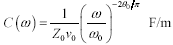
The capacitance model [3.7] expresses the dielectric properties of the insulating medium surrounding your conductors as a single complex-valued function C ( w ). The real part of C ( w ), when multiplied by the operating frequency j w , represents displacement current flowing within the insulator. The total displacement current (in unit of A/m) is proportional to j w Re( C ( w )) V , where V is the voltage impressed upon the transmission line at any one point. The displacement current flows in quadrature with the applied electric field. The displacement current effect acts like what you normally think of as capacitance.
The imaginary part of C ( w ), when multiplied by the operating frequency j w , generates a conduction current that flows in phase with the applied voltage. It is a peculiar coincidence that the magnitude of conduction current in the sorts of insulators used for high-speed digital applications happens to vary in almost direct proportion to frequency ”that's what makes it reasonable to approximate the conduction current using a model like j w ( j · Im( C ( w ))) V . Those persons accustomed to seeing a conductance parameter G in the transmission equations will recognize that the term j w ( j · Im( C ( w ))) plays the role of G in [3.124] and [3.125]. Because the imaginary part of C ( w ) from [3.7] is always negative, the term j w ( j · Im( C ( w ))), representing the conductance in S/m, is positive.
As your operating frequency crosses upward from the skin-effect region to the dielectric region, the variations in C ( w ) change (slightly) the precise shapes of the asymptotically convergent curves in Figure 3.17, but not the asymptotic points of convergence (Figure 3.27). As long as your circuit does not depend on the precise shapes of the curves, the changes are of little practical significance.
If the precise shape of the impedance curve is of importance to your design (for example, in the construction of ultra -accurate terminations it would be crucial), then you should know that the skin-effect losses and dielectric losses have opposite effects on the shape of the characteristic impedance curve.
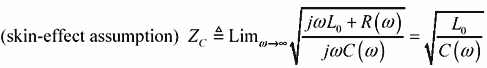
The plots starting with Figure 3.32 and going through Figure 3.35 all depict a hypothetical pcb trace having a fixed DC resistance of 6.4 W /m plus the skin effect, and with a dielectric loss tangent of 0.025. The trace is a 50-ohm stripline constructed of 1/2-oz copper (17.4 micron thickness ) on FR-4 with a width of 150 microns (6 mils, v = 1.446 ·10 8 m/s, L = 346 nH/m, C = 138 pF/m). The trace is 0.5 meters long.
Figure 3.32. In the vicinity of the skin-effect onset, skin-effect and dielectric losses affect the characteristic impedance in opposite directions.
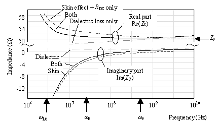
Figure 3.32 illustrates the relative influence of skin effect and dielectric losses on the characteristic impedance of a lossy line. The chart depicts the characteristic impedance of a trace with only skin-effect and DC resistive losses (assuming a perfect dielectric), a trace with only dielectric losses (assuming zero resistance), and a combination of both.
The topmost three curves in each case show the real part of impedance, and the bottom three curves, the imaginary part. Compared to a base case that includes no losses of any type, skin-effect losses increase the real part of the impedance curve in the vicinity of the skin-effect onset at w d , while the dielectric losses decrease the impedance in the same area. The two effects almost cancel each other in the band near w d , causing the characteristic impedance in this region to approach the asymptotic value marked Z more rapidly and more completely than when either effect is present alone. The cancellation is nothing more than a grand coincidence. Do not depend on the cancellation effect to stabilize the impedance of a practical design, as the values of dielectric loss in most materials vary substantially with temperature and water content.
At frequencies above the onset of the dielectric-loss-limited mode w q , dielectric losses ultimately force the characteristic impedance back up above Z . This happens because of the slow deterioration in line capacitance with increasing frequency caused by the dielectric loss.
The general relationship between the characteristic impedance and input impedance is given by [3.33] and discussed in Section 3.5.2 "Input Impedance (RC Region)" and in Section 3.2.1 "A Transmission Line Is Always a Transmission Line."
POINTS TO REMEMBER
- In the vicinity of the skin-effect onset w d the skin effect increases characteristic impedance while dielectric loss decreases it.
- At frequencies above the onset of the dielectric-loss-limited mode w q , dielectric losses ultimately force the characteristic impedance back up above Z .
3.8.3 Influence of Dielectric Loss on TDR Measurement
Dielectric losses progressively diminish the available line capacitance as you move to higher and higher frequencies, thereby causing an upward tilt to a plot of characteristic impedance versus frequency. In the time domain, the tilt suggests that the effective impedance measured over very short scales of time should exceed that measured at larger scales of time. Figure 3.33 illustrates precisely that effect.
Figure 3.33. The dielectric effect starts with a higher impedance and then trends lower, while the resistive effects do the opposite.
The detailed blow-up of the first plateau in the TDR response for a lossy transmission line shows three waveforms: the response of a trace with only skin-effect and DC resistance losses (assuming a perfect dielectric), a trace with only dielectric losses (assuming zero resistance), and a combination of both.
The dielectric losses produce a negative slope in the first plateau. The resistive losses create a positive slope. Working together, the two effects almost cancel, in this particular example, creating a slope less steep than when either effect is present alone ”the same peculiar coincidence mentioned in the previous section. It cannot be depended upon to stabilize the impedance of a practical design, as the values of dielectric loss in most materials vary substantially with temperature and water content.
Dielectric loss distorts the slope in the first plateau, obliterating your ability to accurately infer the resistance of the line from a single TDR plot.
For any open -circuited transmission line, [30] the second plateau of the TDR response shows a signal which has traversed the line twice, going to the far end and then reflecting back. This reflected signal displays the marks of its round-trip venture in the form of a noticeable dispersion of both rising and falling edges.
[30] The usual condition of measurement for checking the impedance of a pcb test coupon .
POINT TO REMEMBER
- Dielectric losses cause an upward tilt to a plot of characteristic impedance versus frequency. Resistive losses create a neagtive slope. Working together, the two effects can sometimes almost cancel, creating a TDR slope less steep than when either effect is present alone.
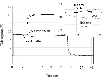
3.8.4 Propagation Coefficient (Dielectric-Loss-Limited Region)
Figure 3.34 shows the propagation coefficient for the same hypothetical pcb trace as Figure 3.32, but this time in addition showing dielectric and skin effect loss. This figure plots the real and imaginary parts of the propagation coefficient versus frequency. The plot is drawn with log-log axes to highlight the polynomial relationships between portions of the curves.
Figure 3.34. Below w q the resistive losses dominate. Above w q the dielectric losses matter most.
In the RC region below w LC both the real part of the propagation coefficient (log of attenuation) and the imaginary part (phase in radians) rise together in proportion to the square root of frequency. Above w LC the imaginary part (phase) grows linearly with increasing frequency, while the real part (attenuation) inflects to the right at a lesser slope. The dotted line extending horizontally to the right illustrates the effect on the real part of the propagation coefficient of DC resistance alone. The DC resistance produces a loss coefficient that is constant with frequency. Combining the DC resistance with skin-effect losses produces the dashed line marked "With skin effect."
The chart splits out the real and imaginary parts of the dielectric effect separately, showing them as dashed lines with a slope of +1. These curves represent the phase and magnitude coefficients that would accrue to a hypothetical transmission line with dielectric losses only, but no resistance. Comparing the dashed line for pure dielectric loss (marked "Dielectric loss") with the dashed line representing pure resistive losses (marked "With skin effect"), you can see that below the frequency marked w q the losses are dominated by resistive effects, and above w q by dielectric effects.
In the skin-effect region the overall line attenuation (solid line marked "Re( g )") grows proportional to the square root of frequency. In the absence of dielectric losses the attenuation would continue with the same slope forever. Once dielectric losses enter the picture, however, the slope becomes steeper. Above the point w q where the dielectric losses take effect the attenuation grows in direct proportion to frequency.
In this example all the regions are crammed fairly close together with the result that the attenuation curve does not show explicit regions with perfect slopes. Instead, it describes a smooth arc with graduated changes in slope between regions.
In the dielectric region the decoupling of phase and attenuation is less complete than in the LC and skin-effect regions. Above w q the ratio of phase (radians) to attenuation (nepers) never exceeds 2/ q , limiting the maximum Q of any resonator you might try to build. Because microwave designers like to make high-Q circuits, this limitation renders high-loss materials, like FR-4, practically useless for their applications. Digital designers, on the other hand, who strive to build low-Q, nonresonant circuits, discover that FR-4 is a very useful material even up to frequencies as high as 10-GHz, provided that their traces are kept sufficiently short that the line attenuation does not become a problem.
Terminations are used within the dielectric region to abate resonance on long transmission lines in precisely the same manner as used in LC regions.
You can predict the phase and amplitude response of a dielectric-loss-limited transmission line beginning with the definition of the propagation function [3.13]. To make this calculation, you must assume operation at a frequency so far in excess of w q that the dielectric losses dominate the performance of the circuit so that the resistive (skin-effect and DC) losses may be safely ignored. In practice such a situation is created when a large, fat conductor is combined with a high-loss dielectric material. For example, a microstrip trace 5000 microns wide (200 mils), as might be used in a microwave application to mitigate skin-effect loss, if implemented on an FR-4 substrate, would enter the dielectric region at a frequency just below 10 MHz. The propagation coefficient above 1 GHz would be 91% dominated by the dielectric effect.
Rewriting [3.13] to ignore the resistive effects, and substituting [3.7] [31] for the capacitive term,
[31] This equation makes the assumption that the loss tangent is constant with frequency.
Equation 3.126
Group the ordinary inductive and capacitive terms, substitute  , and remember to divide the exponent (2 q / p ) by two as it is pulled out from under the radical .
Equation 3.127
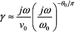
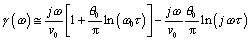
Next isolate the exponential j term.
Equation 3.128
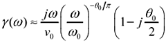
Assuming q to be a small positive constant, you may represent the term ( j ) - q / p by a linear expression. For q less than 0.1 the error in this approximation is less than one part in 800.
Equation 3.129
The imaginary portion of [3.129] is a linear-phase term very nearly equal to j w /v . This term represents the bulk transport delay of the transmission-line medium. The real portion of [3.129] is the same but a factor of q /2 smaller. It represents a low-pass filter whose attenuation in dB grows in direct proportion to frequency. [32]
[32] Remember that the real part of the propagation coefficient shows the attenuation in nepers. Increasing attenuation at high frequencies indicates a decreasing , or low-pass filtering, propagation function H (see [3.14]).
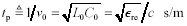
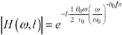
The linear-phase term implies that the one-way propagation function H of a dielectric-loss-limited transmission line, for frequencies above w q , acts primarily as a large time-delay element. The bulk propagation delay in units of seconds per meter for frequencies near w is given by
Equation 3.130
Equation [3.130] may also be stated in terms of the effective relative permittivity  re associated with the transmission-line configuration
 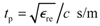 , assuming the speed of light c = 2.998 ·10 8 m/s and further assuming the relative magnetic permeability m r equals one (see [2.28]).
The bulk transport delay varies in proportion to the length of the transmission line and slightly with frequency (see Section 3.8.6, "Step Response (Dielectric-Loss-Limited Region)"). Doubling the length doubles the bulk transport delay.
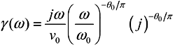
The transfer loss in nepers per meter is given by the real part of the propagation function. This value is called the dielectric loss coefficient :
Equation 3.131
If you are operating in a fairly narrow band near w , you may omit from your calculation the term ( w / w ) - q / p without much loss of accuracy. This is the standard practice for RF designers, who then convert the attenuation in nepers to dB, leading to this expression for the attenuation per meter:
Equation 3.132
The low-pass filtering action of the dielectric-loss effect implies that the step response will be dispersed, slurring crisp rising edges into edges of limited rise and fall time, according to the properties of the filter.
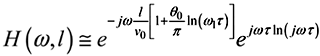
The magnitude of H is determined from the real part of the propagation function (see [2.16]):
Equation 3.133
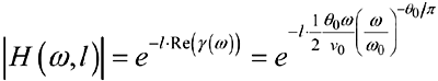
|
where |
H ( w ,l ) is the magnitude of the low-pass filter function implied by [3.129], |
|
l is the length of the transmission line in meters, |
|
|
w is the frequency at which AC line parameters are specified, rad/s, |
|
|
v is the velocity of propagation at frequency w , m/s, and |
|
|
tan q is loss tangent of the dielectric material at frequency w . |
The signal loss represented by H , measured in nepers (or decibels), varies in proportional to the length of the transmission line and in proportion to the square root of frequency. Double the distance yields twice the loss in neper or decibel units (one neper equals 8.6858896 dB). Doubling the frequency multiplies the loss (in neper or dB units) by two.
Binary signaling tolerates a tilt of no more than about 3 dB (and certainly never more than 6 dB) in the channel attenuation over the band occupied by the coded data. Any tilt greater than that amount must be flattened out with an equalizer (see Section 3.14, "Linear Equalization: Long Backplane Trace Example"). Be careful with your units conversions when calculating attenuation, as the data rate f for most systems is expressed in Hertz, while the frequency argument for the function H ( w ) is specified in radians per second. You must multiply f by 2 p to get w .
The properties in Table 3.9 hold only for dielectric-limited transmission lines operated at frequencies well above w q and for which the dielectric loss tangent remains constant with frequency.
POINTS TO REMEMBER
- The attenuation (in dB) within the dielectric-loss-limited region grows in direct proportion to frequency.
- Doubling the length of a dielectric-loss-limited transmission line doubles the attenuation.
Table 3.9. Summary of Dielectric-Limited Transmission Line Properties at Frequencies Well Above w q
|
Property |
Formula |
Ref. equation |
|---|---|---|
|
Asymptotic value of characteristic impedance |
|
[3.125] |
|
Bulk transport delay per meter (for frequencies near w ) |
|
[3.130] |
|
Attenuation in nepers per meter. NOTE: For use only over a narrow range of frequencies, you may omit the term ( w / w ) - q / p . |
|
[3.131] |
|
Attenuation in decibels per meter. (1 neper = 8.6858896 decibels) NOTE: For use only over a narrow range of frequencies, you may omit the term ( w / w ) - q / p . |
|
[3.132] |
|
Transfer gain at length l |
|
[3.133] |
|
Inductance per meter |
|
[3.5] |
|
Capacitance per meter (varies slightly with frequency) |
|
[3.7] |

3.8.5 Possibility of Severe Resonance within Dielectric-Loss Limited Region
Transmission lines operated in the dielectric region fall prey to the same resonance difficulties that afflict structures operated in the LC-region. The termination means used to conquer resonance are the same as those described in Section 3.6.6, "Terminating an LC Transmission Line."
Dielectric losses have the beneficial effect of reducing (somewhat) the requirements for efficacy of intentional terminations placed in a circuit, in the same way as skin-effect losses (see Section 3.7.5, "Possibility of Severe Resonance within Skin-Effect Region"), with the exception that in the dielectric region the heights of the resonant peaks of the transfer gain (measured in dB) fall off inversely with frequency.
3.8.5.1 Subtle Differences Between Termination Styles
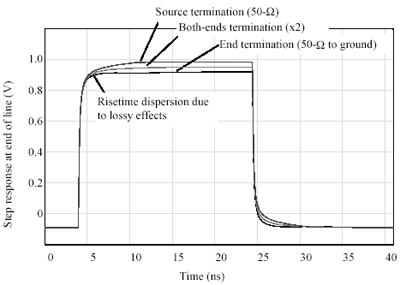
Figure 3.25 is repeated here as Figure 3.35, this time showing the inclusion of skin-effect losses. All three traces clearly show dispersion of the rising and falling edges caused by the low-pass filtering properties of the skin-effect resistance. In comparison to the results in Figure 3.30, the source- and end-terminated circuits shown here benefit from a partial cancellation of the corrective terms applied to the characteristic impedance function by the resistive and dielectric loss effects respectively. The both-ends terminated circuit provides the best performance, independent of any requirement for balance between the resistive and dielectric loss mechanisms.
Figure 3.35. The source- and end-terminated circuits shown here benefit from a partial cancellation of the corrective terms applied to the characteristic impedance function by the resistive and dielectric loss effects respectively.
3.8.5.2 Application of Termination Equations to Other Regions
Although the LC, skin-effect, and dielectric-loss-limited regions all share the same asymptotic high-frequency parameter for characteristic impedance Z , the dielectric effect induces a gradual rise in the actual characteristic impedance Z C in proportion to the log of freqeuncy. This gradual rise suggests that the best value of termination for a dielectric-loss-limited structure is probably  , where C ( w ) is calculated near your anticipated maximum frequency of operation.
The same general termination approaches therefore work in all three regions, delivering in each case an overall circuit gain G nearly equal to the one-way propagation function H applicable within each region.
POINTS TO REMEMBER
- The dielectric effect induces a gradual rise in the characteristic impedance Z C in proportion to the log of freqeuncy.
- Transmission lines in the dielectric-loss-limited region fall prey to the same resonance difficulties that afflict the LC region and respond to the same means of termination.
3.8.6 Step Response (Dielectric-Loss-Limited Region)
This section presents the step response of a dielectric-effect-limited transmission line. The applicability of these results hinges on two crucial assumptions:
- The risetime of the step input to the system must be substantially faster than the dielectric-effect risetime, meaning that the shape of the output waveform is determined primarily by the system itself and not strongly influenced by the precise risetime of the input step, and
- The dielectric losses greatly exceed the resistive losses so that you have a true dielectric-limited transmission media and not a resistively limited media.
The solution requires knowledge of these parameters:
- tan q , the loss tangent of the dielectric material at frequency w ,
- v , the velocity of propagation at frequency w , m/s,
- l , the length of the line (m), and
- w , some particular frequency at which the high-frequency line parameters are specified (rad/s).
The derivation of step response begins with [3.127], into which you may substitute the following infinite series. [33]
[33] Burnigton, Handbook of Mathematical Table and Formulas , Handbook Publishers, Inc., 3rd ed., 1948, p 44.
Equation 3.134
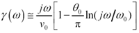
Making the identifications a = j w / w and x = - q / p produces this expression for the propagation coefficient [3.127]:
Equation 3.135
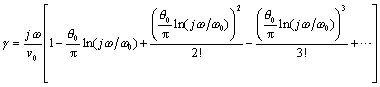
In cases where the constant ( q / p ) is much smaller than unity and w lies within a reasonable factor of w you may safely ignore all but the first two terms of the substitution.
Equation 3.136
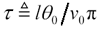
The next step both adds and subtracts a peculiar logarithmic term inside the square brackets: ( q / p )ln( w t ). The purpose of this operation is to mold the equation into a separable form so that the fixed bulk delay may be isolated from a canonical low-pass filter function. The constant t is defined
Equation 3.137
The new version of [3.136] with the peculiar terms added and subtracted is
Equation 3.138
Combine the arguments of the right-most two logarithmic terms, and then distribute the term j w /v into the result.
Equation 3.139
Multiply [3.139] by the (negative of the) transmission line length l and exponentiate (as in [3.14]) to find H .
Equation 3.140
The first exponential term in [3.140] represents a linear-phase bulk transport delay. The amount of delay ( l/v )[1 + ( q / p )ln( w t )] depends not only on the nominal line delay l/v but also on the dielectric loss and other variables . This delay, for the purposes of investigating attenuation and dispersion of the propagated signals, may be ignored. The second component e j w t ln( j w t ) represents a frequency-varying low-pass filter that accounts for the peculiar shape of the dielectric loss step response.
To compute the step response of the dielectric effect, multiply [3.140] by 1/ j w and then apply an inverse Fourier transform. Multiplying by 1/ j w converts [3.140] from an impulse-response to a step-response. Evaluating the inverse Fourier transform of the result produces a time-domain waveform representing the step response g ( t ) associated with the dielectric effect.
Equation 3.141
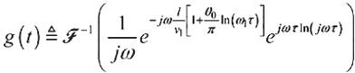
There is no recognized closed-form expression for this inverse Fourier transformation. It is best evaluated by sampling [3.141] on a dense grid of frequencies and using an inverse FFT to determine the step response.
Figure 3.36 compares the magnitude of the propagation function (in dB) of a long, perfectly terminated skin-effect-limited channel with that of a perfectly dielectric loss-limited channel. The “3 dB points on the two curves are very close. The bottom part of the figure compares the step responses of the two channels. The skin-effect step response displays a sharper initial rise due to the larger magnitude of its high-frequency content, but a longer, more slowly-evolving tail due to the unusual behavior of its frequency response near DC.
Figure 3.36. As a function of time, the dielectric step response begins more slowly than the skin-effect response, but finishes sooner.
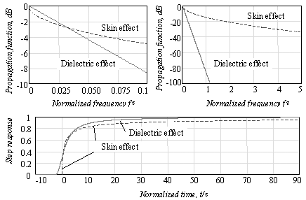
The normalized dielectric-loss step response g 1 ( t ) in Figure 3.36 is derived from [3.141] by ignoring the fixed bulk delay and then setting t = 1.
Equation 3.142
From the normalized step response g 1 ( t ) you may determine the complete step response g ( t ) by first scaling the time axis by a factor of t and then delaying by amount ( l/v )[1 + ( q / p )ln( w t )].
Equation 3.143
Assuming you know the value t defined in [3.137], you may read directly from Figure 3.36 the frequency response (magnitude) and step response (assuming a normalized 1-volt step input with zero risetime) for any dielectric-effect limited system.
As impressive as this chart may appear, please do not make the mistake of assuming it accurately predicts real-world dielectric effects. The skin effect has a precise physical model and behaves in a very predictable way, but the dielectric approximations discussed here depend for their accuracy on the assumption of constant dielectric loss across a very wide band. Although this may be the form of the specification for many materials, if you look at the actual dielectric loss curves, you will find the loss is not constant, but undulates slowly between inflection points, coming near the specification at perhaps more than one location but (hopefully) never crossing it. The charts in Figure 3.36 represent the behavior of a worst-case system with constant dielectric loss set at the maximum value q across all frequencies of interest.
In Figure 3.36 the dielectric step response begins before time zero. This happens because at very high frequencies above w , as the dielectric of the insulating material deteriorates [3.7], the propagation velocity of the transmission line slightly exceeds v . Some portions of your signal therefore arrive just before you might have predicted based upon consideration of v alone. This behavior does not constitute a violation of causality . All that has happened is that the bulk delay subtracted from the normalized step-response curve presented in Figure 3.36 is (apparently) a little too generous. Correcting Figure 3.36 by the amount of delay stipulated in [3.140] places the step-response waveform in the correct position.
Beware that the skin effect and dielectric loss effects mix over a very broad range of frequencies. It's rare in pcb problems that you see dielectric losses without also having to take into account skin-effect dispersion. The best general rule for combining dispersion due to different sources is the sum-of-squares rule, which works as follows .
Equation 3.144
If you seek a more exact answer, use the frequency-domain model defined in Section 3.1, "Signal Propagation Model," sample it on a dense grid of frequencies, and inverse-FFT the result to get a full time-domain step response (see also Chapter 4).
POINT TO REMEMBER
- Given two systems with the same “3dB loss at frequency f 1 , one system having only dielectric losses and the other having only skin-effect losses, the dielectric step response begins more slowly than the skin-effect response, but finishes sooner.
3.8.7 Tradeoffs Between Distance and Speed (Dielectric-Loss Region)
Given a fixed receiver architecture, and assuming the BER of the receiver is dominated by errors due to intersymbol interference, the speed of operation within the dielectric-absorption zone scales inversely with the transmission-line length. This tradeoff between length and speed arises because of the unit slope of the dielectric-absorption attenuation curve. For example, a 10% increase in transmission-line length increases the attenuation (in dB) by 10%. To regain a normal signal amplitude at the end of a transmission line limited by dielectric-absorption, the 10% increase in attenuation must be offset by a 10% reduction in system operating speed.
POINTS TO REMEMBER
- The risetime of a dielectric-loss-limited channel scales directly with its length.
- The speed of operation within the dielectric-loss region scales inversely with transmission-line length.
- A dielectric medium with twice the loss tangent incurs twice the loss (in dB) and induces a settling time twice as long.
- It's rare in pcb problems that you see skin-effect losses without also having to take into account dielectric dispersion.
Fundamentals
- Impedance of Linear, Time-Invariant, Lumped-Element Circuits
- Power Ratios
- Rules of Scaling
- The Concept of Resonance
- Extra for Experts: Maximal Linear System Response to a Digital Input
Transmission Line Parameters
- Transmission Line Parameters
- Telegraphers Equations
- Derivation of Telegraphers Equations
- Ideal Transmission Line
- DC Resistance
- DC Conductance
- Skin Effect
- Skin-Effect Inductance
- Modeling Internal Impedance
- Concentric-Ring Skin-Effect Model
- Proximity Effect
- Surface Roughness
- Dielectric Effects
- Impedance in Series with the Return Path
- Slow-Wave Mode On-Chip
Performance Regions
- Performance Regions
- Signal Propagation Model
- Hierarchy of Regions
- Necessary Mathematics: Input Impedance and Transfer Function
- Lumped-Element Region
- RC Region
- LC Region (Constant-Loss Region)
- Skin-Effect Region
- Dielectric Loss Region
- Waveguide Dispersion Region
- Summary of Breakpoints Between Regions
- Equivalence Principle for Transmission Media
- Scaling Copper Transmission Media
- Scaling Multimode Fiber-Optic Cables
- Linear Equalization: Long Backplane Trace Example
- Adaptive Equalization: Accelerant Networks Transceiver
Frequency-Domain Modeling
- Frequency-Domain Modeling
- Going Nonlinear
- Approximations to the Fourier Transform
- Discrete Time Mapping
- Other Limitations of the FFT
- Normalizing the Output of an FFT Routine
- Useful Fourier Transform-Pairs
- Effect of Inadequate Sampling Rate
- Implementation of Frequency-Domain Simulation
- Embellishments
- Checking the Output of Your FFT Routine
Pcb (printed-circuit board) Traces
- Pcb (printed-circuit board) Traces
- Pcb Signal Propagation
- Limits to Attainable Distance
- Pcb Noise and Interference
- Pcb Connectors
- Modeling Vias
- The Future of On-Chip Interconnections
Differential Signaling
- Differential Signaling
- Single-Ended Circuits
- Two-Wire Circuits
- Differential Signaling
- Differential and Common-Mode Voltages and Currents
- Differential and Common-Mode Velocity
- Common-Mode Balance
- Common-Mode Range
- Differential to Common-Mode Conversion
- Differential Impedance
- Pcb Configurations
- Pcb Applications
- Intercabinet Applications
- LVDS Signaling
Generic Building-Cabling Standards
- Generic Building-Cabling Standards
- Generic Cabling Architecture
- SNR Budgeting
- Glossary of Cabling Terms
- Preferred Cable Combinations
- FAQ: Building-Cabling Practices
- Crossover Wiring
- Plenum-Rated Cables
- Laying Cables in an Uncooled Attic Space
- FAQ: Older Cable Types
100-Ohm Balanced Twisted-Pair Cabling
- 100-Ohm Balanced Twisted-Pair Cabling
- UTP Signal Propagation
- UTP Transmission Example: 10BASE-T
- UTP Noise and Interference
- UTP Connectors
- Issues with Screening
- Category-3 UTP at Elevated Temperature
150-Ohm STP-A Cabling
- 150-Ohm STP-A Cabling
- 150- W STP-A Signal Propagation
- 150- W STP-A Noise and Interference
- 150- W STP-A: Skew
- 150- W STP-A: Radiation and Safety
- 150- W STP-A: Comparison with UTP
- 150- W STP-A Connectors
Coaxial Cabling
- Coaxial Cabling
- Coaxial Signal Propagation
- Coaxial Cable Noise and Interference
- Coaxial Cable Connectors
Fiber-Optic Cabling
- Fiber-Optic Cabling
- Making Glass Fiber
- Finished Core Specifications
- Cabling the Fiber
- Wavelengths of Operation
- Multimode Glass Fiber-Optic Cabling
- Single-Mode Fiber-Optic Cabling
Clock Distribution
- Clock Distribution
- Extra Fries, Please
- Arithmetic of Clock Skew
- Clock Repeaters
- Stripline vs. Microstrip Delay
- Importance of Terminating Clock Lines
- Effect of Clock Receiver Thresholds
- Effect of Split Termination
- Intentional Delay Adjustments
- Driving Multiple Loads with Source Termination
- Daisy-Chain Clock Distribution
- The Jitters
- Power Supply Filtering for Clock Sources, Repeaters, and PLL Circuits
- Intentional Clock Modulation
- Reduced-Voltage Signaling
- Controlling Crosstalk on Clock Lines
- Reducing Emissions
Time-Domain Simulation Tools and Methods
- Ringing in a New Era
- Signal Integrity Simulation Process
- The Underlying Simulation Engine
- IBIS (I/O Buffer Information Specification)
- IBIS: History and Future Direction
- IBIS: Issues with Interpolation
- IBIS: Issues with SSO Noise
- Nature of EMC Work
- Power and Ground Resonance
Points to Remember
Appendix A. Building a Signal Integrity Department
Appendix B. Calculation of Loss Slope
Appendix C. Two-Port Analysis
- Appendix C. Two-Port Analysis
- Simple Cases Involving Transmission Lines
- Fully Configured Transmission Line
- Complicated Configurations
Appendix D. Accuracy of Pi Model
Appendix E. erf( )
Notes
EAN: N/A
Pages: 163
