The Jitters
POINT TO REMEMBER
- PLL-based clock generators require a stable, low-jitter reference clock.
12.11.1 When Clock Jitter Matters
Clock jitter comes into play whenever you transfer data between synchronous domains that are controlled by independent clocks. At the boundary between the two domains there will inevitably occur at least one synchronizing register that accepts data from one domain yet is clocked by the other. If the relative clock jitter between the two domains is too great, it will violate the timing margins on the synchronizing register.
12.11.1.1 Clock Jitter Rarely Matters within the Boundaries of a Synchronous State Machine
In a simple, synchronous state machine with only one clock, what matters most is the duration of each individual clock period. An adequate measure of jitter in such a system would be a histogram of the clock intervals. A timing interval analyzer is an appropriate instrument for producing such a histogram. Some oscilloscopes can be configured to produce a clock-interval histogram.
Other than the clock interval being too short (or in machines that use poor digital design practices, being too long), no particular pattern of successive long and short intervals is any more damaging to ordinary synchronous logic than any other pattern.
Such is not the case when considering PLL-based architectures.
12.11.1.2 Clock Jitter Propagation
To understand the effect of jitter on a PLL ( phase-locked loop), you must first understand three general properties shared by all PLL circuits: the tracking range, the filtering range, and the implications of resonance with the PLL feedback control system. To explain these three concepts I'm going to introduce an analogy to an integrating control system with which you are probably already very familiar ”your car (Figure 12.53).
Figure 12.53. The state of each car along the roadway is described by its lateral position y ( t ) and angle of travel.
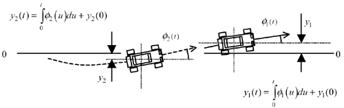
The steering wheel, through a complicated system of linkages and mechanical actions, controls the angle of travel of your vehicle. If you steer straight down the roadway, your lateral position doesn't change. If you steer somewhat to the left and keep moving at the same speed, the car moves linearly to the left (up in the picture) towards increasing values of y . Mathematically speaking, your lateral position y ( t ) along the roadway at any moment is the integral of your direction of travel. If this isn't clear to you, don't worry too much about the mathematics ”all you need to know is that there is a complicated and time-delayed relation between how you handle the wheel and where your car goes. [121]
[121] Those steeped in the art of control system design will recognize that the steering-wheel input determines the rate of change of the angle of travel, so that the entire relation between steering-wheel input and lateral position is that of a double-integral. It is the existence of this double-integration, plus a little bit of delay in your brain, that opens up the possibility of resonance.
Now let's play a high-performance racing game. Imagine you are drafting at 100 mph just inches behind the next driver on a long, straight section of interstate highway . It's your job to follow (track) the movements of the other vehicle as precisely as possible. The other driver is turning his wheel this way and that, trying to throw you off his tail.
If your opponent moves his wheel gradually, you have no difficulty tracking his movements. You see and respond to the graceful movements of his vehicle and have no difficulty following where he's going. This is your tracking behavior.
If your opponent grabs his wheel and violently shakes it, without changing the overall average direction of his vehicle, it makes almost no difference to your strategy. His car may vibrate terribly, but as long as you follow his average direction, you'll still probably be close enough to draft effectively. This is your filtering behavior. You don't even try to duplicate the shaking motion, you just filter it out.
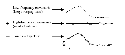
Figure 12.54 decomposes your opponent's trajectory into its high- and low-frequency components. You track the low-frequency part of his motions . These are the long, slow sweeping turns. You ignore his high-frequency behavior (the rapid shaking).
Figure 12.54. A complete trajectory is decomposed into a combination of low-frequency and high-frequency movements.
Let's chart the frequency response of your steering system. To do this, have your opponent first begin moving his vehicle back and forth across the road in a slow, undulating motion y 1 ( t ) = a 1 sin ( w t ). Record the frequency w of his undulations, the amplitude a 1 of his undulations, and the amplitude a 2 of your response. As your opponent slowly increases his rate of undulation from slow to very, very rapid, make a chart showing the system gain a 2 / a 1 versus frequency.
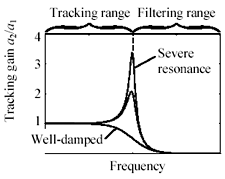
At frequencies within your tracking range, you expect the amplitudes to match perfectly , so the gain is flat (unity gain) in this area. At frequencies within your filtering range, the gain should descend rapidly to zero, because in that area you don't respond. The interesting part happens at the boundary between these two ranges. Most drivers, as the lead car's undulations approach some critical rate, develop acute difficulties. Their response may lag significantly the motions of the lead car, and in their anxious attempts to make up for this delay they will overshoot the mark at the apogee of each excursion. As a result, the frequency-response chart exhibits a gain greater than unity at some particular frequencies. Severe overshoot appears as a large resonant peak in the frequency-response diagram. A system lacking any resonant peak is said to be well-damped .
A mild resonance at the tracking boundary can in some cases help minimize the average tracking error. The practice of causing a mild resonance at the crossover frequency is called PLL peaking . A peaking feature would be a good thing if yours is the only car in the experiment, but any sort of resonance, even a tiny one, spells disaster for a highly cascaded system.
For example, imagine a long chain of N cars drafting each other on the highway. Suppose the first car commences gyrations having a peak-to-peak amplitude of 1 cm precisely at the resonant frequency. If the overshoot of each car at resonance amounts to 10% (a gain of 1.1 at resonance), the gyrating amplitude of car number 2 will be 1.1, car number three will be 1.21, and so on until at car N the gyrating amplitude will be 1.1 N . Fifty cars down the line the peak-to-peak amplitude works out to 117 cm (if they don't careen off the road).
Chaining PLL circuits exponentially exacerbates the effect of resonance. A PLL designed for a chained application must be well damped (no resonance) at all frequencies.
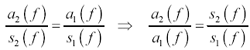
In this analogy please note that you can measure the system gain either by looking at the ratio of amplitudes of the lateral positions of the cars or alternately by looking at the ratio of amplitudes of the steering-wheel inputs. Both measurements return precisely the same frequency-response graph. This works (for identical vehicles) assuming that for each car i , at each frequency, the relation between steering input s i and lateral response a i is the same.
Equation 12.9
|
where |
a 1 and a 2 are the amplitudes of the lateral position undulations of cars 1 and 2 respectively, and |
|
s 1 and s 2 are the amplitudes of the steering-wheel inputs required in cars 1 and 2 respectively to attain the lateral-position amplitudes a 1 and a 2 . |
This principle of similarity extends to measurements made of any matching quantities within the steering control system: steering-wheel inputs, hydraulic-fluid pressures, tie-rod displacements, wheel angles, vehicle angles of travel, or vehicle lateral positions on the roadway. In a PLL the chart of tracking gain versus frequency is called the jitter transfer function.
Before I start to sound too much like Click and Clack, the Tappet brothers, [122] I'd better tie this analogy back to PLL design. Figures 12.55 and 12.56 illustrate the analogous relation between steering systems and clock recovery systems. In Figure 12.55 the angle of travel controls the lateral position of the car with an integrating action. Your eyes compare the position of the lead car with your own, and your brain determines how to best steer the vehicle.
[122] A car-repair radio show popular in the United States.
Figure 12.55. The racing game is described as a linear system.
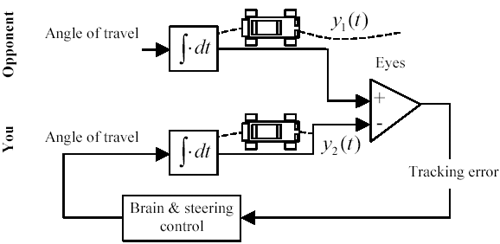
Figure 12.56. A PLL may be described as a linear system.
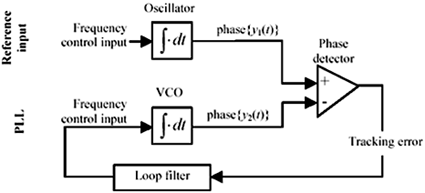
Figure 12.56 illustrates the analogous control system used in a simple frequency-tracking PLL. In this case it is the relative phase of the two input signals that the PLL is designed to control. In the top half of the diagram, the relation between the frequency of oscillation and the phase is shown as an integral. This is derived from the equation for the oscillator, y ( t ) = a sin w t , where if the frequency input w is held constant, the phase w t grows linearly without bound. This type of integrating relation holds between the frequency control input and the output phase of any VCO.
A PLL exhibits many characteristics similar to the highway racing game. It has a tracking range and a filtering range. At the boundary between the two ranges, the PLL control loop may resonate.
What's confusing about PLL terminology is that the main variable of interest is itself a frequency (the reference oscillator frequency), so when analyzing the circuit you have to contemplate the frequency of the variations in the reference oscillator frequency. In physical terms, if you imagine the reference input being FM-modulated, any FM-modulation waveform that occurs at a frequency below the tracking bandwidth is tracked, provided you don't exceed the maximum slew rate specification for the PLL.
The maximum slew rate is the maximum permitted rate of change of the VCO frequency. It is limited by the physical implementation of the VCO circuit, loop filter, and phase detector.
FM-modulation of the reference input at any frequency above the tracking bandwidth is filtered out. High-frequency modulation, because it occurs in the reference signal but not in the reconstituted VCO output, comprises a source of phase error. In a digital receiver, if the phase error exceeds ±1/2 of a data interval, the receiver cannot properly decode the data. [123]
[123] In a practical system the limit is usually much less than ±1/2 of a bit interval ”more like ±10 or ±20 percent.
FM-modulation applied at a frequency in the transition band between the tracking and filtering range may result in control-loop resonance, exacerbating the degree of phase error at that frequency, particularly in chained systems.
Many variations of the basic PLL architecture are possible, including types that compare the internal VCO against multiples or submultiples of the reference clock or against various features extracted from data waveforms (see [94] , [95] ).
POINT TO REMEMBER
- Any sort of resonance in a PLL, even a tiny one, spells disaster for a highly cascaded system.
12.11.1.3 Variance of the Tracking Error
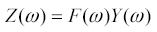
The tracking behavior of a PLL is equivalent to a linear filtering operation. The PLL acts like a low-pass filter. For example, in the racing game you track the low-frequency part of your opponent's motions. These are the long, slow, sweeping turns. You ignore the high-frequency behavior (the rapid shaking).
In the frequency domain, let the low-pass filter F ( w ) represent your tracking abilities , and let the function Y ( w ) represent the Fourier transform of your opponent's trajectory. The Fourier transform of your trajectory Z ( w ) is therefore a low-pass-filtered version of your opponent's trajectory:
Equation 12.10
|
where |
filter F ( w ) represents your tracking abilities, |
|
function Y ( w ) represents the Fourier transform of your opponent's trajectory, and |
|
|
function Z ( w )represents the Fourier transform of your trajectory. |
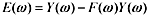
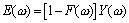
The tracking error E ( w ) is the difference between your motion and the motion of your opponent.
Equation 12.11
|
where |
function E ( w ) represents the Fourier transform of the tracking error. |
The tracking error may be expressed differently as a filter [1 “ F ( w )] applied to your opponent's trajectory.
Equation 12.12
|
where |
filter [1 “ F ( w )] represents the tracking-error filter function, |
|
function Y ( w ) represents the Fourier transform of your opponent's trajectory, and |
|
|
function E ( w ) represents the Fourier transform of your tracking error. |
If the filter F ( w ) is a low-pass filter, then the filter [1 “ F ( w )] must be a high-pass filter, in which case you may recognize that the tracking error is nothing more than the high-frequency part of your opponent's trajectory. It is a theorem of control systems analysis, therefore, that
The variance of the tracking error equals the variance of that part of your opponent's signal that falls above the tracking range of your filter .
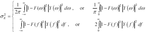
Applied to a PLL circuit, this theorem relates the power spectrum Y ( w ) 2 of the reference phase jitter, the gain of the tracking filter F ( w ), and the variance  of the tracking error:
Equation 12.13
|
where |
filter F ( w ) represents the gain of the tracking filter, |
|
function Y ( w ) represents the Fourier transform of the reference phase jitter, and |
|
|
|
 represents the variance of the tracking error.
Equation [12.13] appears in four formats. The top two formats integrate the power spectrum of the signal with respect to the frequency variable w , in rad/s. The bottom two formats integrate with respect to the frequency variable f , in Hertz, where 2 p f = w . The form of the integration is similar in both cases, but the constant term differs . This difference points out the importance of knowing whether the horizontal axis of a frequency-domain plot is expressed in units of rad/sec or Hertz.
In each row of [12.13], the left-hand expression shows integration over all positive and negative frequencies. This technique is called two-sided integration . The right-hand expressions shows integration over only positive frequencies with the results then doubled . The doubling trick works for the evaluation of power associated with real-valued signals, because the power spectrum of a real-valued signal is strictly real and an even function of w (or f ).
The following equations appear in only the top-right format, as one-sided integrations with respect to frequency w in rad/s. You may convert them to any of the four formats shown in [12.13].
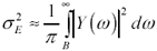
Equation [12.13] is often simplified by assuming filter F ( w ) is a perfect low-pass filter with a brick-wall cutoff at some frequency B ; in this case the integration need only be carried out from the cutoff frequency B to infinity. [124]
[124] A two-sided integration would carry from -
to - B , and then again from B to
Equation 12.14
|
where |
filter F ( w ) is assumed to have unity gain below B and zero gain above B , |
|
the cutoff frequency B is in rad/sec |
|
|
function Y ( w ) represents the Fourier transform of the reference phase jitter, and |
|
|
|
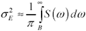
In cases where the reference signal is a stochastic signal (as opposed to a deterministic signal) the calculation [12.14] is modified as follows :
Equation 12.15
|
where |
function S ( w ) represents the spectral power density of the reference phase jitter, and |
|
|
The power spectrum S ( w ), already being a measure of power, does not need to be squared.
POINT TO REMEMBER
- The variance of the tracking error in a PLL circuit represents all the power in the input reference signal that falls above the tracking range of the PLL.
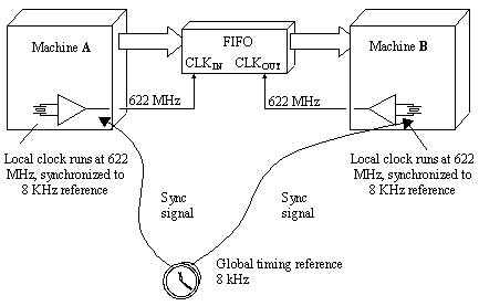
12.11.1.4 Clock Jitter in FIFO-Based Architectures
Suppose digital state machines A and B each independently use PLL circuits to synchronize their clocks to a common reference (Figure 12.57). Let the common reference frequency be 8 kHz. [125] The clock frequency in each section is 622 MHz, roughly 77,750 times the reference frequency. Data proceeds from section A , through the FIFO, into section B . Theoretically, once the FIFO gets started, it should stay filled at a constant level because the input and output rates are the same.
[125] A common telecommunications reference clock frequency.
In practice, however, the two clocks are hardly the same. The common timing reference signal comes along only once every 77,750 clocks, leaving plenty of time for the two clocks to diverge between reference edges. In the highway racing analogy, this architecture is the equivalent of putting a blindfold over your eyes and permitting you only one quick glimpse of the car in front once every 77,750 car lengths. Obviously, substantial errors may accumulate.
Short-term frequency variations between the two clocks cause the number of words held in the FIFO to gyrate wildly. In general, the greater the ratio of frequencies between the FIFO clock and the reference clock, the greater the gyrations. If the gyrations become too wild, the FIFO either overflows or runs empty.
The maximum deviation in the FIFO corresponds to the maximum phase difference between the two clocks, not the maximum frequency difference. Those familiar with the calculus of PLL circuits may recall that phase is the integral of the frequency. In other words, if the frequency difference between the two clocks diverges by x rad/s and holds at that level for t seconds, the accumulated phase difference during interval t would be xt . For example, a frequency offset of just one part in 10 4 , averaged over a period of 77,750 cycles, would result in 7.775 clocks of phase offset by the time the next clock arrived.
A good measure of performance in this system would be the frequency stability over a period of time T . The frequency stability D f may be defined as the worst-case difference between the minimum and maximum number of clock cycles within period T divided by the length of the period T . Appropriate units for D f are cycles/sec (Hz).
In burst-oriented systems the period of time T usually corresponds to one packet, or one complete data transaction. As long as the clocks don't drift with respect to each other more than N complete cycles within a packet, a FIFO of length 2 N is sufficient to couple the systems (where N = D fT ). [126]
[126] Preload at least N words into the FIFO before starting your transfer. If the receiver is fast, the FIFO will run completely dry at the end of the transfer. If the transmitter is fast, the FIFO will build to 2 N words by the end of the transfer.
PLL designers shudder when they see block diagrams like Figure 12.57. Reducing the ratio between the FIFO clock and the reference clock (i.e., distributing an 8 MHz reference instead of an 8 KHz reference) would significantly relax the requirements for PLL stability in this system.
Figure 12.57. Jitter between imperfectly synchronized high-speed clocks causes the number of words held in the FIFO to fluctuate.
POINT TO REMEMBER
- A large ratio between the reference clock frequency and the PLL output frequency requires a very stable VCO.
12.11.1.5 What Causes Jitter
Most oscillators include at least one resonant circuit (or delay element) and one amplifier (or comparator). Jitter in such an oscillator results from at least four superimposed noise sources. First, if you are using a crystal oscillator, noise emanates from the random movement of electrons within the crystal ( thermal noise) . [127] Second, any mechanical vibrations or perturbations of the crystal cause noise ( microphonic noise ). The third noise source stems from the amplifier or comparator used to construct the oscillator ( self-noise ). The amplifier's contribution is often larger than thermal and mechanical noise from a crystal. The last and potentially most troublesome noise comes from the power supply. Any coupling of an oscillator's power terminals to its sensitive amplifier input sends power supply noise roaring through the amplifier, causing massive amounts of jitter. An oscillator that couples power supply noise into its output is said to have poor power supply immunity . Many oscillators do.
[127] Oscillator circuits using LC tanks, delay lines, or semiconductor delay elements all display similar electrical and mechanical noise effects.
These four sources of noise appear together at the output of every oscillator or PLL circuit. Because an oscillator always involves feedback circuits, the same noise is also coupled back into the resonant circuit (or delay element) used to produce the oscillations in such a way that it influences future behavior. In this manner the noise causes both short-term and long-term frequency perturbations. The statistics of such fluctuations are beyond the scope of this book.
In addition to the intrinsic jitter from its internal oscillator, a PLL circuit will propagate any jitter from the reference source that falls within the tracking bandwidth of the PLL.
POINT TO REMEMBER
- Jitter in the output of a PLL comes from internal sources plus noise coupled from the power system and noise propagated from the reference input.
12.11.1.6 Random and Deterministic Jitter
Many circuits produce a repetitive, predictable jitter. This effect happens in cheesy clock-multiplier circuits and poorly equalized data recovery units. The predictable component of jitter in these circuits is called deterministic jitter. The remaining components of jitter are called random jitter. The presumption is usually made that the deterministic and random jitter components are not correlated ( [94] , [96] , and [97] ).
To measure the deterministic jitter on a clock (or data) waveform, you must trigger your oscilloscope at a rate commensurate with the source of the deterministic jitter. For example, in an 8B10B-coded data waveform transmitting a repetitive 10-bit test pattern, a trigger frequency of 1/10 the data baud rate would be appropriate. For another example, in a clock-multiplier circuit the input reference clock frequency would be appropriate.
The scope must be set to average its measured results, which nulls out all the random jitter, leaving you with a clean picture of a repetitive (though slightly distorted ) time-domain waveform. The deterministic jitter is the difference, at each transition in the repetitive sequence, between the actual time at which the transition occurred and the ideal time, in a perfect system, at which the transition should have occurred.
The vector of differences is processed to find the average value, and then the variance, of the measured points. This process puts you in possession of one piece of information: the variance of the deterministic jitter.
By measuring the variance of the overall jitter waveform (including both deterministic and random jitter) you can then infer the variance for the random jitter alone:
Equation 12.16

|
where |
|
 , and
, and  are the variances of the random, deterministic, and total components of jitter.
Deterministic jitter comes from many sources, including duty-cycle distortion (DCD), intersymbol interference (ISI), and word-synchronized distortion due to imperfections within a data serializer (e.g., bit 3 of each data word always appears early).
The point of separating jitter into random and deterministic components is that the deterministic components have a lower ratio of peak value to standard deviation than do the random components. Measured only according to the standard deviation, a certain amount of deterministic jitter doesn't hurt as much as a similar quantity of random jitter.
In a system that combines deterministic and random jitter, therefore, a single specification of the acceptable standard deviation of jitter will always be overly stringent.
Example Showing Calculation of Standard Deviation for Deterministic Jitter
I'll show the evaluation of standard deviation for a very simple case first, and then a more complicated one.
Let r represent a discrete random variable that takes on only two values, x 1 and x 2 , remaining at each value on average half the time.
The mean value of r is
The peak excursion of r on either side of the mean is
The variance of r is
The standard deviation of r (square root of variance) is
The ratio of peak magnitude to standard deviation is
Given a more complicated discrete random variable r that takes on values x i with probabilities p i , and has mean value m r , the variance of r is calculated
If r were distributed in a Gaussian manner, the peak magnitude could (theoretically) range upward without bound. In the analysis of practical systems the ratio of the effective peak magnitude to standard deviation is calculated depending on the BER (bit-error rate) at which the system must operate . Table 12.4 indicates the ratio of the effective peak magnitude to standard deviation for Gaussian waveforms assuming various standard BER values. The table values are computed such that the magnitude of Gaussian noise will not on average exceed the stated peak value more often than once every 1/BER bits.
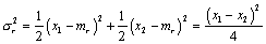

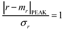
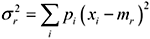
Table 12.4. Gaussian Waveform Probabilities
|
BER |
Ratio of peak deviation to standard deviation |
|---|---|
|
1E-04 |
3.891 |
|
1E-05 |
4.417 |
|
1E-06 |
4.892 |
|
1E-07 |
5.327 |
|
1E-08 |
5.731 |
|
1E-09 |
6.109 |
|
1E-10 |
6.467 |
|
1E-11 |
6.807 |
|
1E-12 |
7.131 |
|
1E-13 |
7.441 |
|
1E-14 |
7.739 |
Example Showing Acceptable Standard Deviation for Jitter
Assume you are willing to accept data errors at a BER of 1E-12. Make the worst-case assumption that all your jitter is Gaussian.
Under these assumptions, if your circuit can tolerate a peak phase error of 0.3 radian before making an error, then to achieve your target BER you must limit the standard deviation of total jitter to a level (according to Table 12.4) not exceeding 0.3/7.131 = 0.042 radians. For a system that combines random (Gaussian) and deterministic jitter, this specification is overly stringent.
To derive a better specification, first subtract from your worst-case total noise budget the known, worst-case amount of deterministic jitter. There is no need to multiply this component of jitter by 7.131 in the budget. It already represents a "worst-case" event.
Divide the remaining noise budget by 7.131 to establish a limit on the standard deviation of random jitter. The overall solution will meet your BER requirement.
For example, a specification calling for no more than 0.1 radian of deterministic noise plus random noise with a standard deviation not to exceed 0.028 radians meets the BER requirement of 1E-12 while providing a reasonable budget for deterministic noise.
POINT TO REMEMBER
- The point of separating jitter into random and deterministic components is to avoid overly stringent specifications for deterministic jitter.
12.11.2 Measuring Clock Jitter
There are many approaches to measuring clock jitter, including spectral analysis, direct phase measurement, differential phase measurement, BERT scan, and Timing Interval Analysis.
Spectral analysis is performed with a high-quality spectrum analyzer. The spectrum of a perfect clock consists of infinitely thin spectral peaks at harmonics of the fundamental frequency. Close examination of a jittery clock spectrum reveals a tiny amount of spreading around the fundamental frequency and around each harmonic . This spreading relates to clock jitter. Simply put, when a clock spends part of its time at frequency F , we see a peak there corresponding to what percentage of the time it lingered at that frequency. Spectral analysis is very popular with communications engineers .
The problem with spectral analysis is that it does not directly address the issue of phase error. The spectrum tells us what frequencies the clock visited but not how long it stayed. For example, a clock that lingers too long away from its center frequency accumulates a big phase error. A clock that deviates back and forth quickly about its center frequency may visit the same frequency for the same proportion of time, but stay so briefly each visit that it accumulates almost no phase error. From the spectrum alone, you cannot determine the maximum phase deviation from ideal unless you are willing to make the narrowband phase modulation assumption:
Assume the clock never deviates more than one radian from the ideal .
Under this assumption you can model a phase-modulated clock as if it were a perfect sinusoidal clock at frequency f to which you have added a small amount of noise, also at frequency f , like this:
Equation 12.17
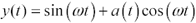
As long as a ( t ) remains less than one radian, the zero crossings of the signal [12.17] will occur at almost the same locations as in the following phase-modulated signal, where q ( t ) equals a ( t ).
Equation 12.18
Using [12.17] you can model any sinusoidal signal a ( t ) with small amounts of phase modulation as a combination of one main sinusoidal carrier plus another amplitude-modulated carrier at the same frequency, but in quadrature with the first signal. The instantaneous magnitude of the modulating signal a ( t ) is the same as the instantaneous phase jitter q ( t ), where q ( t ) is taken in units of radians.
What this all means is that when you look at the spectrum of a phase-jittery clock, what you see is one big whopping peak near the fundamental and a lower-level spreading of power around the peak. The big peak represents the power in the main sinusoidal carrier. The spreading represents the power present in the noise process a ( t )cos( w t ). The ratio of the power in the noise process a ( t )cos( w t ) to the total power in the main carrier precisely equals the variance of the phase jitter.
To obtain from the spectrum a maximum phase error (which is what one needs to solve certain FIFO problems), you must combine the power spectrum measurement with some assumption about the nature of the underlying probability distribution of the phase jitter. From the power spectrum measurement, you compute the variance of the distribution, and from knowledge of the properties of the assumed distribution, you may then compute the probability that the phase error q ( t ) will exceed some arbitrary limit (see "Jitter and Phase Noise" article below).
Direct phase measurement requires access to an ideal clock that is compared to your jittery clock with a phase detector. The phase detector output shows just what you want to know: how much the clock jitters. The obvious difficulty with this approach is getting an ideal clock. You might try filtering the jittery clock through a PLL to create a smooth clock having the same average frequency. The phase error output from the PLL will be the jitter signal you seek. This is known as the "golden PLL" method.
If you are measuring jitter from a high-quality frequency source, it may not be easy to build a golden PLL with significantly less intrinsic jitter than your source. This method develops difficulties when measuring phase errors that exceed the bit interval. To solve that problem, try working with a divided-down clock. Measured in units of clock intervals, an error of x in the main clock produces an error in a divided-by- n clock of only x / n .
Differential phase measurement compares a jittery clock not to an ideal clock but to a delayed version of itself. At a large enough delay, the delayed waveform may become uncorrelated with the original, giving you the effect of two similar, but different, jittery clocks. The resulting differential jitter is twice the actual jitter. The advantage of using a delayed version of the original clock is that it naturally has the correct average frequency.
A differential jitter measurement requires an oscilloscope with a delayed time-base sweep feature. First set your oscilloscope to trigger on the clock waveform. Then, using the delayed time-base sweep, take a close look at the clock some hundreds, thousands, or ten-thousands of clock cycles later. Jitter shows up as a blur in the displayed waveform.
Before assuming the blur comes from jitter on the clock, take a look at a stable clock source using the same setup. If it looks clean, you can then assume your scope time base is accurate enough to perform this measurement.
While adjusting the delay interval, you may notice that the jitter gets worse or better. This is normal. Clock jitter normally is worse in some frequency bands, which leads to maxima in the expected differential jitter at certain time delays. Beyond some maximum time delay, the jitter becomes completely uncorrelated and there is no longer any change in jitter with increasing delay.
If through some test procedure, you have intentionally created a large amount of jitter (i.e., FM-modulation of the clock) with a particular period T , the greatest jitter in the output will be observed at time T /2 (and successive odd multiples of T /2).
If the peak-to-peak amplitude of the phase jitter amounts to more than half a clock period, successive edges will blur together, becoming very difficult to see. In that case, divide the clock by 2, 4, or more using a counter circuit before displaying it. The division doesn't change the worst-case jitter on individual clock edges, but it does lengthen the space between nominal clock transitions so that you can see the jitter.
Jitter measurements on precise crystal clocks require an extremely stable time base and can take a long time to perform. Jitter measurements performed on noncrystal oscillators used in serial data transmission are much easier to do, owing to the much greater intrinsic jitter of those sources.
BERT scan measurements are used to quantify the jitter present on serial data transmission systems. In these methods a serial data stream with a known pseudorandom data pattern is fed into the BERT test instrument. The BERT contains a golden PLL capable of perfectly extracting an ( ideally ) zero-jitter clock from even the noisiest waveform. The golden PLL clock edge is adjustable within the data window.
The BERT attempts to recover the data, adjusting its ideal clock back and forth across the data window, producing a graph showing the bit-error rate as a function of the clock position. The bit-error rate graph thus produced is called a BER bathtub curve . It is so called because at either extreme, as the clock approaches the transition period leading to the next bit, the BER jumps to nearly unity, while in the middle of the curve there is (one would hope) a flat region of zero errors. The shape of the curve resembles a bathtub.
From the slope of the sides of the bathtub curve you may extract information about the statistics of jitter. The ANSI study [97] goes into great detail about the extrapolation of actual BER performance data based on limited measurements of BER bathtub curves.
Timing interval analysis accumulates a histogram of the intervals between successive clock (or data) edges. For example, an accumulation of the histogram of the fine variations in spacing between clock edges separated by a large interval T is equivalent to the information gathered by a differential phase measurement at delay T , but with the advantage that the data is recorded in a form from which the statistics may be easily derived.
Of all the types of measurements mentioned, the manufacturers of time-interval analysis equipment seem most interested in providing tools and software useful for the analysis of jitter.
PLL loop testing is possible if the oscillator under test is controllable with an input voltage. This test uses the oscillator under test as the VCO in an artificially constructed laboratory-grade PLL. An ideal clock is fed into the artificial VCO as a reference. The loop bandwidth of the artificial PLL must be much less than the bandwidth of the VCO phase jitter that you propose to measure.
The PLL structure eliminates low-frequency wander in the oscillator under test, making it easier to see the phase jitter of interest. The output of the artificial PLL phase detector (with a suitable low-pass filter) is your direct phase error measurement. This output can be observed using a low-bandwidth spectrum analyzer or oscilloscope with FFT processing. This approach is very closely related to the golden PLL method described previously.
12.11.2.1 Jitter Measurement
POINT TO REMEMBER
- The noise properties of a PLL are characterized by the intrinsic internal jitter, the power supply sensitivity, and a jitter transfer function.
12.11.2.2 Jitter and Phase Noise
[128] To find the total power you must integrate over both positive and negative frequencies. Alternately, you can just integrate over only positive frequencies (one-sided integration) and then double the result. If all you want are ratios, then you may skip the doubling.
POINT TO REMEMBER
- You can calculate the variance of jitter using a spectrum analyzer.
Fundamentals
- Impedance of Linear, Time-Invariant, Lumped-Element Circuits
- Power Ratios
- Rules of Scaling
- The Concept of Resonance
- Extra for Experts: Maximal Linear System Response to a Digital Input
Transmission Line Parameters
- Transmission Line Parameters
- Telegraphers Equations
- Derivation of Telegraphers Equations
- Ideal Transmission Line
- DC Resistance
- DC Conductance
- Skin Effect
- Skin-Effect Inductance
- Modeling Internal Impedance
- Concentric-Ring Skin-Effect Model
- Proximity Effect
- Surface Roughness
- Dielectric Effects
- Impedance in Series with the Return Path
- Slow-Wave Mode On-Chip
Performance Regions
- Performance Regions
- Signal Propagation Model
- Hierarchy of Regions
- Necessary Mathematics: Input Impedance and Transfer Function
- Lumped-Element Region
- RC Region
- LC Region (Constant-Loss Region)
- Skin-Effect Region
- Dielectric Loss Region
- Waveguide Dispersion Region
- Summary of Breakpoints Between Regions
- Equivalence Principle for Transmission Media
- Scaling Copper Transmission Media
- Scaling Multimode Fiber-Optic Cables
- Linear Equalization: Long Backplane Trace Example
- Adaptive Equalization: Accelerant Networks Transceiver
Frequency-Domain Modeling
- Frequency-Domain Modeling
- Going Nonlinear
- Approximations to the Fourier Transform
- Discrete Time Mapping
- Other Limitations of the FFT
- Normalizing the Output of an FFT Routine
- Useful Fourier Transform-Pairs
- Effect of Inadequate Sampling Rate
- Implementation of Frequency-Domain Simulation
- Embellishments
- Checking the Output of Your FFT Routine
Pcb (printed-circuit board) Traces
- Pcb (printed-circuit board) Traces
- Pcb Signal Propagation
- Limits to Attainable Distance
- Pcb Noise and Interference
- Pcb Connectors
- Modeling Vias
- The Future of On-Chip Interconnections
Differential Signaling
- Differential Signaling
- Single-Ended Circuits
- Two-Wire Circuits
- Differential Signaling
- Differential and Common-Mode Voltages and Currents
- Differential and Common-Mode Velocity
- Common-Mode Balance
- Common-Mode Range
- Differential to Common-Mode Conversion
- Differential Impedance
- Pcb Configurations
- Pcb Applications
- Intercabinet Applications
- LVDS Signaling
Generic Building-Cabling Standards
- Generic Building-Cabling Standards
- Generic Cabling Architecture
- SNR Budgeting
- Glossary of Cabling Terms
- Preferred Cable Combinations
- FAQ: Building-Cabling Practices
- Crossover Wiring
- Plenum-Rated Cables
- Laying Cables in an Uncooled Attic Space
- FAQ: Older Cable Types
100-Ohm Balanced Twisted-Pair Cabling
- 100-Ohm Balanced Twisted-Pair Cabling
- UTP Signal Propagation
- UTP Transmission Example: 10BASE-T
- UTP Noise and Interference
- UTP Connectors
- Issues with Screening
- Category-3 UTP at Elevated Temperature
150-Ohm STP-A Cabling
- 150-Ohm STP-A Cabling
- 150- W STP-A Signal Propagation
- 150- W STP-A Noise and Interference
- 150- W STP-A: Skew
- 150- W STP-A: Radiation and Safety
- 150- W STP-A: Comparison with UTP
- 150- W STP-A Connectors
Coaxial Cabling
- Coaxial Cabling
- Coaxial Signal Propagation
- Coaxial Cable Noise and Interference
- Coaxial Cable Connectors
Fiber-Optic Cabling
- Fiber-Optic Cabling
- Making Glass Fiber
- Finished Core Specifications
- Cabling the Fiber
- Wavelengths of Operation
- Multimode Glass Fiber-Optic Cabling
- Single-Mode Fiber-Optic Cabling
Clock Distribution
- Clock Distribution
- Extra Fries, Please
- Arithmetic of Clock Skew
- Clock Repeaters
- Stripline vs. Microstrip Delay
- Importance of Terminating Clock Lines
- Effect of Clock Receiver Thresholds
- Effect of Split Termination
- Intentional Delay Adjustments
- Driving Multiple Loads with Source Termination
- Daisy-Chain Clock Distribution
- The Jitters
- Power Supply Filtering for Clock Sources, Repeaters, and PLL Circuits
- Intentional Clock Modulation
- Reduced-Voltage Signaling
- Controlling Crosstalk on Clock Lines
- Reducing Emissions
Time-Domain Simulation Tools and Methods
- Ringing in a New Era
- Signal Integrity Simulation Process
- The Underlying Simulation Engine
- IBIS (I/O Buffer Information Specification)
- IBIS: History and Future Direction
- IBIS: Issues with Interpolation
- IBIS: Issues with SSO Noise
- Nature of EMC Work
- Power and Ground Resonance
Points to Remember
Appendix A. Building a Signal Integrity Department
Appendix B. Calculation of Loss Slope
Appendix C. Two-Port Analysis
- Appendix C. Two-Port Analysis
- Simple Cases Involving Transmission Lines
- Fully Configured Transmission Line
- Complicated Configurations
Appendix D. Accuracy of Pi Model
Appendix E. erf( )
Notes
EAN: N/A
Pages: 163
