LVDS Signaling
This section is not intended as a promotion of LVDS logic. It is a primer on how to interpret the specifications of any differential logic family.
Low-Voltage Differential Signaling (LVDS) is a good example of a high-speed differential logic family. The LVDS standard was generated in 1995 by the IEEE. [62]
The LVDS standard contemplates both general-purpose and short-range applications. Here I will confine my remarks to the general-purpose version of the standard. It defines a differential data path operating at data transfer rates in the range of 200 to 500 MHz with a source-synchronous clock and various bus widths up to 128 bits.
Table 6.5 lists some of the key performance specifications for LVDS general-purpose transceivers.
6.13.1 Output Levels
LVDS being a differential logic family, there are two (complementary) outputs per logic signal. The nominal steady-state operating conditions for these outputs are 1.0 and 1.4 volts, for the low and high states respectively. When one wire goes to 1.0 volts , the other goes to 1.4, and vice versa.
Table 6.5. LVDS General-Purpose Link Specs ( adapted from ANSI/IEEE P1596-3-1995)
|
Transmitter specifications |
|||||
|---|---|---|---|---|---|
|
Signal |
Parameter |
Conditions |
Min |
Max |
units |
|
V oh |
Output voltage high, either wire |
R load = 100 W ± 1% |
1475 |
mV |
|
|
V ol |
Output voltage low, either wire |
R load = 100 W ± 1% |
925 |
mV |
|
|
V od |
Output differential voltage |
R load = 100 W ± 1% |
250 |
400 |
mV |
|
R |
Output impedance, single-ended |
V cm =1.0V and 1.4V |
40 |
140 |
W |
|
V os |
Output offset voltage |
1125 |
1275 |
mV |
|
|
D V os |
Change in VOS between 0 and 1 states (this specification defines the AC common-mode output voltage) |
R load = 100 W ± 1% |
25 |
mV |
|
|
t rise , t fall |
V od rise/fall time 20% to 80% |
R load = 100 W ± 1% |
300 |
500 |
ps |
|
Receiver specifications |
|||||
|
V i |
Input voltage range, either input |
V gpd < 925 mV |
2400 |
mV |
|
|
V idth |
Input differential threshold |
V gpd < 925 mV |
“100 |
+100 |
mV |
|
V hyst |
Input differential hysteresis |
V idthh “ V idthl |
25 |
mV |
|
|
R in |
Receiver differential input impedance |
” |
90 |
110 |
W |
|
C in |
Not specified |
||||
|
Implementation specifications |
|||||
|
Pcb skew allocation |
Worst case |
50 |
ps |
||
You may decompose this situation into a steady-state common-mode component of 1.2 volts, plus a changing differential voltage of ±0.4 volts. [57] The differential voltage varies from “0.4 V to +0.4 V, so we say that the differential peak-to-peak voltage is 800 mV. The peak-to-peak voltage on either wire alone would be 400 mV.
[57] Or an even-mode voltage of 1.2 volts plus an odd-mode voltage of ±0.2 volts.
The standard requires that the steady-state differential voltage representing either a zero or one state be at least 250 mV, but no larger than 400 mV when the outputs are loaded differentially by 100 ohms . It also requires that no output ever fall below 925 mV or exceed 1475 mV under the same conditions.
Concerning output levels under other loading conditions, the standard provides little guidance. The only hints come in the form of stated constraints on output impedance. From the standard it is impossible to determine, for example, the output levels that would result from loading the outputs with a 75-ohm differential load. Nor is it possible to determine something else that the IBIS community has long sought in these sorts of documents: a precise specification of the shape of the rising and falling edge.
POINT TO REMEMBER
- Normal operating voltages for LVDS logic are 1.2 ± 0.2 V on each wire.
6.13.2 Common-Mode Output
The output offset voltage (DC bias) can change by 25 mV when switching from the one state to the zero state. This is a peak-to-peak change. The AC amplitude range of the common-mode voltage is therefore ±12.5 mV.
The AC amplitude of the differential output voltage lies somewhere in the range of ±250 to ±400 mV.
When considering certain radiation and crosstalk problems, it is handy to know the approximate ratio between common-mode and differential-mode emissions coming out of a driver. For LVDS, the ratio of common to differential amplitudes can be as poor as 12.5/250 = 5%.
POINT TO REMEMBER
- LVDS, like most digital transceivers, is not extraordinarily well balanced.
6.13.3 Common-Mode Noise Tolerance
Looking at the common-mode operating range of the receiver (called V i in the specification), it is apparent that the receiver can tolerate inputs anywhere in the range of 0 to 2400 mV. From these numbers you can derive how much common-mode noise the system will tolerate. First assume a driver is at its lowest permissible level (925 mV). Now figure out how much common-mode noise you can add in the negative direction without the receiver input falling outside its guaranteed operating range. The answer is “925 mV. Next assume the driver is at its highest permissible level (1475 mV). Now figure out how much common-mode noise you can add in the positive direction without the input falling outside its guaranteed operating range. The answer is +925 mV. LVDS therefore tolerates a common-mode difference ( V gpd ) between the ground potential at the driver and the ground potential at the receiver as great as ±925 mV.
If you exceed the common-mode operating range of the receiver, all bets are off. It could do anything (see Section 6.7, "Common-Mode Range").
POINT TO REMEMBER
- The common-mode noise tolerance for general-purpose LVDS logic is ±925 mV.
6.13.4 Differential-Mode Noise Tolerance
Next let's look at the differential noise margin. In the worst case the transmitter differential output may be as small as 250 mV. At the same time, the receiver threshold may be offset by as much as 100 mV. The difference between these two figures is the differential noise margin, which is 150 mV. As a percentage of the signal swing on either wire (400 mV p-p), the 150 mV figure represents 37%. A transmitter with a larger output swing would enjoy an even bigger percentage noise margin. These are excellent noise margins for digital logic. Most single-ended logic families have noise margin percentages on the order of only 10% to 15%.
POINT TO REMEMBER
- The high noise margin gives LVDS a built-in natural advantage in combating ringing, overshoot, and crosstalk from like devices.
6.13.5 Hysteresis
A receiver with hysteresis has two input switching thresholds, one used for positive-going signals and one used for negative-going signals. The positive-going threshold is always set a little higher than the negative-going threshold. Once the input crosses into positive territory, the receiver automatically switches to the negative-going threshold so that the signal must turn around and descend below the negative threshold before it can cause another switching event. Once the signal crosses below the negative threshold, the receiver flips back to using the positive threshold. A receiver equipped with hysteresis requires a certain amount of signal change before flipping to the other state.
The hysteresis feature is intended to avoid annoying self-oscillation that might happen with slowly changing, but very clean, inputs. The feature is usually implemented as a form of limited positive feedback from the receiver output back to own its input. With hysteresis, the inputs tend to switch quickly and firmly, once they reach an acceptable level, and then stay there. It's a good feature.
LVDS inputs have a guaranteed amount of hysteresis. You still, however, shouldn't supply any of these parts with a slowly moving input, because in that case as the input slowly sweeps through the transition region, any crosstalk that happens to exceed the hysteresis switching range will cause glitches (and therefore more noise) in the receiver.
POINT TO REMEMBER
- Always provide fast-edged inputs to LVDS logic.
6.13.6 Impedance Control
The LVDS specification goes to a lot of trouble to control ringing and reflections. This is one of the strongest provisions of the specification. Excellent control of ringing and reflections makes it possible to obtain first-incident-wave switching in most LVDS applications.
LVDS uses a both-ends termination strategy to control reflections. Each LVDS transmission line is terminated first at the source and again at the end of the line. [58]
[58] Variants of LVDS are available in which the drivers can enter a tri-state (high-impedance) mode, and the receivers do not incorporate terminations. These versions are suitable for building multidrop bus structures.
The source impedance of the driver is constrained to the range of 40 to 140 W . That is a ratio of only 3.5:1 from highest value of allowed output impedance to the lowest. To a board-level analog designer, this sounds easy, because you can go out and buy very accurate lumped-element resistors. To a chip designer, it's a nightmare. You just can't control the absolute value of R DS (ON) or the absolute value of transconductance very accurately.
The achievement of a 3.5:1 output impedance specification represents a major accomplishment for the chip industry, one which I am sure will pay off in terms of higher volume, given the user -friendly advantages of both-ends termination (see box "Both-Ends Termination").
The worst-case reflection coefficient at the transmitter, assuming it is coupled to a perfect 100- W transmission line, will therefore be the worse of these two numbers:
Equation 6.26
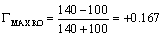
Equation 6.27
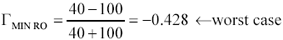
The input impedance of the receiver is constrained to the range 90 to 110 W . The LVDS specification recommends (but does not require) that this be implemented as a built-in terminator, placed inside the integrated chip package right at the die. From a signal integrity perspective, that would definitely be the best place to put it. Initial LVDS implementations, however, did not do this. Due in part to the difficulty of fabricating accurate on-chip resistances, early implementations of LVDS left the 100-ohm termination as an external component.
If you have to design with external terminations, use a 100- W ±10% external terminating resistor in a low-inductance package (0805 or smaller package) directly attached to the transmission line at the input terminals of the package, with very small pads (for low parasitic capacitance ). [59]
[59] Smaller components , if properly installed, have less parasitic series inductance and also less parasitic shunt capacitance, than larger ones. There is an electromagnetic theorem that says that if you shrink a configuration (component and layout together) in all three physical dimensions by a factor of k , then the inductance of that configuration also shrinks by a factor of k . If, as is common, you shrink the component length and breadth by factor k but do not change the height (i.e., the spacing from surface layer to the underlying reference plane), then the inductance shrinks, but not by a factor of quite as much as k (more like k 2/3 ).
The worst-case reflection at the terminator, assuming a line impedance of precisely 100 W , will be the worse of these two numbers:
Equation 6.28
Equation 6.29
Multiplying together the worst-case transmitter and receiver reflection coefficients, G MIN RO [6.27] and G MIN RIN [6.29], shows that the amplitude of any residual reflections in the transmission structure (meaning anything that arrives after the initial step edge) can in no case exceed 2.25% of the initial signal amplitude. Therefore, you can expect solid first-incident wave switching performance from this system, assuming a perfect implementation with perfect 100- W differential transmission lines.
You may be wondering how far the line impedance may stray from the ideal value of 100- W while still guaranteeing first-incident-wave switching. Figure 6.34 reveals the answer. This figure shows the magnitude of the residual reflections remaining after the arrival of the first-incident waveform. The figure is a compilation of four different constraint lines corresponding to different combinations of worst-case high and low R o interacting with worst-case high and low R in . At various specific values of trace impedance, one constraint or another takes precedence, which accounts for the segmented appearance of the curve.
Figure 6.34. Residual reflection after arrival of initial step edge for terminated LVDS logic with worst-case transmitter and receiver impedances, as a function of trace impedance.
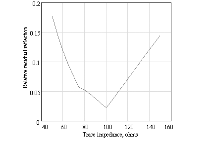
The chart indicates that a line impedance of 100 W ±10 would produce an initial residual reflection no greater than 5% of the incoming step amplitude. A plus-or-minus 20-ohm tolerance would increase the initial residual to no greater than 7%. LVDS logic, because it uses a both-ends style termination, tolerates a fairly wide range of line impedances.
The existence of a significant residual reflection may not by itself endanger the performance of a particular link, depending on the polarity and timing of the arrival of the reflected signal power. Only time-domain simulation can tell.
This figure assumes the transmitter and receiver impedances are purely resistive. Any significant reactances at either the transmitter or receiver will further degrade the performance.
POINT TO REMEMBER
- LVDS works best with 100- W transmission lines.
6.13.7 Trace Radiation
In the LVDS specification the number D V OS defines the degree of balance between the two complementary outputs. It calls for a peak-to-peak common-mode (or even-mode) content in the transmitted signal of no more than 25 mV. Compared to the peak-to-peak signal level on either of the two signal wires (400 mV), that's a relative common-mode content of 6.25%.
The common-mode content limits the degree of attainable radiated field cancellation to a value of “24 dB (=20log(0.0625)). You can easily achieve this amount of cancellation at all frequencies up to 1 GHz by placing the differential traces at any separation of 0.5 mm or less (see Section 6.11.3). Unless you need to save the circuit board space, it is not, in this author's opinion, worth the effort trying to cram LVDS traces closer together than 0.5 mm.
In individual circumstances with particularly well-balanced transmitters it is possible to get better cancellation, but you can't depend on always having parts that beat the specification.
POINT TO REMEMBER
- You need not struggle to place ordinary differential digital traces any closer than 0.5 mm (0.020 in.) for any EMI purpose.
6.13.8 Risetime
I'm glad to see a specification for the minimum risetime. That' s a big help when dealing with all manner of high-speed phenomena, especially the calculation of crosstalk. I offer my sincere thanks to all the standards weanies who voted for this provision.
6.13.9 Input Capacitance
The last of the receiver specifications is the input capacitance. Sadly, this specification is lacking. The closest we get in the standard to addressing the input capacitance is a vague statement that the input capacitance "should not limit the high-frequency, 250-MHz operation of the receiver." That's nice, but it's not a specification. Standards like this leave open the possibility of receivers that meet the spec as written, but don't interoperate .
6.13.10 Skew
The LVDS committee did a lot of work on clock-to-data skew. They carved out an overall skew budget, defining a permissible amount of skew for each signal in an LVDS link. Their budget assumes a link architecture that includes two pcbs, each with a connector and each plugged into some sort of backplane media.
In this architecture the specification pcb designers need to worry about is the pcb skew number of 50 ps. If every data and clock signal in an LVDS link is matched to within this amount of delay, the timing for the link as a whole should work.
Keep in mind that skew accumulates as your signal progresses. If your signal must traverse more than two connectors, the skew budget for each is less than in a simpler system.
If you are using an FR-4 dielectric, the 50-ps delay number gives you an allowance for about 1/4 inch of line length imbalance between any two signals in an LVDS link. This figure is definitely achievable, but don't depend entirely on your autorouter ”you need to take a close look at the final artwork to make sure you've stayed under the limit.
The LVDS specification does not make any specific reference to the degree of skew imbalance permitted between the two wires of an individual differential signal. My rule of thumb is that the skew imbalance in any differential pair should be kept to less than 1/10 of the risetime.
POINT TO REMEMBER
- Always double-check your final artwork to make sure you've met the specifications for skew.
6.13.11 Fail-Safe
LVDS components from National Semiconductor include a fail-safe circuit in the receivers. This feature shuts off the output in the event the input is disconnected (zero differential input). This feature is permitted by the standard, but not required, so check carefully if you will be mixing different vendors to make sure they all do it in a compatible fashion.
Figure 6.35 illustrates how fail-safe is implemented in the National LVDS logic family.
Figure 6.35. Switching levels for National LVDS logic family.
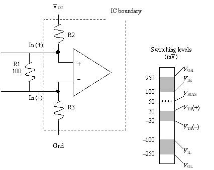
The figure depicts the mandated differential thresholds, V IH and V IL , for an LVDS receiver. The manufacturer of the receiver in Figure 6.35 has created a part with better control over the input threshold than the mandated minimum. The actual thresholds, V TH (+) and V TH ( “), are specified at ±30 mV. The close tolerance of the actual thresholds is exploited to create the fail-safe feature.
The fail-safe feature is created by forward biasing the inputs. When the input is disconnected from any source (the transmitter is turned off or unplugged), biasing resistors R2 and R3 trickle enough current through the external end-termination resistor R1 to forward-bias the input by 50 mV. This level is above the actual component threshold, so the receiver output stays locked at 1.
When the input is connected to a source with a differential output impedance of 100 ohms, the current from resistors R2 and R3 forward-biases the input by only half as much, or only about 25 mV, shifting V TH (+) and V TH ( “) to new worst-case values of +55 mV and “5 mV respectively. These values remain well within the mandated limits of ±100 mV.
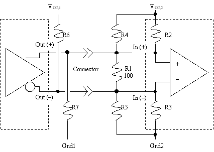
Some applications require a greater margin of safety for the fail-safe feature. For example, let's say you are making a twisted-pair communication link. When the transmitter is powered off, you may expect more than 25 mV of differential noise. This can be implemented by adding two new resistors, R4 and R5, in parallel with the existing bias resistors R2 and R3, but outboard of the IC package. The new resistors can be sized to enforce an arbitrary amount of offset in the case the transmitter is disconnected. One disadvantage of this technique, if taken to an extreme, is that the fail-safe bias current may be large enough to disturb normal operations.
The circuit in Figure 6.36 fixes this problem. In the event the transmitter is powered off or unplugged, the fail-safe resistors R4 and R5 provide a large amount of bias current. In the event the transmitter is connected and powered on, you can pick values for R6 and R7 in the transmitter that will source an equal and opposite amount of current, canceling the offset. Resistors R2 through R5 appear in parallel with the differential impedance of the termination network and must be taken into account when selecting values for R1 and trace impedance. The same applies for resistors R6 and R7 at the source.
Figure 6.36. Combining external bias resistors at receiver and transmitter creates zero bias during operational mode.
POINT TO REMEMBER
- Fail-safe features are permitted by the LVDS standard, but not required .
For further study see: www.sigcon.com
Fundamentals
- Impedance of Linear, Time-Invariant, Lumped-Element Circuits
- Power Ratios
- Rules of Scaling
- The Concept of Resonance
- Extra for Experts: Maximal Linear System Response to a Digital Input
Transmission Line Parameters
- Transmission Line Parameters
- Telegraphers Equations
- Derivation of Telegraphers Equations
- Ideal Transmission Line
- DC Resistance
- DC Conductance
- Skin Effect
- Skin-Effect Inductance
- Modeling Internal Impedance
- Concentric-Ring Skin-Effect Model
- Proximity Effect
- Surface Roughness
- Dielectric Effects
- Impedance in Series with the Return Path
- Slow-Wave Mode On-Chip
Performance Regions
- Performance Regions
- Signal Propagation Model
- Hierarchy of Regions
- Necessary Mathematics: Input Impedance and Transfer Function
- Lumped-Element Region
- RC Region
- LC Region (Constant-Loss Region)
- Skin-Effect Region
- Dielectric Loss Region
- Waveguide Dispersion Region
- Summary of Breakpoints Between Regions
- Equivalence Principle for Transmission Media
- Scaling Copper Transmission Media
- Scaling Multimode Fiber-Optic Cables
- Linear Equalization: Long Backplane Trace Example
- Adaptive Equalization: Accelerant Networks Transceiver
Frequency-Domain Modeling
- Frequency-Domain Modeling
- Going Nonlinear
- Approximations to the Fourier Transform
- Discrete Time Mapping
- Other Limitations of the FFT
- Normalizing the Output of an FFT Routine
- Useful Fourier Transform-Pairs
- Effect of Inadequate Sampling Rate
- Implementation of Frequency-Domain Simulation
- Embellishments
- Checking the Output of Your FFT Routine
Pcb (printed-circuit board) Traces
- Pcb (printed-circuit board) Traces
- Pcb Signal Propagation
- Limits to Attainable Distance
- Pcb Noise and Interference
- Pcb Connectors
- Modeling Vias
- The Future of On-Chip Interconnections
Differential Signaling
- Differential Signaling
- Single-Ended Circuits
- Two-Wire Circuits
- Differential Signaling
- Differential and Common-Mode Voltages and Currents
- Differential and Common-Mode Velocity
- Common-Mode Balance
- Common-Mode Range
- Differential to Common-Mode Conversion
- Differential Impedance
- Pcb Configurations
- Pcb Applications
- Intercabinet Applications
- LVDS Signaling
Generic Building-Cabling Standards
- Generic Building-Cabling Standards
- Generic Cabling Architecture
- SNR Budgeting
- Glossary of Cabling Terms
- Preferred Cable Combinations
- FAQ: Building-Cabling Practices
- Crossover Wiring
- Plenum-Rated Cables
- Laying Cables in an Uncooled Attic Space
- FAQ: Older Cable Types
100-Ohm Balanced Twisted-Pair Cabling
- 100-Ohm Balanced Twisted-Pair Cabling
- UTP Signal Propagation
- UTP Transmission Example: 10BASE-T
- UTP Noise and Interference
- UTP Connectors
- Issues with Screening
- Category-3 UTP at Elevated Temperature
150-Ohm STP-A Cabling
- 150-Ohm STP-A Cabling
- 150- W STP-A Signal Propagation
- 150- W STP-A Noise and Interference
- 150- W STP-A: Skew
- 150- W STP-A: Radiation and Safety
- 150- W STP-A: Comparison with UTP
- 150- W STP-A Connectors
Coaxial Cabling
- Coaxial Cabling
- Coaxial Signal Propagation
- Coaxial Cable Noise and Interference
- Coaxial Cable Connectors
Fiber-Optic Cabling
- Fiber-Optic Cabling
- Making Glass Fiber
- Finished Core Specifications
- Cabling the Fiber
- Wavelengths of Operation
- Multimode Glass Fiber-Optic Cabling
- Single-Mode Fiber-Optic Cabling
Clock Distribution
- Clock Distribution
- Extra Fries, Please
- Arithmetic of Clock Skew
- Clock Repeaters
- Stripline vs. Microstrip Delay
- Importance of Terminating Clock Lines
- Effect of Clock Receiver Thresholds
- Effect of Split Termination
- Intentional Delay Adjustments
- Driving Multiple Loads with Source Termination
- Daisy-Chain Clock Distribution
- The Jitters
- Power Supply Filtering for Clock Sources, Repeaters, and PLL Circuits
- Intentional Clock Modulation
- Reduced-Voltage Signaling
- Controlling Crosstalk on Clock Lines
- Reducing Emissions
Time-Domain Simulation Tools and Methods
- Ringing in a New Era
- Signal Integrity Simulation Process
- The Underlying Simulation Engine
- IBIS (I/O Buffer Information Specification)
- IBIS: History and Future Direction
- IBIS: Issues with Interpolation
- IBIS: Issues with SSO Noise
- Nature of EMC Work
- Power and Ground Resonance
Points to Remember
Appendix A. Building a Signal Integrity Department
Appendix B. Calculation of Loss Slope
Appendix C. Two-Port Analysis
- Appendix C. Two-Port Analysis
- Simple Cases Involving Transmission Lines
- Fully Configured Transmission Line
- Complicated Configurations
Appendix D. Accuracy of Pi Model
Appendix E. erf( )
Notes
EAN: N/A
Pages: 163
