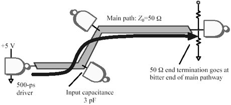
Daisy-Chain Clock Distribution
The daisy-chain configuration illustrated in Figure 12.46 distributes one clock signal to multiple receivers. Provided that the receivers do not distort the transmitted signal as it passes by in front of them, the signal should slide cleanly down the structure, delivering an unmolested copy of the original transmitted waveform to each receiver, only with increasing delay as the signal approaches the endpoint.
Figure 12.46. A daisy-chain connection works only if the taps do not distort the signal passing along the main path .
Unfortunately, as the signal passes along the main path, each tap generates a small negative reflection. The duration of the reflected pulse is roughly equal to the rise (or fall) time of the incoming signal, and the amplitude of the pulse is approximately given by equation [12.7] (see also Section 5.3.1.2, "Pcb: Lumped-Element Reflections").
The reflected pulses propagate backwards along the line toward the source end of the line. At the source, these pulses bounce off the driver, returning later to the far end of the line where they interfere with reception .
Example Showing Pulses Reflected from Daisy-Chain Load
t r
10% to 90% risetime of the driver = 500 ps
D V
amplitude of the incoming step = 2.5V
C
lumped-element capacitance = 3 pF
Z
characteristic impedance of transmission line = 50 W
t
time constant (1/2) Z C = 75ps
The peak amplitude a of the reflected pulse is given approximately by
Equation 12.7
The reflected pulse amplitude amounts to 15% of the signal swing. This is enough to preclude first-incident wave switching with many logic families. To achieve first-incident-wave switching (a requirement for clock signals), each rising edge must immediately proceed to a level above V IH and stay there, and each falling edge must drop below V IL and stay there. Assuming on the falling edge a worst-case (max) V OL from the driver, a late reflection magnitude of 15% could for many single-ended logic families pop the signal back up across the V IL threshold, causing double-clocking.
Five means of reducing the reflected pulse height and thereby improving the system step response, are
Slow the risetime of the driver. According to [12.7], this directly shrinks the reflected pulse. This item points out a prime disadvantage of using logic too fast for your application. The optimum driver for any clock distribution application is just fast enough to meet your clock skew budget, but no faster.
Lower the capacitance of each tap. This reduces the value of the intermediate time constant t . To the load capacitance, you also need to add the parasitic capacitance of any connectors and the capacitance of any pc trace stub leading to the receiver.
Lower the characteristic impedance of the clock distribution line. This method also reduces the value of the intermediate time constant t . The lowest valued end termination a driver can safely operate while meeting V OH and V OL on every edge equals the spread between the datasheet values of its V OH and V OL divided by the spread between its I OH and I OL .
Isolate each receiver from the bus with a series resistor having a value at least as large as the characteristic impedance of the line. The resistor presents a higher impedance load to the daisy chain, reducing reflections on the main pathway , but degrading the risetime of the signal at each receiver. CMOS circuits, which draw very little DC bias current, work well with this approach. Bipolar circuits that require larger amounts of input current do not.
Compensate for the capacitance at each tap by adjusting the trace width near the tap. This approach is discusses further in the examples below and in Section 5.3.1.3, "Potholes."
POINT TO REMEMBER
- Five things reduce the reflection from an isolated, lumped-element capacitive load: slow the risetime, lower the capacitance, lower the characteristic impedance of the trace, isolate the load with a big resistor, or compensate for the capacitance by modulating the trace width.
12.10.1 Case Study of Daisy-Chained Clock
This section examines in minute detail the distributed effect of multiple loads daisy-chained on a clock net. The clock source drives five loads. They are interconnected using an FR-4 stripline daisy chain. Each load is separated by 5 cm from its neighbor (for a raw trace delay between loads of 345 ps). Each load has 3 pF of input capacitance. The driver has a 10- W output impedance and a 500-ps rise/fall time.
Figure 12.47 demonstrates the effect of just one of the loads on the step response of the stripline. In the figure the overall length of trace simulated is 25 cm (10 in.). The figure reveals the relationship between voltage and time as observed at six discrete positions along the line, corresponding to distances of 0, 5, 10, 15, 20, and 25 cm from the source. These positions correspond to the locations of the source and the five loads to be placed on the structure.
Figure 12.47. A long, uniform transmission line with one capacitive load displays lumps in its step response.
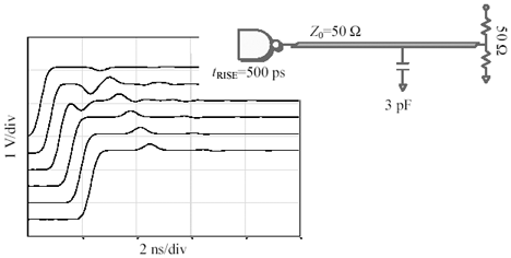
The previous example concluded that the size of the reflections generated by a 3-pF load under similar conditions should be about 15% of the signal swing. That value agrees generally with the size of the worst of the humps and lumps in the waveforms depicted in Figure 12.47. Equation [12.7] is a reasonable approximation for loads widely separated in comparison to the length of your signal's rise or fall time.
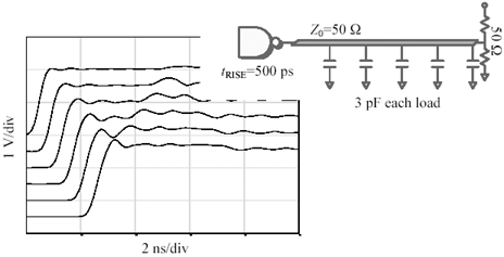
In Figure 12.48 the circuit is now burdened with all five loads. Did you expect the signals to look five times worse ? They don't. Part of the reason the signals look so good is because in this particular topology the signal risetime of 500 ps exceeds the trace delay between the taps of 345 ps. In systems where the risetime exceeds the tap spacing the signal begins to perceive the loads not as individual potholes, but more as a continuum of capacitance distributed uniformly along the transmission structure. I imagine in this case each rising or falling edge surfing along the loads, hitting the tops but not falling into the troughs.
Figure 12.48. In this particular topology adding four more loads doesn't much worsen the signal waveform.
I can exaggerate the surfing effect by switching to a different driver with a slower risetime. Figure 12.49 illustrates the effect of a slower, 1000-ps driver. Its output signal is so slow it averages together the actions of several loads at a time as it surfs down the structure.
Figure 12.49. A slower risetime averages together the effect of the individual loads, smoothing out the ripples.
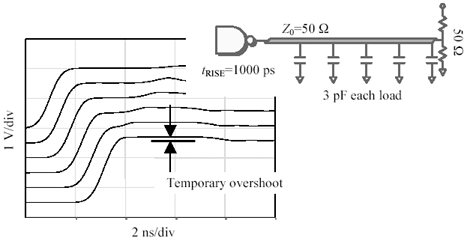
Now that the signal is somewhat smoothed out, a new artifact becomes visible. At the far end of the line (bottommost waveform in Figure 12.49) the signal appears to initially overshoot by about 10%, but then after one round-trip delay, the signal falls back to a normal amplitude. Overshoot in an end- terminated configuration is normally considered a sign of a weak termination (resistance too high). Yet in this case the characteristic impedance of the raw trace is 50 W and the termination is also 50 W the problem is that the effective loaded impedance of the transmission structure formed as a result of adding the extra capacitive loads to the raw trace is no longer 50 W . Smearing extra capacitance along the line changes the impedance of the structure according to the formula  , where L and C are the total series inductance and shunt capacitance of the entire structure, including its loads. According to the formula, when you increase the C , you decrease the Z . By whatever ratio the loads increase the natural capacitance of the line, by the square root of that ratio they decrease the impedance. This principle is encoded in the following shortcut method for computing the effective impedance of a uniformly loaded structure.
Equation 12.8
|
where |
Z LOADED is the effective characteristic impedance of the loaded structure ( W ), |
|
Z is the characteristic impedance of the raw transmission line out of which the structure is built ( W ), |
|
|
C LINE is the natural capacitance of the raw transmission line (F). It may be calculated according to C LINE = t PROP / Z , where t PROP is the one-way propagation delay of the raw unloaded transmission line, and |
|
|
C LOAD is the total aggregate capacitance of all loads uniformly distributed along the line (F). |
|
|
NOTE: |
C LINE and C LOAD may be defined as the capacitances associated with (1) the raw line (full length) and all the loads, or (2) the raw line capacitance per tap and the load capacitance per tap, or (3) the raw line capacitance per unit length and the load capacitance per unit length, using any consistent unit length. |
|
NOTE: |
This formula applies only to situations where the loads are uniformly spaced , with a spacing whose delay is short compared to the rise and fall time of the driving waveform. |
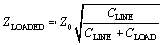
In the present case study the line velocity v is assumed equal to 1.4410 8 m/s, and the overall length x equals 25 cm, for a total line delay of x / v = 1.73 ns. The total line capacitance is (1.73 ns/50 W ) = 34.6 pF. To that amount the loads have added 15 more pF, bringing the total to 49.6. The square root of 34.6/49.6, multiplied times the original raw trace impedance of 50 W , reveals an actual loaded impedance of 41.7 W . If that is the true impedance of the structure, why not try a 40- W end termination? The results of this experiment appear in Figure 12.50.
Figure 12.50. Changing the termination to better match the loaded impedance of the structure (not just the impedance of the raw transmission line) eliminates overshoot.
The waveforms in Figure 12.50 look clean and usable. They are particularly impressive given that the signal is daisy-chained across five loads. You'll get the same good daisy-chain performance if you follow these three rules:
- Uniformly space the loads,
- With a spacing whose delay is small compared to the signal rise and fall time, and
- Terminate the structure with a resistance that matches the effective impedance of the loaded structure you've built, not just the impedance of the raw trace you started with.
What if your timing budget can't afford a slower driver, or if no such driver is available in your logic (or ASIC) family? In this case you must do something to iron out the bumps in the signal pathway. One obvious improvement would be to reduce the spacing between the taps. The shorter the spacing, the faster a rise or fall time you can use. Unfortunately, this approach has the disadvantage of spreading the same total load capacitance across a transmission line of lesser total length, thereby more severely reducing the loaded impedance of the structure. Also, in many cases you may already have reduced the line to its bare minimum length, so that no further shrinkage may be possible. Have hope, dear reader, as all hope is not lost. Section 5.3.1.3, "Potholes," describes one approach that can partially compensate for the capacitive lumps in your highway . Check out Section 5.3.1.3 for the details of how to do the calculations; here I'll just show a couple of results.
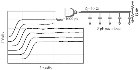
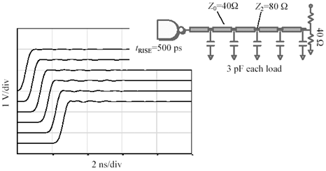
First, let's keep the 40- W end termination, but revert to a 500 ps driver (Figure 12.51). This signal displays the familiar lumpy pattern from Figure 12.48, but without the 10% overshoot. The last figure of this group (Figure 12.52) modifies the line widths to produce two new impedances of 40 W and 80 W . The 40- W segments form the main body of the structure. Wherever a load appears, it is bracketed by a short section of 80- W trace. The length of each 80- W section is 11.6 mm. The structure in Figure 12.52 supports rise and fall times twice as fast as the structure in Figure 12.50. The new structure can be reliably clocked at 500 MHz or even faster.
Figure 12.51. Leave the 40-ohm termination in place, but revert back to the 500-ps driver.
Figure 12.52. Modulate the trace width to partially compensate for the excess capacitance at each load.
POINT TO REMEMBER
- Rules for good daisy-chainingUniformly space the loads, with a spacing whose delay is small compared to the signal rise and fall time, and terminate the structure with a resistance that matches the effective impedance of the loaded structure you've built, not just the impedance of the raw trace you started with.
Fundamentals
- Impedance of Linear, Time-Invariant, Lumped-Element Circuits
- Power Ratios
- Rules of Scaling
- The Concept of Resonance
- Extra for Experts: Maximal Linear System Response to a Digital Input
Transmission Line Parameters
- Transmission Line Parameters
- Telegraphers Equations
- Derivation of Telegraphers Equations
- Ideal Transmission Line
- DC Resistance
- DC Conductance
- Skin Effect
- Skin-Effect Inductance
- Modeling Internal Impedance
- Concentric-Ring Skin-Effect Model
- Proximity Effect
- Surface Roughness
- Dielectric Effects
- Impedance in Series with the Return Path
- Slow-Wave Mode On-Chip
Performance Regions
- Performance Regions
- Signal Propagation Model
- Hierarchy of Regions
- Necessary Mathematics: Input Impedance and Transfer Function
- Lumped-Element Region
- RC Region
- LC Region (Constant-Loss Region)
- Skin-Effect Region
- Dielectric Loss Region
- Waveguide Dispersion Region
- Summary of Breakpoints Between Regions
- Equivalence Principle for Transmission Media
- Scaling Copper Transmission Media
- Scaling Multimode Fiber-Optic Cables
- Linear Equalization: Long Backplane Trace Example
- Adaptive Equalization: Accelerant Networks Transceiver
Frequency-Domain Modeling
- Frequency-Domain Modeling
- Going Nonlinear
- Approximations to the Fourier Transform
- Discrete Time Mapping
- Other Limitations of the FFT
- Normalizing the Output of an FFT Routine
- Useful Fourier Transform-Pairs
- Effect of Inadequate Sampling Rate
- Implementation of Frequency-Domain Simulation
- Embellishments
- Checking the Output of Your FFT Routine
Pcb (printed-circuit board) Traces
- Pcb (printed-circuit board) Traces
- Pcb Signal Propagation
- Limits to Attainable Distance
- Pcb Noise and Interference
- Pcb Connectors
- Modeling Vias
- The Future of On-Chip Interconnections
Differential Signaling
- Differential Signaling
- Single-Ended Circuits
- Two-Wire Circuits
- Differential Signaling
- Differential and Common-Mode Voltages and Currents
- Differential and Common-Mode Velocity
- Common-Mode Balance
- Common-Mode Range
- Differential to Common-Mode Conversion
- Differential Impedance
- Pcb Configurations
- Pcb Applications
- Intercabinet Applications
- LVDS Signaling
Generic Building-Cabling Standards
- Generic Building-Cabling Standards
- Generic Cabling Architecture
- SNR Budgeting
- Glossary of Cabling Terms
- Preferred Cable Combinations
- FAQ: Building-Cabling Practices
- Crossover Wiring
- Plenum-Rated Cables
- Laying Cables in an Uncooled Attic Space
- FAQ: Older Cable Types
100-Ohm Balanced Twisted-Pair Cabling
- 100-Ohm Balanced Twisted-Pair Cabling
- UTP Signal Propagation
- UTP Transmission Example: 10BASE-T
- UTP Noise and Interference
- UTP Connectors
- Issues with Screening
- Category-3 UTP at Elevated Temperature
150-Ohm STP-A Cabling
- 150-Ohm STP-A Cabling
- 150- W STP-A Signal Propagation
- 150- W STP-A Noise and Interference
- 150- W STP-A: Skew
- 150- W STP-A: Radiation and Safety
- 150- W STP-A: Comparison with UTP
- 150- W STP-A Connectors
Coaxial Cabling
- Coaxial Cabling
- Coaxial Signal Propagation
- Coaxial Cable Noise and Interference
- Coaxial Cable Connectors
Fiber-Optic Cabling
- Fiber-Optic Cabling
- Making Glass Fiber
- Finished Core Specifications
- Cabling the Fiber
- Wavelengths of Operation
- Multimode Glass Fiber-Optic Cabling
- Single-Mode Fiber-Optic Cabling
Clock Distribution
- Clock Distribution
- Extra Fries, Please
- Arithmetic of Clock Skew
- Clock Repeaters
- Stripline vs. Microstrip Delay
- Importance of Terminating Clock Lines
- Effect of Clock Receiver Thresholds
- Effect of Split Termination
- Intentional Delay Adjustments
- Driving Multiple Loads with Source Termination
- Daisy-Chain Clock Distribution
- The Jitters
- Power Supply Filtering for Clock Sources, Repeaters, and PLL Circuits
- Intentional Clock Modulation
- Reduced-Voltage Signaling
- Controlling Crosstalk on Clock Lines
- Reducing Emissions
Time-Domain Simulation Tools and Methods
- Ringing in a New Era
- Signal Integrity Simulation Process
- The Underlying Simulation Engine
- IBIS (I/O Buffer Information Specification)
- IBIS: History and Future Direction
- IBIS: Issues with Interpolation
- IBIS: Issues with SSO Noise
- Nature of EMC Work
- Power and Ground Resonance
Points to Remember
Appendix A. Building a Signal Integrity Department
Appendix B. Calculation of Loss Slope
Appendix C. Two-Port Analysis
- Appendix C. Two-Port Analysis
- Simple Cases Involving Transmission Lines
- Fully Configured Transmission Line
- Complicated Configurations
Appendix D. Accuracy of Pi Model
Appendix E. erf( )
Notes
EAN: N/A
Pages: 163
- Key #1: Delight Your Customers with Speed and Quality
- Key #4: Base Decisions on Data and Facts
- Making Improvements That Last: An Illustrated Guide to DMAIC and the Lean Six Sigma Toolkit
- The Experience of Making Improvements: What Its Like to Work on Lean Six Sigma Projects
- Six Things Managers Must Do: How to Support Lean Six Sigma
