Pcb Applications
The following sections describe the main applications for differential signaling on pcbs.
6.11.1 Matching to an External, Balanced Differential Transmission Medium
Differential traces are often used to connect to balanced cabling. For this purpose, the tightness of coupling between the two traces making up the differential pair is irrelevant. What matters is that the differential characteristic impedance of trace configuration matches the differential characteristic impedance of the balanced cabling.
The most popular types of balanced cabling are 100- W twisted-pair cabling (ISO 11801 categories 3, 5, 5e, 6, and 7), and the old 150- W shielded twisted-pair cabling (IBM Type I). When connecting directly to these cabling types, one normally uses two 50-ohm traces (or two 75-ohm traces for 150- W cabling) to couple into the cable.
Figure 6.21 depicts a typical LAN coupling situation. The target cable is a 100- W unshielded twisted-pair cable. Your objective in this application is to generate a purely differential transmitted signal of standard size with as little high-frequency power and as low a common-mode content as practicable.
Figure 6.21. Ethernet 10/100BASE-T interface, showing use of 50- W transmission lines to match 100- W balanced load.
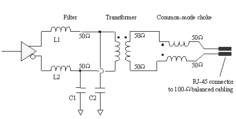
The low-pass filter formed by L1-C1 (and L2-C2) truncates any unnecessary power in the frequency range above the bandwidth of the digital signal. The natural balance of the transformer combined with the additional balancing properties of the common-mode choke together serve to limit the common-mode content of the transmitted waveform. The reason common-mode balance is so important is that common-mode radiation from an unshielded twisted-pair cable is many orders of magnitude more efficient than differential-mode radiation. Minimizing the common-mode current minimizes the cable emissions.
After passing through the common-mode choke you should make the two pcb traces as symmetrical as possible, with equal impedances to ground. The traces must be symmetrically positioned with respect to all nearby grounded objects, but they do not necessarily need to be tightly coupled to each other.
POINTS TO REMEMBER
- Match the differential characteristic impedance of two pcb traces to the differential characteristic impedance of a balanced cable.
- Make the two pcb traces as symmetrical as possible, with equal impedances to ground.
6.11.2 Defeating Ground Bounce
Differential signals arrive naturally at a receiver with a built-in reference voltage. The receiver of a differential signal need not rely on its own internal reference, which could be corrupted by ground bounce or other disturbances in the reference supply. Differential signaling defeats ground bounce.
For ground-bounce cancellation to work, the receiver must see two complementary signals with equal delays from the driver. Any ground shifts or disturbances along the way that affect both wires equally will be cancelled at the receiver.
Note that the two halves of a differential signal must arrive synchronously so that they will be equally influenced by noise, but they do not necessarily need to be tightly coupled to each other.
POINT TO REMEMBER
- Differential signaling defeats ground bounce.
6.11.3 Reducing EMI with Differential Signaling
Differential signals radiate less than single-ended signals. That's one of the benefits of differential logic. If the two complementary signals of a differential pair are perfectly balanced, the degree of field cancellation is determined entirely by the separation between traces.
If, however, the two complementary signals are not perfectly balanced, then the degree of attainable field cancellation will be limited to a minimum value determined not by the trace spacing, but by the common-mode balance of the differential pair. Because the common-mode balance of most digital drivers is not particularly good, it often happens that differential pairs radiate far more power in the common-mode than in the differential mode. In such a situation no radiation benefit remains to be gained from squeezing the differential traces more closely together.
Figure 6.22 plots the theoretical radiation gain attained by a differential microstrip pair as a function of trace separation. The figure assumes the measurement antenna is located in the plane of the board, removed in a broadside direction a distance r = 10 m away from the traces (worst case). The radiation from one trace of the differential pair is supposed to be cancelled by the equal and opposite radiation from the adjacent trace, resulting in a marked reduction in emissions. The depth of cancellation is related to the ratio 2 p s / l , where l is the free-space wavelength of the highest frequency of interest and s is the separation between traces. This ratio controls the relative phase relationship of the two near-complementary waves as they leave your board. The cancellation is also related to the ratio r /( r + s ), which speaks to the relative intensities of the two near-complementary waves as they reach the antenna. The formula in Figure 6.22 shows that differential cancellation improves as you reduce s .
Figure 6.22. Theoretical radiation improvement a for the differential portion of the far-field radiation from a microstrip, as a function of trace separation s .
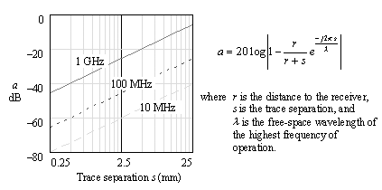
The common-mode radiation from the two traces of a differential microstrip reinforces rather than cancels, so that common-mode radiation does not vary strongly with trace separation. You can adjust the differential-mode radiation by adjusting the trace spacing, but you can't do much about the common-mode radiation (except to install a driver with better common-mode balance).
Under FCC class B measurement conditions, the differential-mode radiation from a differential microstrip pair with 0.5-mm (0.020-in.) separation should theoretically yield a 40-dB radiation improvement at 1 GHz, compared to the radiation measured if the same signal were implemented as a single ended layout. Smaller separations should yield even more improvement. While that theory sounds appealing, in practice you will rarely if ever achieve as much as a 40-dB improvement in overall radiation because your gains will be limited by the degree of balance available on the two outputs of your differential transmitter. Unless the outputs are balanced to better than 1 part in 100, a common-mode radiation component of at least 1% of the differential amplitude will emanate from your differential pair anyway. Given a 1% common-mode imbalance, even a differential spacing of zero would not improve the total radiation by more than 40 dB.
Taking an example from the LVDS differential driver family, which prescribes a differential balance no better than 1 part in 16, even the most Herculean efforts at trace balancing will never improve the overall radiation for that logic family by more than a factor of 16 (24 dB).
In plain terms, a differential trace spacing of 0.5 mm is close enough to deliver all the EMI benefit you are likely to ever achieve. Because radiation problems on digital pcbs are usually dominated by the common-mode radiation, you need not struggle to place ordinary differential digital traces any closer than 0.5 mm for any EMI purpose.
POINT TO REMEMBER
- You need not struggle to place ordinary differential digital traces any closer than 0.5 mm (0.020 in.) for any EMI purpose.
6.11.4 Punching Through a Noisy Connector
When two systems are mated by a connector, the net flow of signal current between the systems returns to its source through the ground (or power) pins of the connector. As it does so, tiny voltages are induced across the inductance of the connector's ground (or power) pins. These tiny voltages appear as a difference between the ground (or power) voltage on one side of the connector and the ground (or power) voltage on the other side. This problem is called a ground shift , and it is yet another form of common impedance coupling. In a single-ended communications system the ground shift voltages detract directly from the available noise margin for your logic family. In a differential signaling system, the ground-shift voltages don't matter, because they affect both wires of the differential pair equally. Subject to the limits of common-mode rejection , ground shifts generated within a connector are totally cancelled within the receiver.
Differential signaling usually reduces crosstalk generated by either mutual inductance or mutual capacitance within the connector itself. The exact gains available depend on the relative spacing of the differential signals as they pass through the connector and the distance to the nearest aggressive source. If the aggressive source is closer to one element of the pair, the crosstalk will not affect both pairs equally, and it will therefore not be cancelled in the receiver.
The cancellation of ground shifts generated by a connector and the cancellation of nearby aggressors within a connector both have a lot to do with the position of the signal pins within the connector, but very little to do with the pcb trace layout, or intertrace coupling.
POINT TO REMEMBER
- Subject to the limits of common-mode rejection, ground shifts generated within a connector are totally cancelled within a differential receiver.
6.11.4.1 Differential Signaling (Through Connectors)
[52] Connectors with solid ground shields between columns of pins are usually designed to accommodate differential pairs collocated within each shielded cavity . This implies that the pin lengths may differ for the two elements of each pair. A perfect differential shielded connector would be designed to match the skew on each element of a differential pair as it traverses the connector, even if the elements were located on different rows. If your connector produces a known skew, it's up to you to cancel it somewhere else in the layout.
6.11.5 Reducing Clock Skew
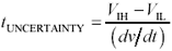
When a digital component receives a clock, the precise moment at which the clock is recognized depends upon the switching threshold for that component. For 5-V TTL logic, the switching threshold is defined to be somewhere between 0.8V ( V IL ) and 2.4V ( V IH ). The spread between V IL and V IH defines a window shown in Figure 6.23 within which the actual clock transition takes place:
Equation 6.25
|
where |
t UNCERTAINTY is the uncertainty (skew) in the clock switching moment, |
|
V IH and V IL are the worst-case guaranteed high and low logic thresholds respectively, and |
|
|
dv / dt is the rate of change of voltage on the clock input ( roughly equal to the logic swing D V divided by the 10% to 90% risetime of the driver). [53] |
[53] The risetime emanating from an unreasonably fast driver will be modified by the package parasitics of the receiver. The risetime of the signal measured at the input pads of the receiver die is therefore generally not quite as fast as the risetime measured external to the package. It is the risetime of the internal signal combined with the receiver switching thresholds that determines the actual amount of switching uncertainty. If the driver and receiver are implemented in similar technology, and the package is not deemed a significant impediment to reception , you may simply use the driver risetime for the calculation of dv/dt in equation [6.25].
Figure 6.23. The input thresholds and the risetime of the input signal combine to create an uncertainty in the precise switching time for a clock.
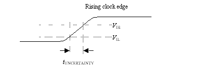
The smaller you can make this uncertainty, the less clock skew you will have to recognize in your timing budget. In the differential world a similar effect takes place, but the specifications for V IH and V OL are replaced by a specification for the offset voltage of the receiver. The input offset voltage is the differential input voltage at which a particular receiver actually switches. An ideal receiver would switch precisely at zero (when the inputs are equal), regardless of common-mode voltage, temperature, power supply quality, age, and so on. Such a part would have an input offset voltage of zero. Practical receivers always switch at some finite, hopefully small, value. There is no way to predict the polarity of the offset. [54] The spec sheet for a differential receiver usually provides a worst-case upper bound for the magnitude of the offset. The effective spread between V IH and V IL for a differential receiver is twice the maximum offset magnitude.
[54] Unless the device is manufactured with a purposeful offset in one direction or another.
A relevant figure of merit for comparing differential logic families in this regard is the ratio of the spread in differential input offset voltage to the peak-to-peak differential output voltage swing. [55] For single-ended logic the corresponding figure of merit is the spread between V IH and V IL divided by the peak-to-peak output voltage swing. Differential logic usually fares better on this measure of performance.
[55] In a differential signaling architecture, the peak-to-peak differential output voltage swing is twice as large as the peak-to-peak voltage swing on either of the two inputs.
In a differential clock distribution system one usually attempts to match the delays of the two complementary signal traces as they traverse a pcb. The two traces need not follow the same path ; they just need to have the same delay. If the delays of the two traces are unequal , if affects the switching time. For example, suppose the two complementary halves of a differential signal arrive at successive times t 1 and t 2 . Let the separation between t 1 and t 2 be a small fraction (perhaps 1/10) of a rising edge. Under these conditions the receiver will switch very nearly at the average arrival time ( t 1 + t 2 )/2. In the worst case, if the separation is as great as a risetime, the receiver will switch no earlier than t 1 and no later than t 2 . I normally match the delay of the two traces in a differential signal to within 1/20 of the signal risetime.
The clock skew contributed by a clock receiver is a function of the input risetime, the switching thresholds, and, for differential signaling, the degree of similarity in the times of arrival of the two complementary signals. Clock skew has little or nothing to do with trace spacing or geometry (other than delay).
POINTS TO REMEMBER
- Differential receivers often have more accurately specified switching thresholds than single-ended receivers.
- Uncoupled differential traces need not follow the same path; they just need to have the same delay.
6.11.6 Reducing Local Crosstalk
Differential traces on a pcb do a relatively poor job of reducing local crosstalk. As illustrated in Figure 6.24, when some local aggressive trace approaches a differential pair, the interference is not balanced. Interference couples much more strongly to the near side of a differential pair than to the far side.
Figure 6.24. Differential signaling does not offer much help with nearby crosstalk.
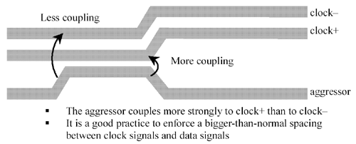
In the figure, clock+ is twice as close to the aggressor as clock “, so you get a 4:1 difference in the crosstalk coupled into the two sides. Imbalanced crosstalk of this sort cannot be cancelled by a differential receiver. The receiver sees almost the full value of crosstalk from the aggressive trace to the clock+, with little or no cancellation from clock “.
The best way to prevent crosstalk onto a differential pair is to design a keep-out zone around the sensitive traces, forcing other traces to stay at a respectable distance. All modern layout systems support separation rules by net class that will allow you to keep big, dirty signal traces away from delicate, sensitive ones.
Cramming the traces of a differential pair closer together does yield marginal improvements in crosstalk reduction, but you don't get the big benefit you get from simply moving the whole pair further away from the problem. Figure 6.25 provides data to support this assertion. The data for this plot were generated using a sheet- conductance measurement method [56] .
Figure 6.25. The crosstalk immunity of differential pairs is not much improved by tight coupling; mostly what matters is the interpair spacing.
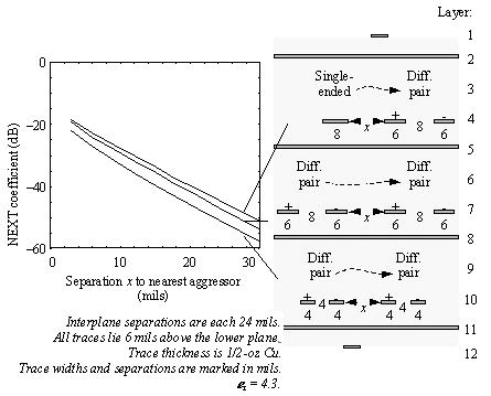
The figure plots crosstalk for three trace configurations. Each plot shows the measured near-end crosstalk coefficient in dB versus the separation x between traces. [56]
[56] Measurements performed using salt-water tank per Howard Johnson, "Rainy-Day Fun," EDN Magazine , March 4, 1999. This data has been corroborated against a commercial 2-D field solver.
The first scenario shows how a single-ended aggressor affects a differential pair. The next two scenarios show how two differential pairs affect each other. The difference between scenarios II and III is that the intrapair separation changes from 8 to 4 mils. In all cases the separation between planes is 24 mil, and the height of all traces above the nearest plane is 6 mil. The widths of all traces have been adjusted to give a characteristic impedance of 100 ohms for all differential transmission-line pairs and 50 ohms for the single-ended aggressor.
In all cases the crosstalk falls off steeply as you increase the separation x between the aggressor and victim. Looking at the difference between scenarios I and II, the addition of a complementary signal to the aggressor (changing it into a differential pair) tends to cancel a little bit of the interference, but the complementary signal is too far away to have much of an effect. The net reduction in interference is less than 2 dB. When you go from scenario II to III, reducing the intrapair separation, the complementary signals is brought into play. This reduces crosstalk by an additional 4 dB, which is useful, but still nowhere near as significant as simply moving the aggressor further away.
Tightly coupling a differential pair delivers only a modest improvement in crosstalk, and therefore only a modest improvement in the achievable pair pitch (see also Section 6.10.2, "Edge-Coupled Stripline ").
POINT TO REMEMBER
- Tightly coupling a differential pair delivers only a modest improvement in crosstalk.
6.11.7 A Good Reference about Transmission Lines
The Transmission Line Design Handbook by Brian C. Wadell [58] compiles handy approximations for transmission-line impedance, delay, skin effect loss, dielectric losses, and radiation losses. It is very comprehensive. The book addresses most of the popular transmission-line formats in use today, including microstrip, buried microstrip, offset stripline, and edge- or broadside-coupled differential striplines.
Wadell heavily references the original research articles and measurements. He doesn't pull any punches when the research is fuzzy or contradictory. He shows you just what is known and indicates what is not known. If you're looking for closed-form approximations, this is the best source.
P.S.: If you have an old copy of Wadell's text, check out his errata list on the Web.
6.11.8 Differential Clocks
POINT TO REMEMBER
- The benefits of differential signaling apply to multidrop configurations.
6.11.9 Differential Termination
POINT TO REMEMBER
- Every long, differential link needs at least one good differential termination and also a reasonable common-mode termination to prevent severe common-mode resonance.
6.11.10 Differential U- Turn
POINT TO REMEMBER
- Visualize the propagation of a differential signal as a quad of four currents.
6.11.11 Your Layout Is Skewed
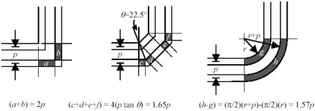
 6.4 ps to a low of 1.57 p
 POINT TO REMEMBER
- Chamfering or rounding of differential corners does not eliminate skew.
6.11.12 Buying Time
POINT TO REMEMBER
- A pair that starts and ends going north has by definition equal numbers of right-hand and left-hand turns.
Fundamentals
- Impedance of Linear, Time-Invariant, Lumped-Element Circuits
- Power Ratios
- Rules of Scaling
- The Concept of Resonance
- Extra for Experts: Maximal Linear System Response to a Digital Input
Transmission Line Parameters
- Transmission Line Parameters
- Telegraphers Equations
- Derivation of Telegraphers Equations
- Ideal Transmission Line
- DC Resistance
- DC Conductance
- Skin Effect
- Skin-Effect Inductance
- Modeling Internal Impedance
- Concentric-Ring Skin-Effect Model
- Proximity Effect
- Surface Roughness
- Dielectric Effects
- Impedance in Series with the Return Path
- Slow-Wave Mode On-Chip
Performance Regions
- Performance Regions
- Signal Propagation Model
- Hierarchy of Regions
- Necessary Mathematics: Input Impedance and Transfer Function
- Lumped-Element Region
- RC Region
- LC Region (Constant-Loss Region)
- Skin-Effect Region
- Dielectric Loss Region
- Waveguide Dispersion Region
- Summary of Breakpoints Between Regions
- Equivalence Principle for Transmission Media
- Scaling Copper Transmission Media
- Scaling Multimode Fiber-Optic Cables
- Linear Equalization: Long Backplane Trace Example
- Adaptive Equalization: Accelerant Networks Transceiver
Frequency-Domain Modeling
- Frequency-Domain Modeling
- Going Nonlinear
- Approximations to the Fourier Transform
- Discrete Time Mapping
- Other Limitations of the FFT
- Normalizing the Output of an FFT Routine
- Useful Fourier Transform-Pairs
- Effect of Inadequate Sampling Rate
- Implementation of Frequency-Domain Simulation
- Embellishments
- Checking the Output of Your FFT Routine
Pcb (printed-circuit board) Traces
- Pcb (printed-circuit board) Traces
- Pcb Signal Propagation
- Limits to Attainable Distance
- Pcb Noise and Interference
- Pcb Connectors
- Modeling Vias
- The Future of On-Chip Interconnections
Differential Signaling
- Differential Signaling
- Single-Ended Circuits
- Two-Wire Circuits
- Differential Signaling
- Differential and Common-Mode Voltages and Currents
- Differential and Common-Mode Velocity
- Common-Mode Balance
- Common-Mode Range
- Differential to Common-Mode Conversion
- Differential Impedance
- Pcb Configurations
- Pcb Applications
- Intercabinet Applications
- LVDS Signaling
Generic Building-Cabling Standards
- Generic Building-Cabling Standards
- Generic Cabling Architecture
- SNR Budgeting
- Glossary of Cabling Terms
- Preferred Cable Combinations
- FAQ: Building-Cabling Practices
- Crossover Wiring
- Plenum-Rated Cables
- Laying Cables in an Uncooled Attic Space
- FAQ: Older Cable Types
100-Ohm Balanced Twisted-Pair Cabling
- 100-Ohm Balanced Twisted-Pair Cabling
- UTP Signal Propagation
- UTP Transmission Example: 10BASE-T
- UTP Noise and Interference
- UTP Connectors
- Issues with Screening
- Category-3 UTP at Elevated Temperature
150-Ohm STP-A Cabling
- 150-Ohm STP-A Cabling
- 150- W STP-A Signal Propagation
- 150- W STP-A Noise and Interference
- 150- W STP-A: Skew
- 150- W STP-A: Radiation and Safety
- 150- W STP-A: Comparison with UTP
- 150- W STP-A Connectors
Coaxial Cabling
- Coaxial Cabling
- Coaxial Signal Propagation
- Coaxial Cable Noise and Interference
- Coaxial Cable Connectors
Fiber-Optic Cabling
- Fiber-Optic Cabling
- Making Glass Fiber
- Finished Core Specifications
- Cabling the Fiber
- Wavelengths of Operation
- Multimode Glass Fiber-Optic Cabling
- Single-Mode Fiber-Optic Cabling
Clock Distribution
- Clock Distribution
- Extra Fries, Please
- Arithmetic of Clock Skew
- Clock Repeaters
- Stripline vs. Microstrip Delay
- Importance of Terminating Clock Lines
- Effect of Clock Receiver Thresholds
- Effect of Split Termination
- Intentional Delay Adjustments
- Driving Multiple Loads with Source Termination
- Daisy-Chain Clock Distribution
- The Jitters
- Power Supply Filtering for Clock Sources, Repeaters, and PLL Circuits
- Intentional Clock Modulation
- Reduced-Voltage Signaling
- Controlling Crosstalk on Clock Lines
- Reducing Emissions
Time-Domain Simulation Tools and Methods
- Ringing in a New Era
- Signal Integrity Simulation Process
- The Underlying Simulation Engine
- IBIS (I/O Buffer Information Specification)
- IBIS: History and Future Direction
- IBIS: Issues with Interpolation
- IBIS: Issues with SSO Noise
- Nature of EMC Work
- Power and Ground Resonance
Points to Remember
Appendix A. Building a Signal Integrity Department
Appendix B. Calculation of Loss Slope
Appendix C. Two-Port Analysis
- Appendix C. Two-Port Analysis
- Simple Cases Involving Transmission Lines
- Fully Configured Transmission Line
- Complicated Configurations
Appendix D. Accuracy of Pi Model
Appendix E. erf( )
Notes
EAN: N/A
Pages: 163
- An Emerging Strategy for E-Business IT Governance
- Assessing Business-IT Alignment Maturity
- Linking the IT Balanced Scorecard to the Business Objectives at a Major Canadian Financial Group
- Measuring and Managing E-Business Initiatives Through the Balanced Scorecard
- Governance in IT Outsourcing Partnerships
