Slow-Wave Mode On-Chip
The term slow-wave mode applies exclusively to on-chip interconnections implemented in a metal-insulator-semiconductor (MIS) configuration. On such interconnections the substrate resistance adds substantially to the signal loss and can sometimes have the peculiar effect of greatly slowing signal propagation. The resulting slow-wave mode occurs when the substrate conductivity is adjusted so that electromagnetic fields only partially penetrate the substrate. The wave velocity then becomes a function of the substrate, not just the good dielectric insulation between the trace and the top layer of the substrate.
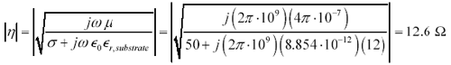
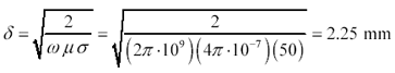
Figure 2.32 illustrates a classic on-chip MIS transmission line, comprising a metal trace, a 1- m m silicon dioxide insulating layer, and a 200- m m semiconducting substrate. The solid metal layer on the back of the substrate is called backside metallization . In this example I'll assume a worst-case value for the conductivity of the silicon substrate layer, about 50 S/m. At a frequency of 1 GHz, the intrinsic impedance h and skin depth d of the substrate are
Equation 2.106
Equation 2.107
|
where |
|
|
m is the magnetic permeability (H/m), and |
|
|
s is the conductivity (S/m) of the substrate. |
|
|
For nonmagnetic substrate materials, m = 4 p ·10 “7 H/m. |
|

Figure 2.32. Metal-insulator-semiconductor (MIS) transmission lines suffer from the limited conductivity of the substrate.
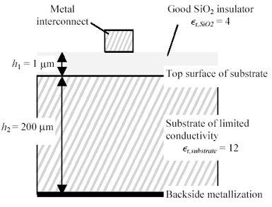
At 1 GHz the low intrinsic impedance of the substrate (12.6 ohms) prevents electric fields from penetrating . The transmission line therefore inherits a large amount of capacitance in accordance with the small distance h 1 between the trace and the top of the substrate.
Magnetic fields behave differently. At 1 GHz the penetration of magnetic fields (skin depth) greatly exceeds the thickness h 2 of the substrate, so the magnetic fields and their associated returning signal currents permeate the entire semiconducting substrate layer. The complete penetration of magnetic fields creates a large amount of inductance in accordance with the relatively large distance h 2 between the trace and the bottom of the substrate.
The difficulty with this circuit is that the electric and magnetic fields have become separated. In a perfect, homogeneous dielectric material, where the electric and magnetic fields both penetrate to the same depth, the velocity of propagation always equals  .
.
In this slow-wave example, the electric fields penetrate to a depth of h 1 , while the magnetic fields penetrate all the way down to h 2 , disconnecting the homogeneous assumption. The resulting combination of large capacitance and large inductance creates an absurdly slow velocity of signal propagation, much slower than would be indicated by the permittivity of either the insulator or the substrate acting alone.
In Figure 2.32 the velocity of propagation for a 1-GHz sine wave approaches 1/5 the speed of light in air. Furthermore, the complicated frequency dependencies associated with the slow-wave effect create significant phase distortion in the received waveform.
The slow-wave effect has been reported by numerous authors [16] , [17] , [18] . The consensus view about how to fix the problem is quite clear. You have three choices:
- Raise the substrate conductivity by doping until it acts like a good, low-impedance return path . This approach shrinks the skin depth, forcing currents to flow mostly near the top surface of the semiconducting substrate. The line delay then depends only on the permittivity of the insulator (about 4.0 for silicon dioxide).
- Decrease the substrate conductivity (by doping) until it acts like a good, high-impedance insulator. The electric and magnetic fields then completely penetrate the substrate layer together. The line delay in this case then depends mostly on the permittivity of the substrate (about 12.0 for lightly doped silicon). A high-speed chip requires backside metallization for this approach to work.
- Add intentional metallic return paths near the signal traces.
In the world of pcb design, the dielectric materials have such a low conductivity that one almost always adopts the configuration of solution 2. This approach implies the existence of a solid-metal reference plane somewhere in the layer stack. The reference plane serves the same purpose in a pcb as the backside metallization in a chip ”it defines a good return-current path for all signals.
Occasionally, a board designer will implement solution 3. For example, in a 100BASE-TX interface, for the connection between the isolation transformer and the RJ-45 plug, you might use a co-planar differential pair with no underlying reference plane. The differential pair comprises a signal trace and an associated return-current conductor, so it meets the definition of solution 3.
In no case do pcb designers worry about the slow-wave mode or the implications of solution 1, because pcbs never use crummy, partly conducting substrates. That's one of the nice benefits of working at the printed-circuit design level.
The only way to separate the electric and magnetic fields on a pcb is to implement a nonuniform trace. For example, attaching hundreds of little cross-bars (like cilia) to a pcb trace adds a substantial amount of capacitance without changing the inductance, creating an absurdly low impedance and high delay.
POINT TO REMEMBER
- In an on-chip MIS configuration, if the electric fields penetrate to a depth of h 1 , while the magnetic fields penetrate to a futher depth h 2 , the resulting combination of large capacitance and large inductance creates an absurdly slow velocity of signal propagation.
For further study see: www.sigcon.com
Fundamentals
- Impedance of Linear, Time-Invariant, Lumped-Element Circuits
- Power Ratios
- Rules of Scaling
- The Concept of Resonance
- Extra for Experts: Maximal Linear System Response to a Digital Input
Transmission Line Parameters
- Transmission Line Parameters
- Telegraphers Equations
- Derivation of Telegraphers Equations
- Ideal Transmission Line
- DC Resistance
- DC Conductance
- Skin Effect
- Skin-Effect Inductance
- Modeling Internal Impedance
- Concentric-Ring Skin-Effect Model
- Proximity Effect
- Surface Roughness
- Dielectric Effects
- Impedance in Series with the Return Path
- Slow-Wave Mode On-Chip
Performance Regions
- Performance Regions
- Signal Propagation Model
- Hierarchy of Regions
- Necessary Mathematics: Input Impedance and Transfer Function
- Lumped-Element Region
- RC Region
- LC Region (Constant-Loss Region)
- Skin-Effect Region
- Dielectric Loss Region
- Waveguide Dispersion Region
- Summary of Breakpoints Between Regions
- Equivalence Principle for Transmission Media
- Scaling Copper Transmission Media
- Scaling Multimode Fiber-Optic Cables
- Linear Equalization: Long Backplane Trace Example
- Adaptive Equalization: Accelerant Networks Transceiver
Frequency-Domain Modeling
- Frequency-Domain Modeling
- Going Nonlinear
- Approximations to the Fourier Transform
- Discrete Time Mapping
- Other Limitations of the FFT
- Normalizing the Output of an FFT Routine
- Useful Fourier Transform-Pairs
- Effect of Inadequate Sampling Rate
- Implementation of Frequency-Domain Simulation
- Embellishments
- Checking the Output of Your FFT Routine
Pcb (printed-circuit board) Traces
- Pcb (printed-circuit board) Traces
- Pcb Signal Propagation
- Limits to Attainable Distance
- Pcb Noise and Interference
- Pcb Connectors
- Modeling Vias
- The Future of On-Chip Interconnections
Differential Signaling
- Differential Signaling
- Single-Ended Circuits
- Two-Wire Circuits
- Differential Signaling
- Differential and Common-Mode Voltages and Currents
- Differential and Common-Mode Velocity
- Common-Mode Balance
- Common-Mode Range
- Differential to Common-Mode Conversion
- Differential Impedance
- Pcb Configurations
- Pcb Applications
- Intercabinet Applications
- LVDS Signaling
Generic Building-Cabling Standards
- Generic Building-Cabling Standards
- Generic Cabling Architecture
- SNR Budgeting
- Glossary of Cabling Terms
- Preferred Cable Combinations
- FAQ: Building-Cabling Practices
- Crossover Wiring
- Plenum-Rated Cables
- Laying Cables in an Uncooled Attic Space
- FAQ: Older Cable Types
100-Ohm Balanced Twisted-Pair Cabling
- 100-Ohm Balanced Twisted-Pair Cabling
- UTP Signal Propagation
- UTP Transmission Example: 10BASE-T
- UTP Noise and Interference
- UTP Connectors
- Issues with Screening
- Category-3 UTP at Elevated Temperature
150-Ohm STP-A Cabling
- 150-Ohm STP-A Cabling
- 150- W STP-A Signal Propagation
- 150- W STP-A Noise and Interference
- 150- W STP-A: Skew
- 150- W STP-A: Radiation and Safety
- 150- W STP-A: Comparison with UTP
- 150- W STP-A Connectors
Coaxial Cabling
- Coaxial Cabling
- Coaxial Signal Propagation
- Coaxial Cable Noise and Interference
- Coaxial Cable Connectors
Fiber-Optic Cabling
- Fiber-Optic Cabling
- Making Glass Fiber
- Finished Core Specifications
- Cabling the Fiber
- Wavelengths of Operation
- Multimode Glass Fiber-Optic Cabling
- Single-Mode Fiber-Optic Cabling
Clock Distribution
- Clock Distribution
- Extra Fries, Please
- Arithmetic of Clock Skew
- Clock Repeaters
- Stripline vs. Microstrip Delay
- Importance of Terminating Clock Lines
- Effect of Clock Receiver Thresholds
- Effect of Split Termination
- Intentional Delay Adjustments
- Driving Multiple Loads with Source Termination
- Daisy-Chain Clock Distribution
- The Jitters
- Power Supply Filtering for Clock Sources, Repeaters, and PLL Circuits
- Intentional Clock Modulation
- Reduced-Voltage Signaling
- Controlling Crosstalk on Clock Lines
- Reducing Emissions
Time-Domain Simulation Tools and Methods
- Ringing in a New Era
- Signal Integrity Simulation Process
- The Underlying Simulation Engine
- IBIS (I/O Buffer Information Specification)
- IBIS: History and Future Direction
- IBIS: Issues with Interpolation
- IBIS: Issues with SSO Noise
- Nature of EMC Work
- Power and Ground Resonance
Points to Remember
Appendix A. Building a Signal Integrity Department
Appendix B. Calculation of Loss Slope
Appendix C. Two-Port Analysis
- Appendix C. Two-Port Analysis
- Simple Cases Involving Transmission Lines
- Fully Configured Transmission Line
- Complicated Configurations
Appendix D. Accuracy of Pi Model
Appendix E. erf( )
Notes
EAN: N/A
Pages: 163
- The Effects of an Enterprise Resource Planning System (ERP) Implementation on Job Characteristics – A Study using the Hackman and Oldham Job Characteristics Model
- Context Management of ERP Processes in Virtual Communities
- Data Mining for Business Process Reengineering
- Healthcare Information: From Administrative to Practice Databases
- Development of Interactive Web Sites to Enhance Police/Community Relations
