CMOS Image Sensors
Another image sensor technology has joined the market in the past years : image sensors which are structured like a CMOS [5] memory chip and therefore need row and column address decoders. These sensors make use of a photon-to- electron -to-voltage conversion, taking place in each pixel element.
[5] Complementary metal oxide semiconductor: an MOS technology that makes use of complementary (n- and p-channel) transistor types.
Figure 2.20 shows the principle of such CMOS image sensors , which leads to a number of advantages, as well as to some drawbacks. The main advantages are the following:
Figure 2.20. Principle of a CMOS Image Sensor
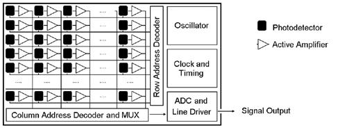
- It is possible to access not only the entire picture, but also a single picture element and a number of pixels, a region of interest (ROI), which is also needed in the image processing and analysis sections. An ROI can be defined by addressing the row and column address decoders.
- Some additional system components , like clocking and timing, can be integrated on the same chip with the image sensor. This makes the camera cheaper and more reliable.
- CMOS chips have natural blooming and image smear immunity.
Another main difference is the description of the image speed; CCD sensors are described in terms of images per second or frames per second , which is not useful with CMOS sensors if you consider the single pixel or the ROI access. Here, we are talking about the pixel clock ; for example, a pixel clock of 5 MHz will lead to about 65 frames per second if the image frame is 320 x 240 pixels.
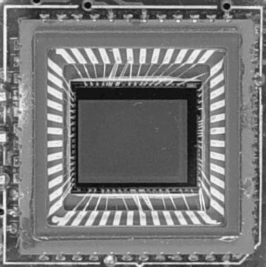
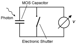
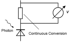
Table 2.1 compares some properties of CMOS image sensors with those of CCDs. The first line (technology) explains how the photocurrent, which is generated by the light radiation on the pixel, is transferred in the related voltage. In CCD sensors, this is done after the electron charge, generated in an MOS capacitor , is transferred to the sensor output. In CMOS sensors, each pixel element has an integrated active amplifier , which generates the voltage and can be accessed by the row and column address decoders. Figure 2.21 shows a CMOS sensor chip; on the right and on the bottom of the sensor the address decoder areas are visible.
Figure 2.21. CMOS (Color) Sensor Chip
A great disadvantage of CMOS image sensors is their noise generation. The continuous conversion of the photocurrent in the circuit shown in Table 2.1, adds an additional noise source to the signal generation. The main reason is that the CMOS production process is not primarily designed for photoelements, resulting in a poorer sensitivity. Thus, the necessary higher amplification leads to a significantly higher noise level. Moreover, as in CCD sensors, fixed pattern noise (FPN) is another main issue.
Table 2.1. Comparison of CCD and CMOS Technology
|
CCD |
CMOS |
|
|---|---|---|
|
Technology: |
|
|
|
Pixel access: |
only full image |
single pixel possible |
|
Power: |
relatively high |
low power consumption |
|
Integration: |
only sensor on chip |
more functions on chip possible |
|
Conversion: |
after charge transfer (full image) |
at each pixel |
|
Noise: |
FPN, statistical |
additional noise sources |
|
Blooming: |
antiblooming techniques |
natural blooming immunity |
|
Smear: |
caused by charge transfer |
no image smear possible (Figure 2.23) |
Because of the construction of CMOS image sensors, they show absolute immunity from blooming or image smear. Blooming ”the "overflow" of a high amount of electrons in one cell into the neighbor cells ”cannot occur in CMOS sensors, because the electron-to-voltage transfer already takes place in the cell itself. Figure 2.22 shows again the blooming effect in a CCD image sensor (Figure 2.11; the sensor itself can be seen in Figure 2.15), compared to the behavior of a CMOS sensor (Figure 2.21).
Figure 2.22. Blooming Effect in CCD (left) and CMOS Cameras (right)
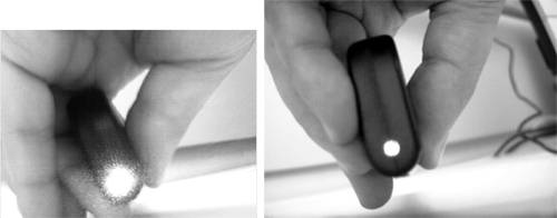
Figure 2.23 shows the behavior difference between CCD und CMOS regarding image smear sensitivity. Recall that image smear is the vertical transportation of "errors" during the image readout process. In this example, the sensor area (without lens) is illuminated with a laser pointer, thus flooding the respective sensor areas with photons . The left image, the CCD sensor response, shows a significant smear effect; the area beneath the illumination spot is lighted as well.
Figure 2.23. Smear Effect in CCD (left) and CMOS Cameras (right)
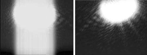
The right image shows the behavior of a CMOS sensor with the same laser pointer illumination. Here, the illumination spot is clearly limited, showing absolutely no image smear effect.
You can find more in-depth information about CMOS image sensors, for example, in [17] and [18].
Video Standards |
Introduction and Definitions
- Introduction
- Some Definitions
- Introduction to IMAQ Vision Builder
- NI Vision Builder for Automated Inspection
Image Acquisition
- Image Acquisition
- Charge-Coupled Devices
- Line-Scan Cameras
- CMOS Image Sensors
- Video Standards
- Color Images
- Other Image Sources
Image Distribution
- Image Distribution
- Frame Grabbing
- Camera Interfaces and Protocols
- Compression Techniques
- Image Standards
- Digital Imaging and Communication in Medicine (DICOM)
Image Processing
Image Analysis
- Image Analysis
- Pixel Value Analysis
- Quantitative Analysis
- Shape Matching
- Pattern Matching
- Reading Instrument Displays
- Character Recognition
- Image Focus Quality
- Application Examples
About the CD-ROM
EAN: 2147483647
Pages: 55
