Charge-Coupled Devices
If you consider the matrix structure of an image we discussed in the previous chapter, you might ask yourself the following questions:
- What should be the look of a sensor that can acquire images of the previously defined matrix type?
- How is the data transferred between the sensor and the display? [1]
[1] This is a very general expression; I will simply use "computer" or "PC" in the future.
The answer to question 1 seems easy: in general, the sensor will have the same structure as the image itself: the structure of a rectangular matrix, which obviously seems to be the optimal solution. We talk about another possible answer to this question later in this chapter.
Figure 2.1. Questions Regarding Pixel Transfer
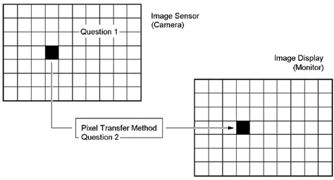
The second question is more difficult to answer; obviously, it is not possible to connect each pixel to the respective area on the pixel display, in most cases, a computer monitor. In this book, we often use image sizes of 320 x 240 pixels; a direct connection would require 320 · 240 = 76,800 cables between sensor and PC. Therefore, in the first step, the sensor data has to be collected, transferred over cables or other media following a data protocol that is always somehow serial, and finally rearranged for display on a monitor (see Figure 2.1).
CCDs, or charge-coupled devices, are image sensors that already provide data preparation in the manner mentioned above. Imagine a sensor that consists of a number of photodetectors, one for each pixel. After these photodetectors have measured a certain brightness for the corresponding pixel, this value is shifted vertically into the next row below (see Figure 2.2).
Figure 2.2. Principle of a CCD Sensor
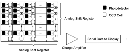
Of course, the brightness value cannot be shifted from one photodetector to another; we need other components for this operation. Therefore, each photodetector is connected to a MOS capacitor in combination with a transfer gate; Figure 2.2 shows these two elements as a CCD cell . Every time a new value set reaches the bottom row of the image sensor (here, the CCD cells do not have corresponding photodetectors), the values are shifted horizontally to the sensor output.
Principle of Functionality
MOS capacitors (MOS stands for metal oxide semiconductor) can store a number of electrons (described by the electrical charge Q ), which were previously generated by the corresponding photodetector, for a certain time. The electrical charge Q results from the photodetector current
Equation 2.1

with
|
I ph |
... |
photo(detector) current; |
|
S |
... |
light sensitivity, depending on the light wavelength; |
|
F e |
... |
light radiation power; |
and is therefore related to the brightness of the light in the respective sensor area.
Figure 2.3. CCD Transfer Mechanism [14]
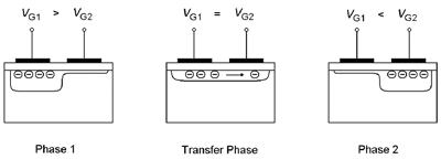
The transfer mechanism from one CCD cell to another is shown in Figure 2.3. If the voltage level V G1 at the gate of the MOS capacitor that contains the electrical charge Q is higher than the voltage level V G2 at the gate of the next MOS capacitor, the charge is kept in capacitor 1 (phase 1 or initial phase). If V G1 changes from High to Low and V G2 changes from Low to High, the electrons are transferred (in this figure) from left to right.
It is quite easy to imagine that if the system shown in Figure 2.3 is continued to the left and to the right, the transfer will not work in a specific direction; the electrons would be transferred to the right side and to the left side as well. Therefore, real CCD systems use more transfer phases to direct the electrons in a defined direction; in Figure 2.2, to the bottom of the sensor.
Unfortunately, some of the electrons are lost during the transfer process; this phenomenon is described by the charge transfer efficiency or CTE. This value defines the percentage of charge that is transmitted during a single transfer process; because of the accumulation of this value, CTE should be significantly higher than 99.99%.
Figure 2.4 shows the CTE for an array of MOS capacitors with a gate length of 4 m m, depending on the pulse length of the control signal; here, the pulse length should be at least 1.5 ns in order to guarantee a satisfactory CTE value.
Figure 2.4. Charge Transfer Efficiency (CTE) as a Function of Pulse Length [14]
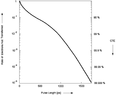
Figure 2.5. Impact of Charge Transfer Efficiency (CTE) on Pixel Brightness
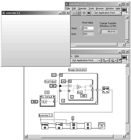
Exercise 2.1: Charge Transfer Efficiency.
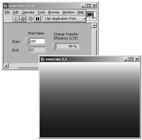
Create a LabVIEW VI that visualizes the impact of the charge transfer efficiency (CTE) on the brightness value of a 320 x 240 image. Figure 2.5 shows a possible solution, in which only the vertical influence of the CTE is taken into account. Change the value of CTE from 90% to 99.999% and watch the decrease of the pixel value in the lowest row, which should be 255. You can see in Figure 2.5 that a CTE value of 99.9% already causes a significant brightness decrease in the lower rows of the image. A CTE of 99%, as shown in Figure 2.6, makes the image unusable.
Figure 2.6. Charge Transfer Efficiency (CTE) Far Too Low
Surface Channel CCDs
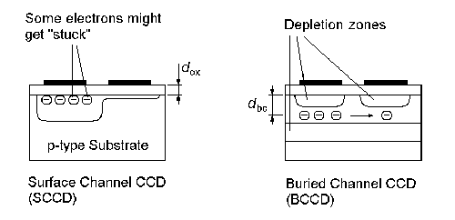
The configuration shown in Figure 2.3 is called surface channel CCD , or SCCD , because the electrons of the charge Q are kept on the surface of the semiconductor area. This leads to a significant disadvantage ; a number of electrons "stick" at the semiconductor-oxide junction and are not transferred to the next MOS capacitor. This number of electrons varies statistically and therefore leads to a noise signal, called transfer noise .
A possible solution would be not to empty the MOS capacitors completely during the transfer; the fixed electrons can remain on the junction and will not contribute to the transfer noise. Again, reality shows that this does not work in all areas of the capacitor, though the transfer current will decrease, but not disappear.
Figure 2.7. Structure of Surface Channel and Buried Channel CCDs
Buried Channel CCDs
Figure 2.7 shows the structure of a surface channel CCD (left) in comparison with a buried channel CCD (or BCCD; right). Here, a thin depletion zone is inserted at the Si-SiO 2 junction. The electron charge is therefore kept between the two depletion zones shown in the right half of Figure 2.7 and can be totally transferred to the next MOS capacitor because the Si-SiO 2 junction, which normally causes stuck electrons, is at a safe distance. This structure leads to a significantly lower transfer noise.
In an SCCD cell, the amount of charge that can be stored in the capacitor is given by the area-specific oxide capacitance C' ox , influenced only by the oxide thickness d ox and the dielectricity constant of the oxide  ox . In a BCCD, the electrons are kept at a distance d bc from the Si-SiO 2 junction, which will lead to a resulting capacitance
Equation 2.2

responsible for the amount of charge that can be stored in a BCCD. That this value is significantly lower than the maximum possible charge in an SCCD is one of the major drawbacks of BCCDs. The relation
Equation 2.3

describes the capacitance reduction in a BCCD, which can be up to 50%.
Another advantage of BCCDs is that the pulse frequency for the transfer process can be significantly higher; peristaltic CCDs (PCCDs) can be clocked with some 100 MHz [14].
Properties
Let us summarize topics we just discussed:
- CCDs or charge-coupled devices consist of at least a single shift register, in most cases of a combination of shift registers, which form a two-dimensional array for the use in image sensors.
- The CCD cells of these shift registers contain an amount of charge, which is related to the brightness [2] at the respective CCD cell and will later be represented by one pixel (picture element).
[2] This implies that the shift register is carrying analog information. In digital systems, we are working with shift registers with digital information, so CCDs are really an exception.
- The shift register concept enables easy parallel-serial conversion by shifting the values to the sensor bottom and reading out a single information line.
The following sections discuss the most relevant properties of CCDs that influence the image quality and therefore influence all image processing and analysis methods .
Sensitivity and Resolution
The spectral sensitivity of a CCD is in general determined by the photoelements. Various filter layers can be used to obtain a sensitivity maximum in different spectral regions ; this is the way color CCDs are realized: by three photoelements for each pixel and red, green, and blue color filters.
Infrared sensitivity can be obtained if Schottky photoelements are used in the CCD. They can detect wave lengths up to 5.7 m m and temperature differences down to 0.02 ° C [14]. Infrared sensitive cameras can be used, for example, in military or medical applications.
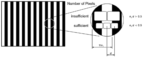
The resolution capability of a CCD can be described by the modulation transfer function , or MTF. It is defined as the modulation of the output signal if the CCD sensor looks at an image consisting of black and white stripes . If d is the distance between two sensor pixels and n s the number of black and white stripe pairs, the product d n s gives a measure for the resolution capability; if d n s << 1, the resolution of the black and white stripes is easy. For d n s > 0.5, it is not possible to distinguish between two neighboring lines. The function can be mathematically described by
Equation 2.4

It is easy to see that at least two sensor pixels are required to detect a black-and-white stripe pair (see Figure 2.8).
Figure 2.8. Visualization of the Modulation Transfer Function (MTF). How many pixels are needed to distinguish between a certain number of black and white lines?
The index 0 in Eq. (2.4) indicates that this function is theoretical. The real MTF is influenced by a number of other factors, such as the charge transfer efficiency CTE or light diffraction and dispersion.
Noise and "Hot Pixels"
The noise generated in a CCD is described by the signal-noise ratio SNR
Equation 2.5

with n signal as the number of electrons that contributes to the image signal and n noise as the number of "noise electrons"; noise can be divided into two main parts :
- The fixed pattern noise , FPN, which is caused by the physical differences of the single CCD cells. If all of the photoelements and CCD cells were identical, the FPN would be zero.
- The statistical noise , which can itself be divided into
- the photon noise , given by the square root of the number of signal electrons n signal ;
- the CCD noise , caused by electrons generated in the CCD cells; [3]
[3] To be exact, we would also have to count FPN as a part of the CCD noise.
- the amplifier noise , which is generated in the output amplifier.
A special kind of noise that occurs in almost every CCD camera is caused by hot pixels . They have their origins in small contaminations or production faults in the CCD sensor area and lead to a higher charge loss in the respective CCD cell during the exposure time. I took a picture with my own digital camera (Olympus CAMedia C-2000 Z), manual exposure time 1/2s, in a totally dark room and additionally closed the camera objective with my hand. You can find the image on the attached CD-ROM.
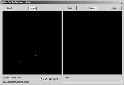
Figure 2.9 shows the locations of the detected hot pixels of my camera. One can reduce the hot pixel effect by averaging, not in the CCD chip itself, of course, but in the digital image. Some companies offer freeware tools for this procedure, for example, MediaChance (http://www.mediachance.com/digicam/hotpixels.htm).
Figure 2.9. Hot Pixels of a 2.1 Megapixel CCD Camera
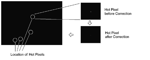
Figure 2.10 shows the processing window of the MediaChance Hot Pixel Eliminator with my hot pixel image loaded and processed .
Figure 2.10. MediaChance Hot Pixel Eliminator
Blooming
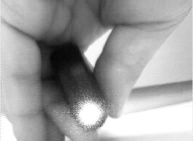
The blooming effect occurs especially in simple CCD image sensors and is caused by an overflow of electrons in the neighboring CCD cells. To the viewer, the result is an enlargement of the very light areas of the image. Figure 2.11 shows this effect by lighting the CCD chip with a laser pointer. The area of the light output is not as sharp as it should be, but the area (especially in the top) around the light output is frayed and shows enlarged light areas.
Figure 2.11. Blooming Effect Caused by a Laser Pointer
Modern CCDs have a number of mechanisms and techniques that should inhibit blooming:
- Antiblooming gates are located horizontally or vertically beside the CCD cells. If they are carrying the respective voltage, the electrons cannot be transferred in the neighbor cell but are caught by the antiblooming gate.
- Clocked antiblooming uses the natural recombination of electrons with "holes" in the semiconductor. The holes are generated by a specific clock structure and frequency.
We can add an exercise here, although it does not describe the blooming effect on a very technical level; it is just a simple LabVIEW exercise.
Figure 2.12. Blooming Effect (Exercise)
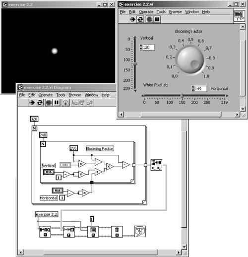
Exercise 2.2: Blooming Effect Simulation.
Create a VI that creates a single white pixel in a black image. The pixel can be moved by two numeric controls, one for the horizontal and one for the vertical position. Using another numeric control, you should be able to "influence" the surrounding pixels, depending on their distance from the white pixel (see Figure 2.12).
Image Smear
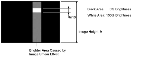
Smear is a fault signal that can be seen in the vertical neighborhood of a bright area in a dark image. It is generated by various causes, depending on the CCD technology and structure. Common to all causes is that the CCD cell content is changed during the transfer process.
Figure 2.13 shows a test image that is used for the measurement of the image smear effect. It consists of a white rectangle (100% brightness) of 10% height of the full image inside a totally black image (0% brightness). The resulting stripes above and below the white rectangle are caused by the image smear effect.
Figure 2.13. Test Image for Measuring the Smear Effect
Realization of CCD Devices
Until now we discussed only the theoretical aspects of CCD sensors. We did not talk about the practical realization, though sometimes we assumed that the most common application of CCD sensors are CCD cameras.
This section deals with some examples for practical realizations, starting with linear CCD sensors for measuring lengths or positions and then discussing the two main CCD structuring techniques: frame transfer configuration and interline configuration.
Linear CCD Sensors
In a linear CCD sensor , the CCD cells are arranged in a single line. The sensor can be used for measuring lengths or positions, with imaging the object to be measured by means of a lens on the linear sensor. The measurement itself is quite easy: simply count the sensor elements to an area of significant contrast change.
Usually, linear CCD sensors have two analog shift registers for odd and even pixels (see Figure 2.14). This leads to two big advantages [14]:
Figure 2.14. Structure of a Linear CCD Sensor
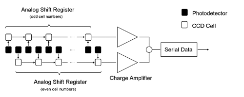
- The CCD clock frequency can be doubled without limiting the CTE.
- The size of the photoelements can only be half of the size of the shift register elements; this doubles the CCD's resolution.
It is also possible to use linear CCD sensors for image acquisition if the object of interest is moved relatively to the sensor. The best example of this technique is a fax machine; we talk about other applications using line-scan cameras later in this chapter.
Image Sensors
Recall the CCD principle we discussed in the beginning of this chapter, and especially Figure 2.2. This type of sensor, in which the charge is transferred horizontally from the photodetectors to the CCD cells and then vertically in the CCD cells from top to the bottom of the sensor, is called an interline transfer sensor .
This type of sensor is used for CCDs that allow short exposure times; [4] the major disadvantage of interline transfer sensors is that the light-sensitive area of each pixel is drastically reduced by the CCD capacitors, antiblooming gates, and so on. This effect is described by the fill factor , which specifies the fraction of the light-sensitive area to the total area.
[4] Do not confuse the term "exposure" in combination with a CCD sensor with the exposure mechanism of a mechanical camera. In general, a CCD uses a pixel-reset gate to control the exposure time; the same gate can be used to prevent horizontal blooming.
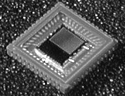
Figure 2.15 shows a CCD camera chip with interline structure; Figure 2.16 compares this structure with another possibility: the frame transfer sensor . Here, the sensor consists of two areas of approximately the same size (see right picture in Figure 2.16). The area at the top is light sensitive and captures the image information, which is then transferred to the shielded lower area, where the data is read out. Meanwhile, the sensitive area can capture the next image.
Figure 2.15. CCD Sensor Chip with Interline Structure
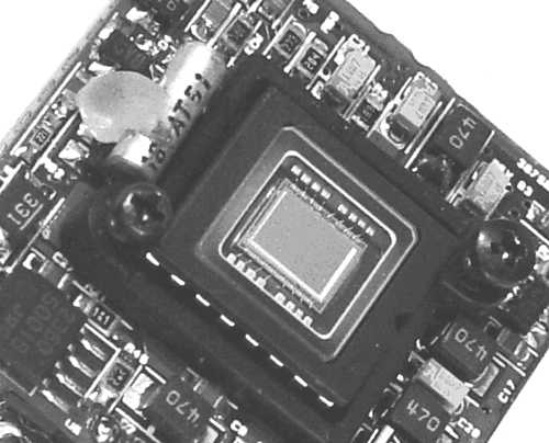
Figure 2.16. Comparison of Interline and Frame Transfer Structures
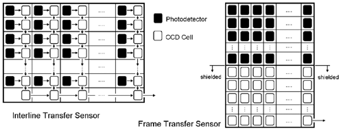
Because the shift registers of a frame transfer sensor are light sensitive themselves , the fill factor of this sensor is much higher than the fill factor of an interline sensor. Figure 2.17 shows a CCD chip with frame transfer structure.
Figure 2.17. CCD Sensor Chip with Frame Transfer Structure
Line Scan Cameras |
Introduction and Definitions
- Introduction
- Some Definitions
- Introduction to IMAQ Vision Builder
- NI Vision Builder for Automated Inspection
Image Acquisition
- Image Acquisition
- Charge-Coupled Devices
- Line-Scan Cameras
- CMOS Image Sensors
- Video Standards
- Color Images
- Other Image Sources
Image Distribution
- Image Distribution
- Frame Grabbing
- Camera Interfaces and Protocols
- Compression Techniques
- Image Standards
- Digital Imaging and Communication in Medicine (DICOM)
Image Processing
Image Analysis
- Image Analysis
- Pixel Value Analysis
- Quantitative Analysis
- Shape Matching
- Pattern Matching
- Reading Instrument Displays
- Character Recognition
- Image Focus Quality
- Application Examples
About the CD-ROM
EAN: 2147483647
Pages: 55
