Domain 4 Motherboard/Processors/Memory
Domain 4 Motherboard Processors Memory
CompTIA A+ Exam Objectives Covered in This Chapter
- 4.1 Distinguish between the popular CPU chips in terms of their basic characteristics.
- 4.2 Identify the types of RAM (Random Access Memory), form factors, and operational characteristics. Determine banking and speed requirements under given scenarios.
- 4.3 Identify the most popular types of motherboards, their components, and their architecture (bus structures).
- 4.4 Identify the purpose of CMOS (Complementary Metal-Oxide Semiconductor) memory, what it contains, and how and when to change its parameters. Given a scenario involving CMOS, choose the appropriate course of action.
Domain 4 of the exam covers the four major components of the processing subsystem: CPUs, RAM, motherboards, and CMOS. Whereas earlier objectives touched on these subjects in a general way (Domain 1, for example), or covered specifics about installing and troubleshooting them, this domain checks your knowledge of their technical specifications.
Distinguishing CPU Chips
Objective 4.1 ensures that you are familiar with the basic characteristics of a vast array of processors, beginning with the Pentium. Although it is helpful to study earlier CPUs for a complete understanding of how a CPU works in general, for study purposes you may confine your examination to Intel Pentium and higher CPUs and their competitors.
Critical Information
There are several ways of differentiating one CPU from another. The following sections explain specifications according to type, speed, voltage, and cache memory.
CPU Speed
The CPU’s speed is the frequency at which it executes instructions. This frequency is measured in millions of cycles per second, or megahertz (MHz); or billions of cycles per second, or gigahertz (GHz).
The CPU has an internal and an external speed. The external speed corresponds with the motherboard’s speed, based on its system crystal. The system crystal pulses, generating a cadence at which operations occur on the motherboard. Each pulse is called a clock tick. The CPU’s internal speed is usually a multiple of that, so that multiple operations occur internally per clock tick. A CPU’s speed as described in its specifications is its internal speed.
CPU Cache
Each CPU has at least two caches: L1 and L2. The L1 cache is built into the CPU on modern systems. It is the front-side cache, where data waits to enter the CPU. The L2 cache, or back-side cache, is where data exiting the CPU waits. On modern systems, the L2 cache is within the CPU’s packaging but not integrated into the CPU’s die. On older systems, the L2 cache was on a separate set of chips on the motherboard. You can compare one CPU to another according to the size of its L1 and L2 caches.
On some CPUs, the L2 cache operates at the same speed as the CPU itself; on others, the cache speed is only half the CPU speed. Chips with full-speed L2 caches have better performance.
Some newer systems also have an L3 cache, which is external to the CPU. It sits between the CPU and RAM to optimize data transfer between them.
CPU Voltage
A CPU’s voltage is the amount of electricity provided to it by the motherboard. Older CPUs have higher voltages (around +5V); newer ones have lower voltages (less than +2V in some cases).
One reason a given motherboard cannot support many different CPUs is that it must provide the correct voltage. To get around this issue, some motherboards have voltage regulator modules (VRMs) that are able to change the voltage based on the CPU.
CPU Manufacturers
The market leader in the manufacture of chips is Intel Corporation, with Advanced Micro Devices (AMD) gaining market share in the home PC market. Other competitors include Cyrix, Motorola, and IBM.
Intel Processors
The first commercially successful Intel CPU was the 8086, developed in the late 1970s. It was used in the IBM XT, one of the early home and business personal computers. Other early Intel CPUs included the 80286, 80386, and 80486. You might find it useful to learn about the specifications of these CPUs for your own knowledge, but they are not covered on the current A+ exam.
Pentium
Intel introduced the Pentium processor in 1993. This processor has 3.1 million transistors using a 64-bit data path, a 32-bit address bus, and a 16KB on-chip cache, and it comes in speeds from 60MHz to 200MHz. With the release of the Pentium chips, dual pipelining was introduced (also called superscalar architecture), allowing the chip to process two operations at once.
The term Pentium refers to three separate CPUs: first-generation, second-generation, and MMX. First-generation Pentiums were 273-pin PGA CPUs (Socket 4) drawing +5V. They ran at 60MHz or 66MHz. The second-generation Pentiums were 296-pin models (Socket 5 or Socket 7) drawing +3.3V. They ran at between 75Mhz and 200MHz.
Third-generation (MMX) Pentiums, released in 1997, added multimedia extensions (MMX) to help the CPU work with graphic-intensive games. They used Socket 7 sockets, drew +2.8V, and ran at 166MHz to 233MHz. Due to the voltage difference between the Pentium MMX CPU and other Socket 7 CPUs, the MMX CPU required a motherboard that either was specifically for that CPU or had a VRM that could take the voltage down to that level.
Pentium Pro
The Pentium Pro, released in 1995, came between the second- and third-generation Pentiums. Physically, the Pentium Pro was a PGA-style, rectangular chip with 387 pins, using a Socket 8 socket drawing +3V. It was designed primarily for server usage and was optimized for 32-bit operating systems. On a 16-bit OS like Windows 3.1, the Pentium Pro ran more slowly than a Pentium, so it failed to gain widespread consumer support.
The Pentium Pro included quad pipelining, which processed four operations at once. It was also the first CPU to include an on-chip L2 cache. Another advantage of the Pentium Pro was dynamic processing, which allowed it to run instructions out of order whenever it was waiting for something else to happen.
Pentium II
Intel next released the Pentium II: This chip’s speeds ranged from 233MHz to over 400MHz. It was introduced in 1997 and was designed to be a multimedia chip with special on-chip multimedia instructions and high-speed cache memory. It has 32KB of L1 cache, dynamic execution, and MMX technology. The Pentium II uses a Single Edge Connector Cartridge (SECC) to attach to the motherboard instead of the standard PGA package used with the earlier processor types.
When released, the Pentium II was designed for single-processor-only applications. Intel also released a separate processor, known as the Pentium II Xeon, to fill the need for multiprocessor applications such as servers. The Xeon’s primary advantage is a huge L2 cache (up to 2MB) that runs at the same speed as the CPU. The Xeon uses a special size of SECC-style slot called Slot 2.
Different voltages have been used for the Pentium II over its lifespan, ranging from +2.8V to +2.0V. When you’re using a Pentium II, it is important that the motherboard provide the correct voltage to it. This can be achieved with a VRM on the motherboard that detects the CPU’s needs and adjusts the voltage provided.
Celeron
To offer a less-costly alternative and to keep its large market share, Intel released the Celeron. In some cases, the Celeron was priced as low as half the retail price of the Pentium II. Because it was developed after the Pentium II, it benefited from some advancements and in certain aspects outperformed its more expensive counterpart. Intel has also named its low-budget Pentium III CPUs Celeron.
The Celeron CPU has come in several package types, including a 370-pin PGA socket (Socket 370) and a SECC variant called Single Edge Processor (SEP) that is similar to the circuit board inside an SECC cartridge but without the plastic outer shell.
Pentium III
The Pentium III was released in 1999 and uses the same SEC connector as its predecessor, the Pentium II. It included 70 new instructions and a processor serial number (PSN), a unique number electronically encoded into the processor. This number can be used to uniquely identify a system during Internet transactions.
The Pentium III has two styles: an SECC-style cartridge called SECC2, and a PGA-style chip with 370 pins. The Pentium III PGA chip has the CPU chip mounted on the top rather than the bottom of the ceramic square; it’s called a flip chip (FC), or FC-PGA.
| Note |
Like the Pentium II, the Pentium III has a multiprocessor Xeon version as well. |
Pentium 4
The Pentium 4 was released in 2002. It runs on a motherboard with a fast system bus (between 400MHz and 800MHz) and provides some incremental improvements over the Pentium III. It is a PGA-style CPU.
One of the improvements the Pentium 4 offers is hyperthreading technology. This feature that enables the computer to multitask more efficiently between CPU-demanding applications.
Summary of Intel Processors
Table 4.1 provides a summary of the history of the Intel processors. Table 4.2 shows the physical characteristics of Pentium (and higher) class processors.
|
Chip |
Year Added |
Data Bus Width (in Bits) |
Address Bus Width (in Bits) |
Speed (in MHz) |
|---|---|---|---|---|
|
8080 |
1974 |
8 |
8 |
2 |
|
8086 |
1978 |
16 |
20 |
5–10 |
|
8088 |
1979 |
8 |
20 |
4.77 |
|
80286 |
1982 |
16 |
24 |
8–12 |
|
386DX |
1985 |
32 |
32 |
16–33 |
|
386SX |
1988 |
32 |
24 |
16–20 |
|
486DX |
1989 |
32 |
32 |
25–50 |
|
486SX |
1991 |
32 |
32 |
16–33 |
|
487SX |
1991 |
32 |
32 |
16–33 |
|
486DX2 |
1991 |
32 |
32 |
33–66 |
|
486DX4 |
1992 |
32 |
32 |
75–100 |
|
Pentium |
1993 |
32 |
32 |
60–166 |
|
Pentium Pro |
1995 |
64 |
32 |
150–200 |
|
Pentium II |
1997 |
64 |
64 |
233–300 |
|
Pentium II Xeon |
1998 |
64 |
64 |
400–600 |
|
Celeron |
1999 |
64 |
64 |
400–600 |
|
Pentium III |
1999 |
64 |
64 |
350–1000 |
|
Pentium III Xeon |
1999 |
64 |
64 |
350–1000 |
|
Pentium 4 |
2002 |
64 |
64 |
1000–3000 |
|
Processor |
Speeds (MHz) |
Socket |
Pins |
Voltage |
|---|---|---|---|---|
|
Pentium-P5 (first generation) |
60–66 |
4 |
273 |
+5V |
|
Pentium-P54C (second generation) |
75–200 |
5 or 7 |
296 |
+3.3V |
|
Pentium-P55C (third generation) |
166–233 |
7 |
321 |
+2.8V |
|
Pentium Pro |
150–200 |
8 |
387 |
+3V |
|
Pentium II |
233–450 |
SECC |
N/A |
+2.0V–+2.8V |
|
Pentium III |
450–1130 |
SECC2 or Socket 370 |
370 |
+2.0V |
|
Pentium 4 |
1300–3000 (at this writing) |
Socket 423 or Socket 478 |
423 or 478 |
+1.53V–+1.75V |
Intel Clones and Others
Intel clones are processors that are based on the x86 architecture and are produced by other vendors; the most notable is AMD. AMD’s competitor to the Pentium II is the K6. The original K6 ran at between 166MHz and 300MHz. The K6-2, at 266MHz to 475MHz, added 3DNow! Technology, for improved multimedia. The K6-3, at 400MHz to 450MHz, adds a full-speed L2 cache. Because all the K6 chips are PGA, whereas Pentiums are SECC, you need a special motherboard for the K6 chips designed specifically for them.
AMD’s competitor to the Pentium III is the Athlon. It uses an SECC-style slot called Slot A that is physically the same but not pin-compatible with Intel-style Slot 1 SECC. AMD also has a low-budget version called the Duron that has less L2 cache.
| Tip |
The surest way to determine which CPU your computer is using is to open the case and view the numbers stamped on the CPU. Another way to determine a computer’s CPU is to save your work, exit any open programs, and restart the computer. Watch closely as the computer returns to its normal state. You should see a notation that tells you which chip you are using. If you are using MS-DOS, you can also run Microsoft Diagnostics to view the processor type (that is, unless your computer has a Pentium processor, in which case it will report a very fast 486). |
Exam Essentials
Understand the processor’s job.The processor is the brain of the PC. Most actions performed by the PC require use of the processor to accomplish their task.
Understand the differences between the different classes of Pentium chips.The Intel Pentium has gone through several changes since its release. You will need to understand the differences between the various classes in terms of their physical packaging, speeds, voltages, and caches.
Know what a VRM is.A voltage regulator module (VRM) on a motherboard allows it to change the voltage that it provides to the CPU to accommodate a wider range of CPUs.
Identifying the Types of RAM
To pass the A+ exam and be a productive computer technician, you must be familiar with memory. Not only will you be tested on this subject, but one of the most common upgrades performed on a PC is adding memory. Adding memory is a simple task, but before you can add memory you must have the correct type.
Critical Information
When we say memory, we are most often referring to Random Access Memory (RAM). However, there are other types of memory. We will discuss them all in this section. Be familiar with the various types and their usage.
Physical Memory
Physically, memory is a collection of integrated circuits that store data and program information as patterns of 1s and 0s (on and off states) in the chip. Most memory chips require constant power (also called a constant refresh) to maintain those patterns of 1s and 0s. If power is lost, all those tiny switches revert back to the off position, effectively erasing the data from memory. Some memory types, however, do not require a refresh.
There are many types of Random Access Memory (RAM). In this section, we examine each type in detail.
SRAM
Static RAM (SRAM) stores whatever is placed in it until it is changed. Unlike Dynamic RAM, it does not require constant electrical refreshing. Another name for it is Non-Volatile RAM (NVRAM). It is expensive, so it is not typically used for the main memory in a system.
DRAM
Dynamic RAM (DRAM) is an improvement over SRAM. DRAM uses a different approach to storing the 1s and 0s. Instead of using transistors, DRAM stores information as charges in very small capacitors. If a charge exists in a capacitor, it’s interpreted as a 1. The absence of a charge is interpreted as a 0.
Because DRAM uses capacitors instead of switches, it needs to use a constant refresh signal to keep the information in memory. DRAM requires more power than SRAM for refresh signals and, therefore, is mostly found in desktop computers.
DRAM technology allows several memory units, called cells, to be packed to a high density. Therefore, these chips can hold very large amounts of information. Most PCs today use DRAM of one type or another.
Let’s take a brief look at some of the different types of DRAM:
Fast Page Mode (FPM)An older type of RAM (almost always 72-pin SIMM packaging) that is not synchronized in speed with the motherboard. It is rated in nanoseconds of delay, with lower numbers being better (for example, 60ns). FPM is now obsolete.
Extended Data Out (EDO)Like FPM, an older type of RAM, usually in 72-pin SIMM form. It performs a bit better than normal FPM RAM because it needs to be refreshed less frequently. Like FPM, it is now obsolete.
Synchronous DRAM (SDRAM)Synchronized to the speed of the motherboard’s system bus. Synchronizing the speed of the systems prevents the address bus from having to wait for the memory because of different clock speeds. SDRAM typically comes in the form of 168-pin DIMMs or 184-pin RIMMs.
Double Data Rate (DDR) SDRAMEssentially, clock-doubled SDRAM. The memory chip can perform reads and writes on both sides of any clock cycle (the up, or start, and the down, or ending), thus doubling the effective memory executions per second. So, if you are using DDR SDRAM with a 100MHz memory bus, the memory will execute reads and writes at 200MHz and transfer the data to the processor at 100MHz. The advantage of DDR over regular SDRAM is increased throughput, and thus increased overall system speed.
Direct RambusA relatively new and extremely fast (up to 800MHz) technology that uses, for the most part, a new methodology in memory system design. Direct Rambus is a memory bus that transfers data at 800MHz. Direct Rambus memory models (often called Rambus Inline Memory Modules [RIMMs]), like DDR SDRAM, can transfer data on both the rising and falling edges of a clock cycle. That feature, combined with the 16-bit bus for efficient transfer of data, results in the ultra-high memory transfer rate (800MHz) and the high bandwidth of up to 1.6GBps.
Memory Chip Package Types
The memory chips themselves come in many different types of packages. The ones most frequently encountered are discussed in the following sections.
Dual Inline Package (DIP)
Dual Inline Package (DIP) memory is so named because the individual RAM chips use the DIP-style package for the memory module. Older computers, such as the IBM AT, arranged these small chips like rows of caskets in a small memory “graveyard.” This type of memory has long been obsolete.
SIMMs
Single Inline Memory Modules (SIMMs) were developed because DIPs took up too much real estate on the logic board. Someone got the idea to put several DIP chips on a small circuit board and then make that board easily removable.
Each of these RAM circuit boards is a stick of RAM. There are two sizes of SIMMs: 30-pin and 72-pin. The 30-pin are older, 8-bit sticks. The 72-pin are 32-bit sticks. Figure 4.1 shows one of each. SIMMs are called single because they are single sided. When you count the number of pins (the metal tabs) along the bottom, there are 30 or 72 of them. In contrast, DIMMs (Dual Inline Memory Modules) are double-sided; for example, a 168-pin DIMM has 84 pins on each side.
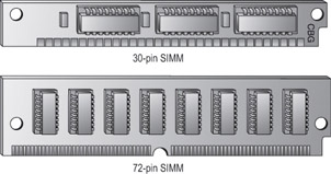
Figure 4.1: Single Inline Memory Modules (SIMMs)
DIMMs and RIMMs
Dual Inline Memory Modules (DIMMs) are double-sided memory chips used in modern systems (Pentium and higher). They typically have 168 pins and are 64 bits in width. Figure 4.2 shows a DIMM.
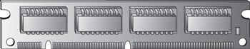
Figure 4.2: Dual Inline Memory Module (DIMM)
A RIMM is just like a DIMM, except it’s a Rambus DRAM stick, has 184 pins, and is slightly longer in size.
SoDIMMs and MicroDIMMs
Portable computers (notebooks and subnotebooks) require smaller sticks of RAM because of their smaller size. Two types are Small Outline DIMM (SoDIMM) and MicroDIMM.
Parity and Non-Parity RAM
Some sticks of RAM have a parity bit on them for error correction. It works by adding up the number of 1s in a particular row of data in RAM (for example, 32-bit RAM has 32 individual binary digits). It then adds either 1 or 0 to that total to make it come out even. When retrieving the data from RAM, it re-adds the 1s again, and if the parity bit doesn’t come out the same, it knows an error has occurred.
You can identify a parity SIMM by counting the number of chips on the stick. If there are nine, it’s parity RAM. If there are eight, it’s non-parity.
When do you choose parity RAM? Usually the motherboard requires either parity or non-parity; a few motherboards will accept either. Nowadays parity RAM is rarely needed because advances in RAM technology have created reliable RAM that seldom makes errors.
One type of parity RAM is ECC (Error Correction Code). This is a now-obsolete type of parity RAM. Most RAM today is non-ECC.
RAM Banks and Bit Width
As explained earlier, 30-pin SIMMs are 8-bit, 72-pin SIMMs are 32-bit, and DIMMs are 64-bit. The motherboard has an address bus that carries data from the RAM to the CPU and chipset. It has a certain width. On Pentium and higher systems, it’s 64-bit; on earlier systems it’s 32-bit (386 and 486) or less (286 and below). A bank of RAM is a single stick or a group of sticks where the collective bit width adds up to the width of the address bus.
For example, on a Pentium motherboard, a single bank consists of a single 64-bit DIMM or a pair of two 32-bit SIMMs. For a 486 motherboard, a single bank is a single 32-bit SIMM or four 8-bit SIMMs.
Video RAM
Video memory (also called Video RAM [VRAM]) is used to store image data for processing by the video adapter. The more video memory an adapter has, the better the quality of image that it can display. Also, more VRAM allows the adapter to display a higher resolution of image.
Exam Essentials
Know the differences among RAM types.Make sure you can differentiate among all the acronyms, such as SRAM, DRAM, SDRAM, DDR SDRAM, EDO DRAM, and so on.
Understand the different RAM packaging.Be able to differentiate between SIMMs and DIMMs, including the number of pins each has and their bit widths.
Know the purpose of parity in RAM.Understand how a parity bit is used for error correction.
Identifying Types of Motherboards
The motherboards is the backbone of a computer. The components of the motherboard provide basic services needed for the machine to operate and provide a platform for devices such as the processor, memory, disk drives, and expansion devices.
Critical Information
For this objective, you should study the types of motherboards, their ports and memory, the types of CPU sockets, and the types of expansion slots.
System Board Form Factors
Form factor refers to the size and shape of a component. There are three popular motherboard form factors for desktop PCs: AT, ATX, and NLX.
AT
AT is an older style of motherboard. A slightly more modern variant of it is the baby AT, which is similar but smaller. Its key features are a two-piece power supply connector, ribbon cables that connect the I/O ports to the board, and an AT-style keyboard connector. The expansion slots are parallel to the wide edge of the board. See Figure 4.3.
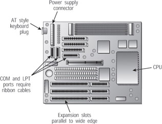
Figure 4.3: An AT-style motherboard
ATX
Most system boards today use the ATX form factor. It contains many design improvements over the AT, including I/O ports built directly into the side of the motherboard, the CPU positioned such that the power supply fan helps cool it, and allowing the PC to be turned on and off via software. It uses a PS/2 style connector for the keyboard. The expansion slots are parallel to the narrow edge of the board. See Figure 4.4.
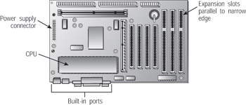
Figure 4.4: An ATX-style motherboard
NLX
This form factor is used in low-profile case types. This design incorporates expansion slots that are placed on a riser board to accommodate the reduction in case size. However, this design adds another component to troubleshoot.
Buses
A bus is a set of signal pathways that allows information and signals to travel between components inside or outside a computer. A motherboard has several buses, each with its own speed and width.
The external data bus, also called the system bus, connects the CPU to the chipset. On modern systems it is 64-bit. The address bus connects the RAM to the CPU. On modern systems it is 64-bit.
The expansion bus connects the I/O ports and expansion slots to the chipset. There are usually several different expansion buses on a motherboard. Expansion buses can be broken into two broad categories: internal and external. Internal expansion buses include ISA, PCI, and AGP; they are for circuit boards. External expansion buses include serial, parallel, USB, FireWire, and infrared. The following sections explain some of the most common buses.
| Note |
There are many obsolete bus types, including VESA Local Bus (VLB), Microchannel Architecture (MCA), and Enhanced ISA (EISA). These are not on the A+ test. |
Industry Standard Architecture (ISA) Bus
This is a 16-bit bus (originally 8-bit on the oldest computers) that operates at 8MHz. Its slots are usually black. New motherboards might not have this type of slot, because the ISA bus is old technology and is being phased out.
Besides the slow speed and narrow width, another drawback of the ISA bus is that each ISA device requires separate system resources, including separate IRQs. In a heavily loaded system, this can cause an IRQ shortage. (PCI slots, in contrast, can share some resources.)
Peripheral Component Interconnect (PCI)
The PCI bus is a fast (33MHz), wide (32-bit or 64-bit) expansion bus that is the modern standard in motherboards today for general-purpose expansion devices. Its slots are typically white. PCI devices can share IRQs and other system resources with one another in some cases. All modern motherboards have at least three PCI slots. Figure 4.5 shows some PCI slots.
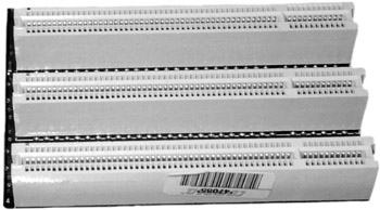
Figure 4.5: PCI bus connectors
Accelerated Graphics Port (AGP)
As systems got faster, PC game players wanted games that had better graphics, more realism, and more speed. However, as the computers got faster, the video technology couldn’t seem to keep up, even with the PCI bus. The Accelerated Graphics Port (AGP) bus was developed to meet this need.
The AGP slot is usually brown, and there is only one of them. It is a 32-bit or 64-bit bus, and it runs very fast (66MHz or faster). It is used exclusively for the video card. If you use a PCI video card, the AGP slot remains empty. See Figure 4.6.
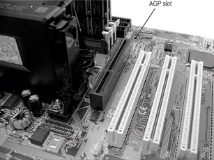
Figure 4.6: An AGP slot on a motherboard
Legacy Parallel and Serial
These buses are called legacy because they are old technology and are being phased out. The legacy serial port, also called an RS-232 port, is a 9-pin or 25-pin male connector. It sends data one bit at a time and is usually limited to about 115Kbps in speed.
The legacy parallel port transfers data 8 bits at a time. It is a 25-pin female connector. A system typically has only one parallel port, but because many printers are now coming with USB interfaces, this is no longer the inconvenience that it used to be.
Universal Serial Bus (USB)
Universal Serial Bus (USB) is a newer expansion bus type that is used almost exclusively for external devices. All motherboards today have at least two USB ports. Some of the advantages of USB include hot-plugging and the capability for up to 127 USB devices to share a single set of system resources. USB 1.1 runs at 12Mbps, and USB 2.0 runs at 480Mbps. Because USB is a serial interface, its width is 1 bit.
IEEE 1394/FireWire
Some newer motherboards have a built-in IEEE 1394/FireWire port, although this port is more typically found on a PCI expansion board. It transfers data at 400Mbps and supports up to 63 chained devices on a single set of resources. It is hot-pluggable, like USB.
Motherboard RAM Slots
RAM was discussed extensively under Objective 4.2; review that information to study the RAM portion of Objective 4.3. The RAM and the RAM slots on the motherboard must match.
Processor Sockets
Objective 4.1 covered CPUs; review that information here. In addition, review Table 4.3, which lists the various CPU slots and sockets you may find in a motherboard and explains which CPUs will fit into them.
|
Slot/Socket |
CPU Used |
|---|---|
|
Slot 1 |
Pentium II |
|
Slot 2 |
Pentium III |
|
Slot A |
AMD Athlon |
|
Socket A |
AMD Athlon |
|
Socket 7 |
Pentium (second and third generation), AMD K6 |
|
Socket 8 |
Pentium Pro |
|
Socket 423 |
Pentium 4 |
|
Socket 478 |
Pentium 4 |
|
Socket 370 |
Pentium III |
On-Motherboard Cache
On older motherboards, the L2 cache is on its own RAM-like stick made of very fast SRAM. It is known as cache on a stick (COAST). On newer systems, the L2 cache is built into the CPU packaging.
Some newer systems also have an L3 cache, which is an external cache on the motherboard that sits between the CPU and RAM.
IDE and SCSI On-Motherboard Interfaces
You studied IDE and SCSI interfaces in detail in Objectives 1.6 and 1.7; review that technical data about those buses with motherboards in mind. Most motherboards include two IDE channels but do not include built-in SCSI.
A consideration when choosing a motherboard for IDE is that it needs to support the desired level of UltraDMA to match the capabilities of the hard drive you want to use. Refer to Objective 1.6.
Chipsets
The chipset is the set of controller chips that monitors and directs the traffic on the motherboard between the buses. It usually consists of two or more chips. There are two basic chipset designs in motherboards: the north/south bridge chipset and the hub chipset.
North/south bridge is the older of the two. The north bridge c connects the system bus to the other relatively fast buses (AGP and PCI). The south bridge connects ISA, IDE, and USB. A third chip, SuperIO, connects the legacy parallel and serial ports.
The hub chipset includes a memory controller hub (equivalent to the north bridge), an I/O controller hub (equivalent to the south bridge), and a SuperIO chip.
Exam Essentials
Know the motherboard form factors.Understand the differences between AT, ATX, and NLX.
Distinguish among ISA, PCI, and AGP.Know their bus widths and maximum speeds, and that they’re all used for expansion boards inside the PC.
Distinguish among I/O ports on a motherboard.Know the different types of ports, such as USB, IEEE 1394, legacy parallel, and legacy serial.
Know the sizes and shapes of CPU slots/sockets.Be able to specify what type of socket or slot various CPUs require.
Understanding CMOS Memory
You can adjust a computer’s base-level settings through a BIOS Setup program, which you access by pressing a certain key at startup such as F1 or Delete (depending on the system). Another name for this setup program is CMOS Setup, which is what the A+ exam objectives call it. Objective 4.4 tests your familiarity with the settings in this utility and your ability to adjust them to solve certain problems.
Critical Information
The most common settings to adjust in CMOS include port settings (parallel, serial, USB), drive types, boot sequence, date and time, and virus/security protections.
Accessing CMOS Setup
Your PC keeps these settings in a special memory chip called the Complementary Metal Oxide Semiconductor (CMOS) chip. The CMOS chip must have a constant source of power to keep its settings. To prevent the loss of data, motherboard manufacturers include a small battery to power the CMOS memory. On modern systems this is a coin-style battery, about the same diameter of a dime and about 1/4-inch thick.
You can press a certain key or group of keys to access the setup program during the power on self-test (POST). This utility allows you to change the configuration through a group of menus. There are many different CMOS Setup programs, depending on the BIOS make and manufacturer, so it is impossible to provide specifics here; instead we will look at capabilities.
Load Setup Defaults
The purpose of this setting is to configure the PC back to the default settings set by the factory. If you make changes to your settings and the machine becomes disabled, in most cases selecting this menu item will return the machine to a usable state. You may then try different settings until you achieve your desired configuration. This is an important setting to know about before making any other changes.
Date and Time
One of the most basic things you can change in CMOS Setup is the system date and time. You can also change this from within the operating system.
CPU Settings
In most modern systems the BIOS detects the CPU’s type and speed automatically, so any CPU setting in CMOS Setup is likely to be read-only.
Memory Speed/Parity
Most systems today detect the RAM amount and speed automatically. Some motherboards can use different types of RAM, such as parity and non-parity, or different speeds, and the CMOS Setup program may provide the opportunity to change those settings. Increasingly, however, RAM is becoming a read-only part of CMOS Setup programs.
Power Management
The Power Management settings determine the way the PC will act after it has been idle for certain time periods. For example, you may have choices like Minimum, Maximum, and User Defined. The Minimum and Maximum settings control the HDD Off After, Doze Mode, Standby Mode, and Suspend Mode settings with predefined parameters. If you select User Defined, you must manually configure these settings to your personal preferences.
Ports and Peripherals
In CMOS Setup, you can enable or disable integrated components, such as built-in video cards, sound cards, or network cards. You might disable them in order to replace them with different models on expansion boards, for example.
You can also disable the on-board I/O ports for the motherboard, including parallel, serial, and USB. Depending on the utility, there may also be settings that enable or disable USB keyboard usage, Wake on LAN, or other special features.
In addition to enabling or disabling legacy parallel ports, you can also assign an operational mode to the port. Table 4.4 lists the common modes for a parallel port. When you’re troubleshooting parallel port problems, sometimes trying a different mode will help.
|
Setting |
Description |
Use |
|---|---|---|
|
EPP (Enhanced Parallel Port) |
Supports bidirectional communication and high transfer rates |
Newer inkjet and laser printers that can utilize bidirectional communication, and scanners |
|
ECP (Enhanced Communications Port) |
Supports bidirectional communication and high transfer rates |
Newer inkjet and laser printers that can utilize bidirectional communication, connectivity devices, and scanners |
|
SPP (Standard Printer Port) |
Supports bidirectional communication |
Older inkjet and laser printers and slower scanners |
Passwords
In most CMOS Setup programs, you can set a supervisor password. Doing so requires a password to be entered in order to use the CMOS Setup program, effectively locking out users from making changes to it. You may also be able to set a user password, which restricts the PC from booting unless the password is entered.
To reset a forgotten password, you can remove the CMOS battery to reset everything. There also may be a Reset jumper on the motherboard.
Virus Protection
Some CMOS Setup programs have a rudimentary virus-protection mechanism that prevents applications from writing to the boot sector of a disk without your permission. If this setting is turned on, and you install a new operating system, a confirmation box may appear at some point warning you that the operating system’s Setup program is trying to write to the boot sector. Let it.
HDD Auto Detection
Some CMOS Setup programs have a feature that polls the IDE channels and provides information about the IDE devices attached to them. You can use this feature to gather the settings for a hard disk. However, most hard disks these days are fully Plug and Play, so they automatically report themselves to the CMOS Setup.
Drive Configuration
You can specify how many floppy drives are installed and what types they are. Floppy drives are not automatically detected. The settings needed for a floppy drive are size (31/2-inch or 51/4-inch) and density (double-density or high-density). You can also set each floppy drive to be enabled or disabled from being bootable. Almost all floppy drives today are high-density 31/2-inch.
Hard drives, on the other hand, can be auto-detected by most systems if the IDE setting is set to Auto. The settings detected may include the drive’s capacity; its geometry (cylinders, heads, and sectors); and its preferred PIO, DMA, or UltraDMA operating mode. You can also configure a hard drive by entering its CHS values manually, but doing so is almost never necessary anymore.
| Note |
CHS stands for Cylinders, Heads, and Sectors. This is also called the drive geometry, as together these three numbers determine how much data the disk can hold. Most CMOS setup programs are able to automatically detect the CHS values. |
Boot Sequence
Each system has a default boot order, which is the order in which it checks the drives for a valid operating system to boot. Usually this order is set for floppy first, then hard disk, and finally CD-ROM, but these components can be placed in any boot order. For example, you might set CD-ROM first to boot from a Windows XP Setup disk on a system that already contained an operating system.
Exiting the CMOS Setup
The CMOS Setup program will include an Exit command, with options including Save Changes and Discard Changes. In most programs, Esc is a shortcut for exiting and discarding changes, and F10 is a common shortcut for exiting and saving changes.
Exam Essentials
Know what the CMOS Setup utility does.The CMOS Setup utility allows you to configure the characteristics of certain portions of the PC.
Be familiar with the common menu items listed.Knowing these common menu items and their function can greatly aid troubleshooting.
Understand the different printer port settings.Although there is no good rule of thumb on which of these settings will fix a communication error, in most cases you can resolve the issue by systematically trying the different settings.
Review Questions
|
1. |
On modern systems, what is the relationship between a CPU’s internal and external speeds? |
|
|
2. |
Which cache is also known as the back-side cache? |
|
|
3. |
What is the purpose of a VRM on a motherboard? |
|
|
4. |
What is the purpose of a parity bit on a SIMM? |
|
|
5. |
In a system with a 64-bit address bus, how many SDRAM DIMMs form a single bank of memory? |
|
|
6. |
What two essential system components are connected to one another via the address bus? |
|
|
7. |
Which type of expansion slot uses a 33MHz, 32-bit expansion bus and is the most common choice for general-purpose expansion in a modern system? |
|
|
8. |
What is the difference between USB 1.1 and USB 2.0? |
|
|
9. |
Besides Standard and Bidirectional, what are two parallel printer port modes you can choose in BIOS Setup? |
|
|
10. |
What chip holds the changes you make in BIOS Setup? |
|

Answers
|
1. |
The internal speed is a multiple of the external speed. |
|
2. |
The L2 cache |
|
3. |
To provide different voltages for different CPUs |
|
4. |
Error correction |
|
5. |
One |
|
6. |
The CPU and the RAM |
|
7. |
PCI |
|
8. |
Speed. USB 1.1 runs at 12Mbps, and USB 2.0 runs at 400 Mbps. |
|
9. |
EPP (Enhanced Parallel Port) and ECP (Enhanced Communications Port) |
|
10. |
CMOS |
Part I - A+: Core Hardware Service Technician Exam
- Domain 1 Installation, Configuration, and Upgrading
- Domain 2 Diagnosing and Troubleshooting
- Domain 3 Preventive Maintenance
- Domain 4 Motherboard/Processors/Memory
- Domain 5 Printers
- Domain 6 Basic Networking
Part II - A+ Operating System Technologies Exam
