Section 3.1. The Power Mac G5
3.1. The Power Mac G5Apple announced the Power Mac G5its first 64-bit desktop systemin June 2003. Initial G5-based Apple computers used IBM's PowerPC 970 processors. These were followed by systems based on the 970FX processor. In late 2005, Apple revamped the Power Mac line by moving to the dual-core 970MP processor. The 970, 970FX, and 970MP are all derived from the execution core of the POWER4 processor family, which was designed for IBM's high-end servers. G5 is Apple's marketing term for the 970 and its variants.
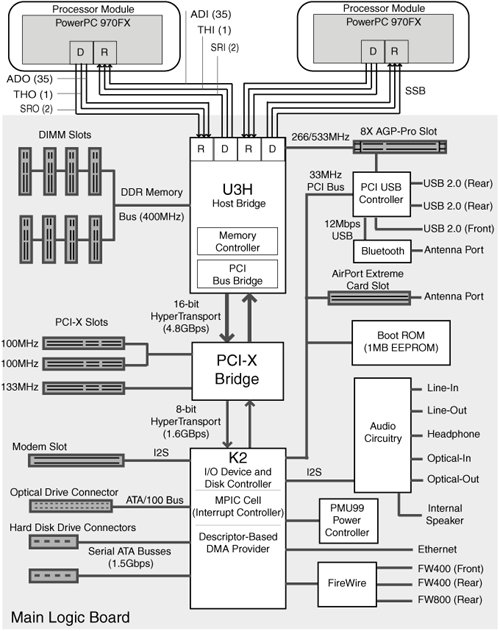
Before we examine the architecture of any particular Power Mac G5, note that various Power Mac G5 models may have slightly different system architectures. In the following discussion, we will refer to the system shown in Figure 31. Figure 31. Architecture of a dual-processor Power Mac G5 system 3.1.1. The U3H System ControllerThe U3H system controller combines the functionality of a memory controller[5] and a PCI bus bridge.[6] It is a custom integrated chip (IC) that is the meeting point of key system components: processors, the Double Data Rate (DDR) memory system, the Accelerated Graphics Port (AGP)[7] slot, and the HyperTransport bus that runs into a PCI-X bridge. The U3H provides bridging functionality by performing point-to-point routing between these components. It supports a Graphics Address Remapping Table (GART) that allows the AGP bridge to translate linear addresses used in AGP transactions into physical addresses. This improves the performance of direct memory access (DMA) transactions involving multiple pages that would typically be noncontiguous in virtual memory. Another table supported by the U3H is the Device Address Resolution Table (DART),[8] which translates linear addresses to physical addresses for devices attached to the HyperTransport bus. We will come across the DART in Chapter 10, when we discuss the I/O Kit.
3.1.2. The K2 I/O Device ControllerThe U3H is connected to a PCI-X bridge via a 16-bit HyperTransport bus. The PCI-X bridge is further connected to the K2 custom IC via an 8-bit HyperTransport bus. The K2 is a custom integrated I/O device controller. In particular, it provides disk and multiprocessor interrupt controller (MPIC) functionality. 3.1.3. PCI-X and PCI ExpressThe Power Mac system shown in Figure 31 provides three PCI-X 1.0 slots. Power Mac G5 systems with dual-core processors use PCI Express. 3.1.3.1. PCI-XPCI-X was developed to increase the bus speed and reduce the latency of PCI (see the sidebar "A Primer on Local Busses"). PCI-X 1.0 was based on the existing PCI architecture. In particular, it is also a shared bus. It solves manybut not allof the problems with PCI. For example, its split-transaction protocol improves bus bandwidth utilization, resulting in far greater throughput rates than PCI. It is fully backward compatible in that PCI-X cards can be used in Conventional PCI slots, and conversely, Conventional PCI cardsboth 33MHz and 66MHzcan be used in PCI-X slots. However, PCI-X is not electrically compatible with 5V-only cards or 5V-only slots. PCI-X 1.0 uses 64-bit slots. It provides two speed grades: PCI-X 66 (66MHz signaling speed, up to 533MBps peak throughput) and PCI-X 133 (133MHz signaling speed, up to 1GBps peak throughput). PCI-X 2.0 provides enhancements such as the following:
Note how the slots are connected to the PCI-X bridge in Figure 31: Whereas one of them is "individually" connected (a point-to-point load), the other two "share" a connection (a multidrop load). A PCI-X speed limitation is that its highest speed grades are supported only if the load is point-to-point. Specifically, two PCI-X 133 loads will each operate at a maximum of 100MHz.[9] Correspondingly, two of this Power Mac's slots are 100MHz each, whereas the third is a 133MHz slot.
The next revision of PCI-X3.0provides a 1066MHz data rate with a peak throughput of 8.5GBps. 3.1.3.2. PCI ExpressAn alternative to using a shared bus is to use point-to-point links to connect devices. PCI Express[10] uses a high-speed, point-to-point architecture. It provides PCI compatibility using established PCI driver programming models. Software-generated I/O requests are transported to I/O devices through a split-transaction, packet-based protocol. In other words, PCI Express essentially serializes and packetizes PCI. It supports multiple interconnect widthsa link's bandwidth can be linearly scaled by adding signal pairs to form lanes. There can be up to 32 separate lanes.
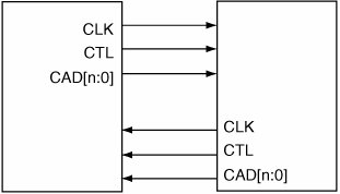
3.1.4. HyperTransportHyperTransport (HT) is a high-speed, point-to-point, chip interconnect technology. Formerly known as Lightning Data Transport (LDT), it was developed in the late 1990s at Advanced Micro Devices (AMD) in collaboration with industry partners. The technology was formally introduced in July 2001. Apple Computer was one of the founding members of the HyperTransport Technology Consortium. The HyperTransport architecture is open and nonproprietary. HyperTransport aims to simplify complex chip-to-chip and board-to-board interconnections in a system by replacing multilevel busses. Each connection in the HyperTransport protocol is between two devices. Instead of using a single bidirectional bus, each connection consists of two unidirectional links. HyperTransport point-to-point interconnects (Figure 32 shows an example) can be extended to support a variety of devices, including tunnels, bridges, and end-point devices. HyperTransport connections are especially well suited for devices on the main logic boardthat is, those devices that require the lowest latency and the highest performance. Chains of HyperTransport links can also be used as I/O channels, connecting I/O devices and bridges to a host system. Figure 32. HyperTransport I/O link Some important HyperTransport features include the following.
HyperTransport was designed to work with the widely used PCI bus standardit is software compatible with PCI, PCI-X, and PCI Express. In fact, it could be viewed as a superset of PCI, since it can offer complete PCI transparency by preserving PCI definitions and register formats. It can conform to PCI ordering and configuration specifications. It can also use Plug-and-Play so that compliant operating systems can recognize and configure HyperTransport-enabled devices. It is designed to support both CPU-to-CPU communications and CPU-to-I/O transfers, while emphasizing low latency. A HyperTransport tunnel device can be used to provide connection to other busses such as PCI-X. A system can use additional HyperTransport busses by using an HT-to-HT bridge. Apple uses HyperTransport in G5-based systems to connect PCI, PCI-X, USB, FireWire, Audio, and Video links. The U3H acts as a North Bridge in this scenario.
3.1.5. Elastic I/O InterconnectThe PowerPC 970 was introduced along with Elastic I/O, a high-bandwidth and high-frequency processor-interconnect (PI) mechanism that requires no bus-level arbitration.[18] Elastic I/O consists of two 32-bit logical busses, each a high-speed source-synchronous bus (SSB) that represents a unidirectional point-to-point connection. As shown in Figure 31, one travels from the processor to the U3H companion chip, and the other travels from the U3H to the processor. In a dual-processor system, each processor gets its own dual-SSB bus. Note that the SSBs also support cache-coherency "snooping" protocols for use in multiprocessor systems.
A synchronous bus is one that includes a clock signal in its control lines. Its communication protocol functions with respect to the clock. A source-synchronous bus uses a timing scheme in which a clock signal is forwarded along with the data, allowing data to be sampled precisely when the clock signal goes high or low. Whereas the logical width of each SSB is 32 bits, the physical width is greater. Each SSB consists of 50 signal lines that are used as follows:
Using 44 physical bits to transmit 36 logical bits of information allows 8 bits to be used for parity. Another supported format for redundant data transmission uses a balanced coding method (BCM) in which there are exactly 22 high signals and 22 low signals if the bus state is valid. The overall processor interconnect is shown in Figure 31 as logically consisting of three inbound segments (ADI, THI, SRI) and three outbound segments (ADO, THO, SRO). The direction of transmission is from a driver side (D), or master, to a receive side (R), or slave. The unit of data transmission is a packet. Each SSB runs at a frequency that is an integer fraction of the processor frequency. The 970FX design allows several such ratios. For example, Apple's dual-processor 2.7GHz system has an SSB frequency of 1.35GHz (a PI bus ratio of 2:1), whereas one of the single-processor 1.8GHz models has an SSB frequency of 600MHz (a PI bus ratio of 3:1). The bidirectional nature of the channel between a 970FX processor and the U3H means there are dedicated data paths for reading and writing. Consequently, throughput will be highest in a workload containing an equal number of reads and writes. Conventional bus architectures that are shared and unidirectional-at-a-time will offer higher peak throughput for workloads that are mostly reads or mostly writes. In other words, Elastic I/O leads to higher bus utilization for balanced workloads.
The Bus Interface Unit (BIU) is capable of self-tuning during startup to ensure optimal signal quality. |
EAN: 2147483647
Pages: 161
