6.4 100BaseTX
| 100BaseTX and 100BaseFX form the subgroup of 100BaseX, which is a part of the 100-Mbps Ethernet group of 100BaseT. Physical layers of both 100BaseTX, which uses two pairs of Category 5 unshielded twisted pair cables, and 100BaseFX, which uses two multimode fibers, are borrowed from existing FDDI standards to save the technology development time. Basics of physical layer 100BaseTX are defined in ANSI X3.263, FDDI Token Ring Twisted Pair Physical Layer, with modifications specified in Ethernet standards 100BaseX and 100BaseTX. The ANSI X3.263 standards define the MLT-3 line code, line voltages, and waveforms, as well as channel and crosstalk models. The 100BaseX standards specify the 4B5B encoding, while the 100BaseTX standards clarify transmit and receive pair connections on the RJ45 connector. With the 4B5B encoding, every 4 bits of information are converted into a 5-bit code resulting in an effective bit rate of 125 Mbps over the transmission media. 100BaseTX uses a higher grade unshielded twisted pair cable of Category 5 instead of the Category 3 cable used by 10BaseT and 100BaseT4. The Category 5 cable is rated for transmission at frequencies up to 100 MHz, while the Category 3 cable is rated for only 16 MHz. In other words, Category 5 cable has less attenuation and crosstalk. On the other hand, signaling at a rate of 125 Mbps requires adaptive channel equalization to compensate for intersymbol interferences caused by amplitude and phase distortions of twisted pair cables of different lengths. The adaptive channel equalization for 100BaseTX transceiver can be implemented in either analog or digital circuits. The digital adaptive channel equalizer performs better but demands a high-speed Analog-to-Digital Convertor (ADC) and digital circuits. 6.4.1 Summary of 100BaseX and 100BaseTX Ethernet StandardsThe 4B5B encoding table is defined in the 100BaseX part of the Ethernet standards and appears here as Table 6.4 for your convenience. There are a few groups of 4B5B codes. The first is the data group of 16 codes that maps any combination of 4 bits to a unique 5-bit code. As far as this group is concerned, the code utilization is 80%. The second is the code group for control purposes that includes character representation of J, K, T, and R. Enough transitions are chosen for the selection of these two code groups to ensure clock recovery in cases when scrambling is not used. The last group is a collection of idle, dead, and error (represented by the character H). Besides other details, the 100BaseX also defines the MAC encapsulation frame. The encapsulation simply adds an SSD (Start-of-Stream Delimitor) and an ESD (End-of-Stream Delimiter) at the beginning and at the end of each MAC frame. The SSD consists of characters of J and K and the ESD consists of characters of T and R.
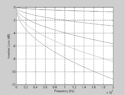
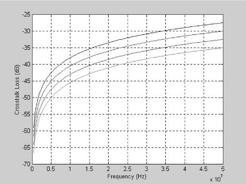
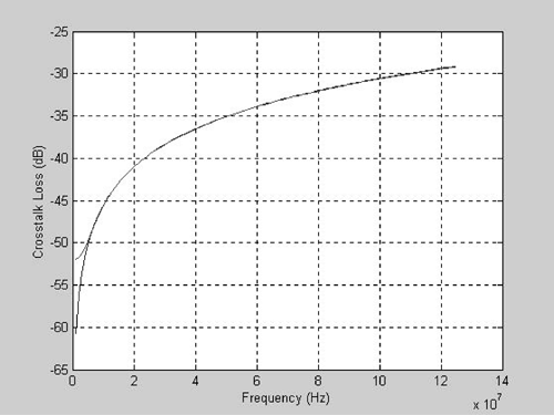
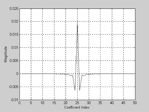
Note that there is no DC balance issue for these 5-bit codes because the MLT-3 encoder will use these codes to drive the line to the +1, 0, or 1 signal level. Each "1" bit in these codes will cause a signal-level transition, and transitions are made in the sequence of ..., 0, +1, 0, 1, 0, +1, . . . . The 100BaseTX standards specify that the transmit and receive pairs should be connected in the same fashion as those defined for 10BaseT. In other words, the transmit pair is connected to pins 1 and 2 and the receive pair is connected to pins 3 and 6 of an RJ45 connector for a conventional NIC card. Similar rules of 10BaseT for crossover cable and hub side connection also apply. 6.4.2 Summary of Relevant FDDI (ANSI X3.263) StandardsInstead of specifying a detailed worst-case Category 5 twisted pair cable channel model, the ANSI X3.263 defines signal attenuations of five Category 5 test cables at the frequency of 16 MHz. These attenuations are 0.5, 2.5, 5, 7.5, and 10 dB and approximately correspond to worst-case loss Category 5 twisted pair cables of lengths 25, 100, 195, 290, and 385 ft, respectively. Figure 6.43 shows insertion losses of these five test cables based on the propagation constant Category 5 twisted pair model. In a similar manner, crosstalk models are also defined as losses of 35, 35, 37.5, 40, and 42.5 dB at 16 MHz corresponding to these test cables of approximate lengths of 25, 100, 195, 290, and 385 ft, respectively. Notice that only four crosstalk models are defined for five different cable lengths. Figure 6.44 shows these four crosstalk models. The 15-dB/decade Category 5 twisted pair cable crosstalk model with a loss of 42.5 dB at 16 MHz can be approximated with a linear phase Finite Impulse Response (FIR) filter. Figure 6.45 shows the insertion loss of this FIR filter as well as that of the 15-dB/decade model. Figure 6.46 shows corresponding filter coefficients in time domain. Figure 6.43. Insertion Losses of Category 5 Test Cables
Figure 6.44. NEXT Losses of Category 5 Test Cables
Figure 6.45. Crosstalk Loss Models
Figure 6.46. Crosstalk Model Impulse Response
A scrambler is used in the transmitter after 4B5B encoding to spread out signal energy, especially during the idle transmit state. A pseudo-random sequence of length 2047 is generated according to Equation 6.20
This pseudo-random sequence can be generated with a shift register of 11 delay elements and initialized with at least one 1. The scrambled stream is created by Exclusive OR operation of the bit out of the 4B5B encoder and a bit of the pseudo-random sequence as follows: Equation 6.21
A descrambling process is required to recover the 4B5B-encoded stream at the receiver. A descrambled stream is obtained by Exclusive OR operation of the received bit and a bit of the same pseudo-random sequence as follows: Equation 6.22
where d(n) is the synchronized pseudo-random sequence and is the received bit. A process at the receiver end is necessary to synchronize the pseudo-random sequence generator to that of the transmitter. A hypothesis stream of 11 bits, h(n), is created by Exclusive OR operation of received bits using Equation 6.23
The pseudo-random sequence generator is loaded with the following pattern: Equation 6.24
when the pattern of h(k:k - 10) = [11111111111] or equivalently c(k:k - 21) = [0101010111101110111111] is detected. After the initial synchronization, the receiver-side pseudo-random sequence generator is independently updated according to the same formula as described by Equation 6.25
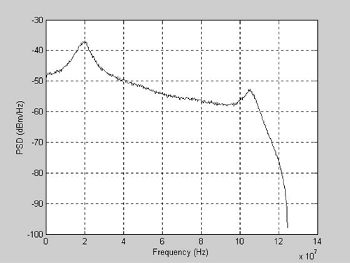
MLT-3 stands for Multi-Level Transition encoding of three levels: negative, zero, and positive. The input to an MLT-3 encoder is a binary sequence consisting of ones and zeros. The corresponding output from the same encoder is a sequence of the same rate but consists of minus ones, zeros, and plus ones. The encoding rules are changing the output signal level for a 1-bit input and keeping the same output signal level for a 0-bit input. An MLT-3 encoder can be implemented with the assistance of a flag in association with these signal levels. The flag is set when the signal level reaches +1 and is reset when it reaches 1. The signal level change direction from zero is decided based on the flag. A 1-bit input causes the output from 0 to 1 if the flag is set and to +1 if the flag is reset. An MLT-3 decoder can be implemented by simply translating a signal-level change to an 1-bit output and generating 0 bits if the signal level stays the same. Line signal shape is defined in terms of a nominal voltage of ±1 V and a nominal rising and falling time of 4 ns in the ANSI X3.263 standards. In comparison, the duration of each bit is 8 ns. Figure 6.47 shows the PSD of the 100BaseTX signal. This PSD shape is pretty unique owing to both 4B5B code word selection and MLT-3 encoding. This PSD has a lower high-frequency spectrum density compared with those of other line codes to meet FCC radio emission requirements at frequencies above 30 MHz. Figure 6.47. 100BaseTX PSD
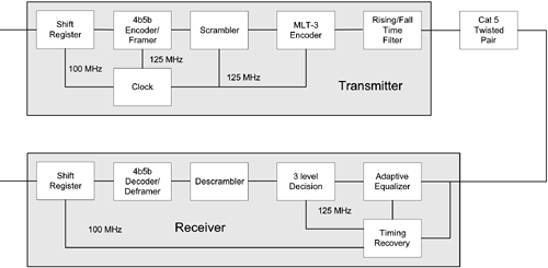
6.4.3 100BaseTX Transceiver Structure and Performance EstimationA possible 100BaseTX transceiver structure is shown in Figure 6.48. The transmit part in the top of the figure consists of a shift register to take information bits in, a 4B5B encoder, a scrambler, an MLT-3 encoder, and a rising/fall time filter. The receive part consists of an adaptive channel equalizer, a timing recovery circuit, a three-level decision device, a descrambler, a 4B5B decoder, and a shift register to send information bits out. Extensive phase and frequency distortions induced by the Category 5 twisted pair cable at a signaling rate of 125 MHz make signal detection impossible without the use of an adaptive channel equalizer. In other words, the eye of the corresponding eye diagram is completely closed at the receiver end. Figure 6.48. 100BaseTX Transceiver Structure
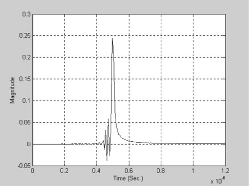
Earlier implementations of 100BaseTX transceivers used an analog adaptive channel equalizer [3]. An adaptive analog equalizer can be realized with three amplifiers of different frequency responses in parallel. The first amplifier's frequency response has a relatively flat slope with a little high gain, 1 dB, at the high-frequency end of the 0- to 30-MHz band. The second amplifier's frequency response has a higher gain, 4 dB, at the high-frequency end. The third amplifier has 8 dB more gain at the high-frequency end. The first amplifier is always active for compensating frequency distortion of short loops. The second amplifier becomes active when longer loops are encountered. When all three amplifiers are active, a total frequency compensation of 13 dB can be provided for longest loops. The activation of these amplifiers are dependent on received signal level and are controlled by a circuit similar to Automatic Gain Control (AGC). An analog phase locked loop is usually associated with an analog adaptive channel equalizer for timing recovery. Digital adaptive channel equalization techniques have been used for most current versions of 100BaseTX transceivers. An ADC is used to sample the received signal at the bit rate of 125 MHz. The length of a digital adaptive equalizer is related to the duration of the longest Category 5 twisted pair cable channel impulse response. Figure 6.49 shows the impulse response of a typical long Category 5 twisted pair cable. The channel delay to the beginning of the impulse response is about 400 ns. We mark the peak of the impulse response as the cursor. The precursor duration (from the beginning to the cursor) of the channel impulse response is then about 100 ns, or 12 samples, and the postcursor duration (from the cursor to the end of the impulse response) is about 400 ns, or 50 samples. The length of a digital channel equalizer is then about 62 taps. Among them, 12 can be feedforward filter taps, and 50, feedback filter taps. Figure 6.49. Category 5 Twisted Pair Cable Channel Impulse Response
Figure 6.50 shows the structure of a decision feedback channel equalizer. The received signal is first sampled by the A/D convertor and sent to the feedforward as its input. Past decisions are sent to the feedback filter as its input. The feedforward filter compensates for reflections in the precursor, while the feedback filter cancels the postcursor based on previous decisions. Feedforward and feedback filter coefficients are adjusted adaptively according to Equation 6.26
Figure 6.50. The Structure of an Adaptive Decision Feedback Channel Equalizer
Equation 6.27
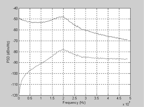
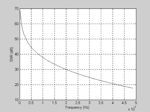
where The timing recovery is a very important part along with the channel equalization. Not just the operation of the equalizer needs to be in synchronization with the baud rate of the received signal, but the sampling phase should also be selected to optimize equalization performance. A traditional analog phase locked loop can be used in conjunction with digital equalization, but some baud rate based digital timing recovery circuits are preferred. Timing information can be recovered from the equalizer output with reference to corresponding signal levels [4]. A digital phase locked loop can then be used to refine the recovered clock signal. The MLT-3 seems like a DC balanced line code except that there is still a slight probability that it can stay at the +1 or 1 level for a long duration. This might occur for a sequence whose scrambled version consists of a long sequence of zeros; therefore, the MLT-3 encoded line voltage will stay at one level during that duration. Since a line transformer is used to couple the transceiver circuit to the twisted pair cable, low-frequency components caused by long zero sequences experience more attenuation. Effectively, a long-lasting +1 or 1 sequence tends to lose its amplitude toward zero. DC wandering compensation circuits are utilized in some transceiver implementations to avoid this problem. The theoretical performance of a 100BaseTX transceiver under the worst-case NEXT environment, as defined by the standards, can be analyzed by comparing the SNR at the front of the receiver. Figure 6.51 shows receiver front-end signal (at the top) and crosstalk PSDs for a frequency band of 0 65 MHz. The propagation constant channel model of 385 ft and the corresponding crosstalk model are used to generate these PSDs, respectively. The corresponding SNR is shown in Figure 6.52. Based on these receiver front-end SNRs, the channel capacity for the 100BaseTX transmission environment is found using Equation 6.28
Figure 6.51. Received Signal and Crosstalk Noise PSD
Figure 6.52. Receiver Front-End SNR
At about 500 Mbps, the channel capacity is about four times the throughput of the 100BaseTX transmission protocol. The performance of a typical 100BaseTX transmission system under different channel and noise environments can be studied through computer simulation. Figure 6.53 shows a 100BaseTX Simulink model block diagram at its highest hierarchical level. This Simulink model consists of a random binary sequence generator as the signal source, a 100BaseTX transmitter to convert the information sequence into MLT-3 encoded line voltage on the twisted pair cable, a Category 5 twisted pair cable channel, and a 100BaseTX receiver. Three scopes are placed right after the information sequence, the transmitter, and the receiver to collect simulation results. Figure 6.53. 100BaseTX Simulink Model
Figure 6.54 shows that the internal structure of the Simulink model transmitter consists of a 4B5B encoder and an MLT-3 encoder. Since the simulation is carried out at a sampling rate of 125 MHz, the rise and fall time filter is omitted. The scrambler and descrambler are also omitted for simplicity. Figure 6.54. Transmitter Model
Figure 6.55 shows the internal structure of the model 4B5B encoder. The serial data stream is converted into 4-bit parallel. Each 4-bit group is used as the input to the 4B5B encoding lookup table. The 5-bit parallel output from the table is reconverted to serial stream. Figure 6.55. 4B5B Encoder
Figure 6.56 shows the internal structure of the model MLT-3 encoder. The 125-MHz clock is masked by the input data. In other words, only input 1's result-to-output signal level changes. Every 125-MHz clock pulse will cause the first D flip-flop on the left to change its output from a 0 to a 1 and vice versa. Using the output of the first D flip-flop as its CLK input, the second D flip-flop changes its output from a 0 to a 1 and vice versa for every two 125-MHz clock pulses. Meanwhile the output of the second D flip-flop determines the sign of the MLT-3 encoder output. A zero output from the second D flip-flop negates the output of the first D flip-flop. Figure 6.56. MLT-3 Encoder
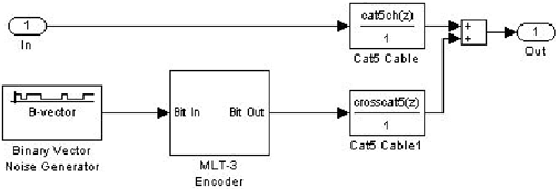
Figure 6.57 shows the Category 5 channel model consisting of a signal attenuation and a crosstalk noise coupling loss. Both are defined by discrete transfer functions which are MATLAB variables preloaded at the activation of this Simulink simulation. The crosstalk model is driven by another MLT-3 encoder emulating a disturbing transmitter. Figure 6.57. Channel Model
Figure 6.58 shows the internal structure of the Simulink model receiver consisting of an adaptive channel equalizer and an MLT-3 decoder. The 4B5B decoder can also be implemented using a lookup table with a structure similar to that of the 4B5B encoder and is omitted because the implementation of bit group synchronization can be quite involved. Also because of the 125-MHz sampling rate simulation, the function of a digital timing recovery circuit is not included in this Simulink simulation model. Figure 6.58. Receiver Model
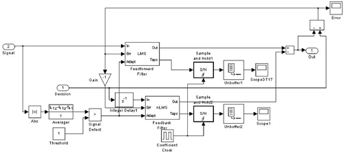
Figure 6.59 shows the internal structure of the adaptive equalizer consisting of a feedforward filter and a feedback filter. A received signal detector is used to activate the adaptation process. There is no training sequence defined in the 100BaseTX standards. The equalizer can be converged during the idle time based on the principle of blind equalization [5] because only three output levels are involved. The convergence can be further assured by preloading some filter coefficients representing some typical Category 5 twisted pair channels. Figure 6.59. Adaptive Equalizer
Figure 6.60 shows the internal structure of the MLT-3 decoder model. The decoder simply generates a 1 bit if two consecutive inputs are not equal and a 0 bit otherwise. Figure 6.60. MLT-3 Decoder
|
EAN: 2147483647
Pages: 97

 is the feedforward filter coefficient vector,
  is the feedback filter coefficient vector,
  is the received signal vector,
  is the previous decision vector, µ1 is the adaptation coefficient for the feedforward filter, and µ2 is the adaptation coefficient for the feedback filter. µ1 and µ2 must be small enough to ensure the convergence of this adaptation LMS (Least Mean Square) algorithm, while their values affect both initial convergence speed and residual error level.