| One of the most important components found on any motherboard is the CPU , or central processing unit . The CPU is the brains of the computer, requesting information from devices, modifying and creating information, and then sending information to devices. It's also the first component your friends will ask you about when you buy a new PC! Recognizing different CPU types is very important in determining -
Which computers are capable of performing certain tasks -
Which computers are obsolete -
Which computers can be updated through a CPU change The following tables provide an overview of CPU types, including their speed, voltage, and socket type. Use Table 4.4 along with the illustrations to help you recognize the major CPUs. tip  | The 2003 version of the A+ Certification Exam covers Pentium, Pentium-equivalent, and newer processors. |
What makes a particular CPU fit (or not fit) into a particular motherboard? The motherboard and processor must both support the same processor type, same voltage, same socket type, and same clock speed. Although adapters can be used to adjust voltage and clock speeds and to convert some slot-based motherboards to use socketed processors of the same processor family, adapters cannot change a CPU's pinout to enable a Pentium 4 to fit in place of an AMD Athlon XP CPU, for example. There are actually two clock speeds that must be considered when you match a processor to a motherboard. Starting with 486DX2 CPUs, CPUs began to have two clock speeds: a core clock speed (the speed at which operations took place inside the CPU) and a slower system bus speed (the speed at which RAM memory was accessed). When comparing systems with similar core clock speeds, the one with the faster system bus speed is preferred because it can access RAM faster. Table 4.4 lists the physical characteristics of major CPU types, starting with the Intel Pentium. Use this table to verify compatibility with motherboards and to make sure that the system is correctly configured. Table 4.4 lists chips in order by socket or slot type used. Most chips on these charts were produced by Intel. Use the footnotes to determine additional manufacturing sources and other notes. The chip types are defined later, in Table 4.5. Table 4.4. Physical Characteristics of Intel Pentium and Newer Processors (Desktop Versions) | Processor | Clock Speed Range | System Bus | Core Voltage | Socket Type | L2 Cache | | Pentium | 6066MHz | Same | 5V | Socket 4 | No | | Pentium | 75200MHz | 50, 60, and 66MHz | 3.3V | Socket 5 , 7 | No | | Pentium MMX | 200233MHz | 66MHz | 2.8V | Socket 7 | No | | AMD K5 | 100166MHz | 66MHz | 3.3V | Socket 5, 7 | No | | AMD K6 | 166300MHz | 66MHz | 2.93.2V | Socket 7, Super 7 | No | | AMD K6-2 | 266550MHz | 66100MHz | 2.2V | Socket 7, Super 7 | No | | AMD K6-III | 400450MHz | 100MHz | 2.4V | Socket 7, Super 7 | Yes | | Cyrix 6x86 | 80150MHz | 4066MHZ | 2.83.52V | Socket 7, Super 7 | No | | Cyrix 6x86MX, MII | 100300MHz | 50100MHz | 2.22.9V | Socket 7, Super 7 | No | | Pentium Pro | 150200MHz | 6066MHz | 3.13.3V | Socket 8 | Yes | | Pentium II | 233333MHz | 66MHz | Auto VRM [1] | Slot 1 | Yes | | Pentium II | 350450MHz | 100MHz | Auto VRM [1] | Slot 1 | Yes | | Celeron | 266400MHz | 66MHz | Auto VRM [1] | Slot 1 | Yes | | Pentium III | 450600MHz | 100MHz | Auto VRM [1] | Slot 1 | Yes | | Pentium III | 600MHz1.1GHz | 100MHz | Auto VRM [1] | Socket 370 | Yes | | Celeron | 300766MHz | 66MHz | Auto VRM [1] | Socket 370 | Yes | | Celeron | 800MHz1.4GHz | 100MHz | Auto VRM [1] | Socket 370 | Yes | | Pentium III | 533MHz1.4GHz | 133MHz | Auto VRM [1] | Socket 370 | Yes | | AMD Athlon | 500MHz1GHz | 200MHz | Auto VRM [1] | Slot A | Yes | | AMD Athlon | 650MHz1GHz | 200MHz | Auto VRM [1] | Socket A | Yes | | AMD Athlon | 11.4GHz | 266MHz | Auto VRM [1] | Socket A | Yes | | AMD Duron | 550MHz1.3GHz | 200MHz | Auto VRM [1] | Socket A | Yes | | AMD Athlon XP | 1.333GHz (1500+)2.2GHz (3200+) [2] | 266MHz, 333MHz, 400MHz | Auto VRM [1] | Socket A | Yes | | Pentium 4 | 1.31.8GHz [2] | 400MHz | Auto VRM [1] | Socket 423 | Yes | | Pentium 4 | 1.43.2GHz [2] | 400MHz, 533MHz, 800MHz | Auto VRM [1] | Socket 478 | Yes | | Celeron | 1.72.4GHz [2] | 400MHz | Auto VRM [1] | Socket 478 | Yes | [1] Voltage level set by processor [2] Processor in current production; maximum speeds listed might increase As you prepare for the A+ Certification Exam, note in particular the processor sockets and speed ranges used by each processor. Note also that the Celeron name actually refers to a series of low-cost (slower, less L2 cache) versions of the Intel Pentium II, Pentium III, and Pentium 4 processors. tip  | So-called "Super 7" or "Super Socket 7" motherboards use the standard Socket 7 processor socket, but also add support for different voltages and processor/system bus speeds required by Pentium-class processors from AMD and Cyrix. |
Core Voltage The core voltage is the voltage that the motherboard feeds to the processor. Most Socket 5, Socket 7, and Super Socket 7compatible CPUs use a variety of different voltage settings, depending on clock speed and design revisions. Motherboards that use these CPUs must be used with voltage regulators set to the correct voltage to avoid CPU damage. Voltage regulators are built into many motherboards, or they can be "sandwiched" between the CPU socket and the CPU. Voltage regulators must be set to the correct voltage for the particular CPU model installed or the CPU can be damaged. caution  | Some processors are marked with two voltage levels: the core and the I/O. Make sure you set the voltage regulator to the core (lower) voltage level. Set a processor that is supposed to run at 2.2V to run at 3.3V, and you'll have a fried processor! |
Fortunately, CPUs that use Socket 370, Slot 1, Slot A, or Socket A feature automatic voltage regulation, enabling the CPU to set the correct operating voltage without any "help" from the user. Some motherboards using these CPUs might enable the user to vary the voltage from the default settings for special purposes. Note that early motherboards might not be able to adjust to the voltage requirements of some later processors in a particular processor family. caution  | Most processors listed in Table 4.4 represent different families of models that use different voltage levels and processor sockets/slots. You should physically examine any system and check its documentation to verify the exact CPU type and socket in use and to determine compatible processors before replacing or upgrading the CPU. |
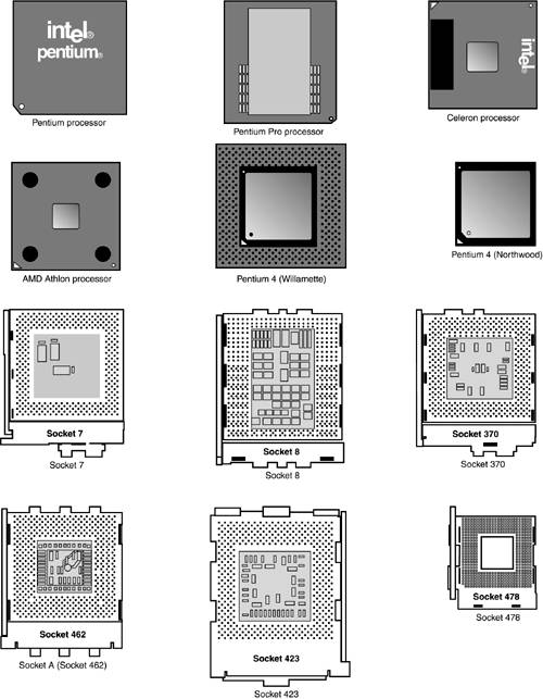
Physical CPU Packaging Types CPUs have been packaged in many different forms since the first IBM PC was produced in 1981. During the lifespan of any given CPU, more than one physical packaging type can be used. Thus, you always should physically examine a system that you want to upgrade with a new CPU. Make sure you determine which slot or socket type it has so you know which packaging type to ask for. Some desktop computers have soldered CPUs that cannot be removed for replacement or upgrading. Table 4.5 defines the packaging types used for both older and current processors, as seen previously in Table 4.4. Table 4.5. Major Physical Chip Packaging Types | Package Type | Major Uses | Package Name and Note | | DIP | 8088, 8086 | Dual Inline Pin. | | Early 80287 math co-processors | A rectangular, ceramic chip with easily bent thin metal legs down the long sides of the chip. A recessed "dimple" at one end corresponds with a similar cutout at one end of the socket for keying. | | This packaging type is no longer used for CPUs but is still used for BIOS (firmware) chips used on motherboards, video cards, SCSI host adapters, and network cards. BIOS DIPs have fewer pins than CPU DIPs, and often have a sticker indicating the manufacturer over the top of the chip. | | PLCC | 80286, 80387SX math co-processor | Plastic Leaded Chip Carrier. | | BIOS chip (recent systems) | A square, ceramic chip with protruding contacts on all four sides. These slightly springy metal contacts hold the chip in place but don't provide a reliable keying method; a special PLCC chip puller is recommended if you work on systems using these types of chips. | | PQFP | 80386SX | Plastic Quad Flat Pack. | | BIOS chip (recent systems) | A square, ceramic chip that resembles the PLCC but is surface-mounted to the motherboard. | | PGA | 80486DX, 80386DX | Pin Grid Array. | | Pentium 60 and 66, Pentium Pro, most later models | A square, ceramic chip with several rows of pins on the underside, leaving the middle open . Introduced with some 80286 models, PGA is also the basis for all subsequent socketed processors from the Pentium 75MHz all the way through the latest Pentium 4 and AMD Athlon XP processors. See "PGA Variations," later in this chapter. | | SECC | Early Pentium II | Single Edge Contact Cartridge. | | The first slot-mounted CPU in the Intel family, the cartridge is a shell that encloses an SEC (Single Edge Contact) module with the Pentium II CPU and Level 2 cache. | | Other slot-mounted packages used for later Pentium II, Pentium III, and Celeron include SECC2 (simplified design) and SEPP (no cartridge shell). Adapters using SEPP are available to enable PPGA-based Celeron and Pentium III processors to attach to Slot 1 motherboards. | PGA Variations The PGA chip/socket design is the basis for all recent socketed chips. Some socketed chips move the processor core to the top of the processor for better cooling. These include FC-PGA (Flip-Chip Pin Grid Array) and FC-PGA2 used by some Socket 370 (Pentium III and Celeron) processors; AMD Athlon and Duron (Socket A) and all Socket 478 processors (Pentium 4 and Celeron); OLGA (Organic Land GA) used by Socket 423 Pentium 4 processors; and OPGA (Organic Pin Grid Array) used by AMD Athlon XP. Socket and Slot Types Most Pentium-class and newer CPUs fit into square sockets of various types (the Pentium Pro's socket is rectangular); see Figure 4.12 for a comparison of these sockets. These sockets have different pinouts and electrical characteristics, making it important that you match the CPU you want to use to the sockets designed to handle it. You should note the most popular CPUs that use each socket type for the test (see Table 4.6). Figure 4.12. Processors and sockets from Pentium to Pentium 4.  Table 4.6. CPU Socket Types for Pentium and Newer CPUs | Socket Type | For CPU Types | Number of Pins | Voltage | | Socket 4 | Pentium 60/66 | 273 | 5V | | Socket 5 | Pentium 75133, OverDrive | 320 | 3.3/3.5V | | Socket 7 [1] | Pentium 75233, MMX; AMD K5, K6; Cyrix 6x86, MII | 321 | Uses voltage regulator on motherboard | | Socket 8 | Pentium Pro | 387 | Automatic voltage regulation | | Socket 370 (PGA 370) | Celeron; Pentium III [2] VIA C3 | 370 | Automatic voltage regulation | | Socket A (Socket 462) | Athlon, Duron, Athlon XP | 462 | Automatic voltage regulation | | Socket 423 | Pentium 4 (early version) | 423 | Automatic voltage regulation | | Socket 478 | Pentium 4 (current), Celeron | 478 | Automatic voltage regulation | | Socket 603 | Xeon | 603 | Automatic voltage regulation | [1] Super Socket 7 is an unofficial term for Socket 7 motherboards, which support processors faster than 233MHz (AMD K6 and Cyrix 6x86, 6x86MX, and MII) . [2] There are three versions of Socket 370 that vary by pin assignment and voltage. Verify processor compatibility for a particular Socket 370 motherboard before you upgrade processors. Starting with Socket 3 (used for 486 CPUs), CPU sockets typically feature a so-called Zero Insertion Force (ZIF) socket design, with a handle that you raise to release the CPU and lower to clamp the CPU in place. tip  | Most CPU sockets have the socket name molded into the top of the socket for easy identification. |
Table 4.7 lists the major CPU slot types. Slot-mounted processors are no longer produced, although many systems using slot-mounted processors are still in use. Table 4.7. CPU Slot Types | Slot Type | Also Known As | For CPU Types | | Slot 1 [1] | SEC-242 | Intel Pentium II, Celeron | | Slot A | N/A | AMD Athlon | | Slot 2 | SEC-330 | Intel Pentium II Xeon, Pentium III Xeon | [1] Adapters known as slot-kets can be used to adapt Socket 370 processors for use on Slot 1 motherboards. Internal CPU Characteristics Affecting Performance Besides core and bus clock speeds, there are other factors that influence the true speed of a CPU: -
The register size and data bus These refer to the width of data that can be accessed in each CPU operation; the register size refers to data management inside the CPU, whereas the data bus refers to data transfer between the CPU and RAM. Some CPUs have a bottleneck created by having a data bus narrower than the register size; having a data bus wider than the register size increases speed by enabling the CPU to perform two data-transfer operations at the same time. -
The presence or absence of a math co-processor circuit to perform faster floating-point math (used by CAD and spreadsheet programs ) Although most CPUs prior to the Pentium used a separate math co-processor, the Pentium and all newer CPUs covered on the A+ Certification Exam have a built-in math co-processor. -
The amount of RAM the CPU can access Larger amounts are better, although the actual motherboard design limits most systems to far less RAM than the CPU can use. -
The presence or absence of cache RAM (RAM that holds a copy of main memory for faster access by the CPU ) L1 cache is part of the CPU itself; Level 2 cache is found in various locations as listed in Table 4.8. Small L2 cache sizes or no L2 cache at all slows down the system. -
The amount and speed of cache RAM Larger and faster cache RAM improves system speed, especially for operations that take place entirely or primarily in RAM. Table 4.8. Locations for Level 2 Cache | Processor Model | Level 2 (L2) Cache Location | Notes | | Pentium, Pentium MMX, AMD K5, AMD K6, K6-2 | Motherboard | Size and type varies; some motherboards have removable cache chips or no cache, whereas others have permanently installed cache. | | K6-III | Processor | This model is rare. | | Pentium Pro | Processor | L2 cache runs at full processor speed. | | Pentium II, Celeron 300A and faster, Pentium III (Slot 1 versions) | Processor assembly | L2 cache runs at half processor speed. | | Celeron 266300 (non-A) | None | Lack of L2 cache causes very slow performance. | | AMD Athlon (Slot A) | Processor assembly | L2 cache runs at half or less of processor speed. | | Pentium III, Celeron (Socket 370); AMD Athlon (Socket A), Duron, Athlon XP (all); Pentium 4, Celeron (all) | Processor die | On-die L2 cache runs at full processor speed. | Table 4.9 reviews these internal characteristics of the same CPUs listed in Table 4.8. Check out Table 4.9 when you need to determine the best optimization methods for a given CPU and when looking for CPUs for servers and other tasks requiring large amounts of memory. Note that CPUs used in notebook computers might have different specifications. For the A+ Certification Exam, you should know which processors include both L1 and L2 cache.  | For more information on how cache memory works, see "Cache RAM and Main Memory," p. 240 . |
All processors listed in Table 4.9 have built-in math co-processors, 32-bit internal registers (they handle 32 bits of data internally), and a 64-bit external data bus. However, they vary in the maximum amounts of memory supported, the size of L1 cache, and the presence (and speed) of L2 cache. Table 4.9. Internal Characteristics of Major CPUsPentium and Newer | CPU | Max Memory | L1 and L2 Cache | L2 Cache Speed | | Pentium | 4GB | 16KB - L1 | N/A | | Pentium MMX | 4GB | 32KB - L1 | N/A | | AMD K5 | 4GB | 16KB - L1 | N/A | | AMD K6 | 4GB | 64KB - L1 | N/A | | AMD K6-2 | 4GB | 64KB - L1 | N/A | | Pentium Pro | 64GB | 16KB - L1; 256KB, 512KB, 1GB - L2 | CPU speed | | Pentium II | 64GB | 32KB - L1 512KB - L2 | Half CPU speed | | Pentium III | 64GB | 32KB - L1 512KB - L2 | Half CPU speed | | Pentium III | 64GB | 32KB - L1 256KB - L2 | Full CPU speed | | "Coppermine" Pentium III | 64GB | 32KB - L1 512KB - L2 | Full CPU speed | | "Tualatin" Celeron (266300MHz) | 64GB | 32KB - L1 | N/A | | Celeron [1] (300A and up) | 64GB | 32KB - L1 128KB - L2 | Full CPU speed | | Celeron [2] | 64GB | 32KB - L1 256KB - L2 | Full CPU speed | | AMD Athlon Slot A | 8TB | 128KB - L1 512KB - L2 | Half to one third CPU speed | | AMD Athlon Socket A | 8TB | 128KB - L1 512KB - L2 | Full CPU speed | | AMD Duron | 8TB | 128KB - L1 64KB - L2 | Full CPU speed | | AMD Athlon XP | 8TB | 128KB - L1 256KB - L2 | Full CPU speed | | AMD Athlon XP "Barton" | 8TB | 128KB - L1 512KB - L2 | Full CPU speed | | Intel Pentium 4 | 64GB | 20KB - L1 256KB - L2 | Full CPU speed | | Intel Celeron [3] | 64GB | 20KB - L1 128KB - L2 | Full CPU speed | | Intel Pentium 4 HT Tech [4] | 64GB | 20KB - L1 512KB - L2 | Full CPU speed | [1] Slot 1 and Socket 370 versions are based on the Pentium II/III . [2] Socket 370 version is based on the Pentium III "Tualatin" (has large heat spreader across most of the processor top) . [3] Socket 478 version of the Celeron is based on the Pentium 4. [4] HT Technology versions of the Pentium 4 can simulate a dual-processor computer with just one processor. As you can see from Table 4.9, different versions of a processor might have significant differences in the size and speed of L2 cache. The size and speed of L2 cache should be considered when selecting a new processor for a system. Note also that the Celeron and AMD Duron processors are economy versions of the Pentium II/III/4 and AMD Athlon/Athlon XP. Moving from a Socket 478 Celeron to a Pentium 4 and from a Duron to an Athlon XP processor boosts L2 cache size and usually increases processor speed as well. CPU Installation and Removal CPUs are one of the most expensive components found in any computer. Because a CPU can fail, or more likely, need to be replaced with a faster model, knowing how to install and remove CPUs is important. On the A+ Certification Exam, you should be prepared to answer questions related to the safe removal and replacement of Pentium-class or higher CPUs. The methods used for CPU removal vary according to two factors: the CPU type and the socket/slot type. As you saw in Tables 4.4 and 4.5, almost all CPUs are socketed. Before the development of the ZIF socket , the processor was held in place by tension on the chip's legs, pins, or leads. Thus, to remove these chips, you must pull the chip out of the socket. Because the chip's legs, pins, or leads are fragile, special tools are strongly recommended for removing chips that are not mounted in ZIF sockets. Refer to Table 4.4 for a definition of each of the following physical chip packaging types; Table 4.5 cross references chip types to the recent CPU types that use them. Before removing and installing any CPU or other internal component, be sure to review and follow the ESD precautions discussed in Chapter 13, "Safety and Recycling." PGA-Type CPUs (Pentium, Pentium Pro, and Later Models)No ZIF Socket Pentium-class and newer socketed processors (refer to Table 4.4) use some version of the PGA (Pin Grid Array ) design (refer to Table 4.5) and are usually installed in ZIF sockets; these sockets have a handle that can be lifted to release the processor. However, you might encounter a few Pentium-class processors that are not installed in ZIF sockets. You should use a chip extractor to remove these processors from their sockets. If the CPU has a removable heatsink or fan that is attached to the motherboard, remove the heatsink before removing the CPU. These heatsinks have a horizontal bar that attaches to the motherboard on two sides of the CPU. Squeeze or push the clip down at one end to release the bar and work it loose from the other side of the CPU. Then, disconnect the CPU fan (if included) from its power source and lift the assembly away. Then use one or two PGA chip extractors to remove the PGA chip; this tool resembles a small rake. These extractors are often supplied with 486 or Pentium-class chip upgrades. -
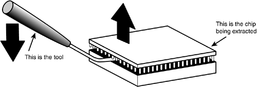
Slide the chip extractor's "fingers" under any side of the CPU (see Figure 4.13). If you have two chip extractors, place the second one on the opposite side of the CPU. Figure 4.13. Insert the PGA chip extractor under the side of the CPU and gently push down on the handle to loosen the CPU; move the extractor to the opposite side and repeat until the chip can be removed.  -
Push gently down on the handle of the chip extractor to pry up the CPU. If you have only one extractor, move the extractor to the opposite side and repeat; do not try to remove the chip with a single application of the extractor because the uneven force will bend the CPU's pins and might damage the socket. -
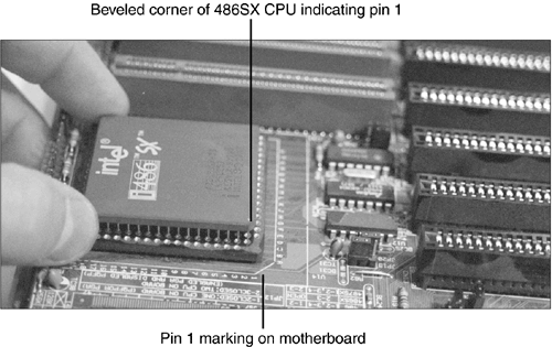
Repeat until the chip is free; place it in antistatic packaging. With the old chip removed, it's time to install a new chip. To insert a PGA-type CPU into a motherboard without a ZIF socket, find the corner of the chip that is cut off (beveled) and might also be marked with a dot; this indicates pin 1. The underside of some chips might be marked with a line pointing toward pin 1. Then follow these steps: -
Line up the pin 1 corner with the corner of the socket also indicated as pin 1 (look for an arrow or other marking on the motherboard). If you put the chip in with pin 1 aligned with the wrong corner and apply the power, you will destroy the chip. -
Gently press the chip into the socket. Make sure you are pressing evenly on all sides of the chip because uneven force will cause pins to bend. Stop when the chip is firmly in the socket (see Figure 4.14). Figure 4.14. Line up the beveled corner (also marked with a dot) of a socketed CPU with pin 1 on the socket.  -
Attach the heatsink or fan if required at this time. PGA-Type CPU in a ZIF Socket ZIF sockets are used on almost all desktop systems using Pentium-class or newer socketed processors including the Athlon XP and Pentium 4. They allow easy installation and removal of the CPU. What makes ZIF sockets easy to work with? They have a lever which, when released, loosens a clamp that holds the CPU in place. If the CPU has a removable heatsink or fan that is attached to the motherboard, remove the heatsink before removing the CPU. Some of these heatsinks have a horizontal bar that attaches to the motherboard on two sides of the CPU. Others, such as the one shown in Figure 4.13, have a spring-loaded clip on one side and a fixed lug on the opposite side. Pentium 4 and Celeron processors that use Socket 478 use heatsinks that attach to a frame around the processor. Here's how to remove the heatsink and the processor: -
Push the clip or bar down at one end to release it and work it loose from the other side of the CPU. With Socket 478, release the screws that hold the CPU fan to the motherboard. -
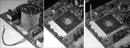
Disconnect the active heatsink (if included) from its power source and lift the assembly away (Figure 4.15). Figure 4.15. After the heatsink fan is disconnected from power (left) to reveal the processor (center), the lever on the ZIF socket (right) can be lifted to release the processor.  -
Push the lever on the ZIF socket slightly to the outside of the socket to release it. -
Lift the end of the lever until it is vertical (see Figure 4.15). This releases the clamping mechanism on the CPU. -
Grasp the CPU on opposite sides, making sure not to touch the pins, and remove it from the socket. Put it into antistatic packaging. To insert a PGA-type CPU into a ZIF socket, find the corner of the chip that is marked as pin 1 (usually with a dot or triangle). The underside of some chips might be marked with a line pointing toward pin 1. Then follow these steps: -
Line up the pin 1 corner with the corner of the socket also indicated as pin 1 (look for an arrow or other marking on the motherboard). If you put the chip in with pin 1 aligned with the wrong corner and apply the power, you will destroy the chip. -
Make sure the lever on the ZIF socket is vertical; insert the CPU into the socket and verify that the pins are fitting into the correct socket holes. -
Lower the lever to the horizontal position and snap it into place to secure the CPU. -
Before attaching the heatsink or fan, determine if the heatsink has a thermal pad (also called a phase-change pad) or if you need to apply thermal compound to the processor core (refer to Figure 4.15). Remove the protective tape from the thermal pad or apply thermal compound as needed. Attach the heatsink or fan. -
To secure the heatsink or fan on motherboards other than those using Socket 478, make sure that the retaining clip is securely in place around the lug on one side of the processor socket. Then, push down the locking clip until it fastens to the locking lug on the other side. For Socket 478, remove the old heatsink mounting mechanism if necessary, install the new one, and attach the heatsink to the mounts on the support mechanism. Slot-Type CPU (SECC, SECC2, SEPP, or AMD Athlon Slot A) You won't see many slot-type CPUs anymore, but if you need to install one on a motherboard, make sure the motherboard has a retention mechanism attached. If the motherboard doesn't have one, you will need to remove the motherboard from the case to attach a retention mechanism. To remove a slot-type CPU -
Push down on the retainers at each end of the CPU to release the CPU from the retention mechanism. -
Disconnect the power lead to the CPU fan (if present). -
Remove the CPU and fan/heatsink from the retention mechanism. The CPU slides straight up from the slot. To attach a slot-type CPU -
Attach the CPU retention mechanism to the motherboard. Leave the foam backing on the bottom of the motherboard while pushing the supports into place. Lift up the motherboard and secure the retention mechanism with the screws supplied. Some motherboards are shipped with the retention mechanism already installed, so this step might not apply to you. If the retention mechanism is folded against the motherboard, unfold it so the supports stand straight up. -
Attach the fan and heatsink to the CPU if not already attached; some CPUs have a factory-attached heatsink/fan, whereas others require you to add it in the field. -
Match the pinouts on the bottom of the CPU to the motherboard's slot; note that the slot has two sides of unequal length, making it easy to match the slot with the CPU. -
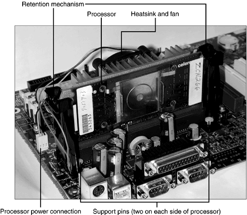
Insert the CPU into the retention mechanism; push down until the retaining clips lock the CPU into place. Figure 4.16 shows the CPU in place. Figure 4.16. A Slot 1based Celeron CPU after installation. The heatsink and fan are attached to the rear of the CPU.  -
Connect the power lead from the fan (if present) to the motherboard or drive power connector as directed. |
