Processor Socket and Slot Types
| If you are building your own server or upgrading it with additional processors, it's very important that you understand the processor packaging and socket, or slot type, used by your server. If you do not know what processor socket (or slot) your server uses, you might purchase an incompatible processor for your server. If you do not know how the processor is packaged, you might purchase an incompatible heatsink or other cooling solution. Today, it's more important than ever before to know these details. With server processors such as the Intel Pentium 4, AMD Opteron, and others being produced in two or more form factors at various points of their development, the odds of buying the wrong processor or cooling solution are higher than they once were. The following sections put particular emphasis on Intel and AMD server processor packaging and motherboard connectors because these are the most common processors used in build-it-yourself or upgrade-it-yourself servers. Many processors are available in a variety of clock speeds and cache sizes, enabling you to boost performance by swapping a faster or larger-cache-size processor for one that is slower or has a smaller cache size. Note Processors in RISC-type servers are generally built in to processor cartridges that contain cache memory. They are not purchased from component vendors as x86 and Itanium processors can be but are sold by the server vendor. For information about compatible processors and processor upgrades for a RISC-based server, contact your server vendor. Overview of x86 and Itanium Server Processor and Socket TypesIntel and AMD have created a set of socket and slot designs for their processors. Each socket or slot is designed to support a different range of original and upgrade processors. Table 2.14 shows the specifications of sockets used for x86 and Itanium server processors, starting with the Intel Pentium Pro.
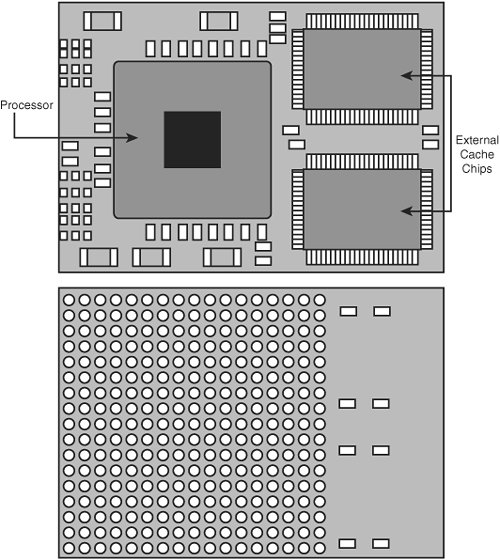
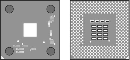
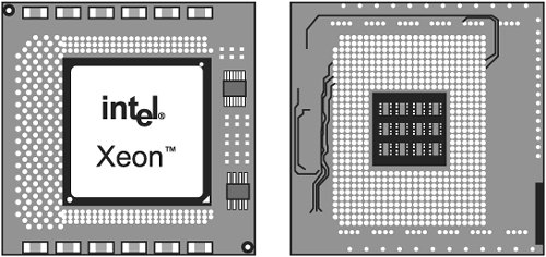
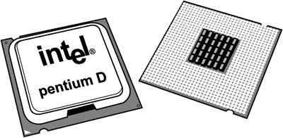
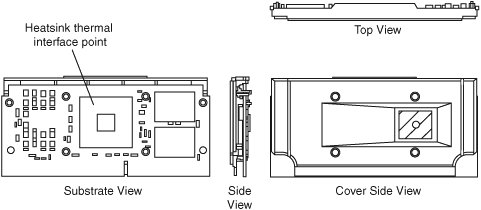
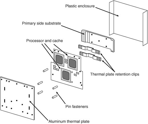
PackagingThe most common packaging type used for x86 and RISC-based processors over the past decade has been the pin grid array (PGA) design. PGA can be subdivided into several categories, reflecting advances in processor design and the never-ending quest for better cooling. Other types of processor packaging include ball grid array (BGA) and land grid array (LGA), which are used as alternatives to PGA in some of the most recent processor designs. Older x86 as well as Itanium and RISC processors also used various types of processor cartridges, which incorporate the processor itself and external cache memory. While x86 processors no longer use processor cartridges, some types of RISC and Itanium-based systems still use subassemblies that incorporate large amounts of cache and the processor. In some cases, a processor cartridge might incorporate two separate processors. The following sections provide details about the major types of processor packaging used on servers. PGA and PGA VariationsPGA, which dates back to the IBM 286 processor first introduced in 1984, takes its name from the fact that the chip has a grid-like array of pins on the bottom of the package. PGA chips are inserted into sockets, which are often of a zero insertion force (ZIF) design. A ZIF socket has a lever to allow for easy installation and removal of the chip. As Figure 2.9 illustrates, PGA designs can be used for modules that contain the processor and external cache as well as for individual processors (compare Figure 2.9 to Figures 2.10 and 2.11). Figure 2.9 illustrates the front and rear view of a PGA-based processor module, the PowerPC 750. Figure 2.9. Top and bottom views of the PowerPC 750 processor module, which includes the processor and two external cache chips. The processor module connects to the system via a PGA socket. Figure 2.10. Top (left) and bottom (right) views of the Athlon MP processor. This processor uses an SPGA connector. Figure 2.11. Top (left) and bottom (right) views of the Xeon DP processor. This processor uses FC-PGA2 packaging. Depending on the processor, the pins might be in standard rows and columns, as in Figure 2.9 and Figure 2.11, or might be staggered. This type of design is known as staggered PGA (SPGA). This design moves the pins closer together and decreases the overall size of the chip when a large number of pins is required. Figure 2.10 illustrates the SPGA design used by the AMD Athlon MP processor. Several methods have been used to build PGA chips. Older PGA variations had the processor die mounted in a cavity underneath the substrate, with the top surface facing up if you turned the chip upside-down. The die was then wire-bonded to the chip package, with hundreds of tiny gold wires connecting the connections at the edge of the chip with the internal connections in the package. After the wire bonding, the cavity was sealed with a metal cover. This was an expensive and time-consuming method of producing chips, so less expensive and more efficient packaging methods were designed. More modern processors are built on a form of flip-chip PGA (FC-PGA) packaging. This type still plugs in to a PGA socket, but the package itself is dramatically simplified. With FC-PGA, the raw silicon die is mounted facedown on the top of the chip substrate, and instead of wire bonding, the connections are made with tiny solder bumps around the perimeter of the die. The edge is then sealed with a fillet of epoxy. With the original versions of FC-PGA, you could see the backside of the raw die sitting on the chip. The Athlon MP chip shown in Figure 2.10 uses an FC-PGA design. Unfortunately, there were some problems with attaching the heatsink to an FC-PGA chip such as an Intel Pentium III or AMD Athlon MP. The heatsink sat on the top of the die, which acted as a pedestal. If you pressed down on one side of the heatsink excessively during the installation process (such as when you were attaching the clip), you risked cracking the silicon die and destroying the chip. This was especially a problem as heatsinks became larger and heavier and the force applied by the clip became greater. AMD decreased the risk of damage to the AMD Athlon MP and similar chips by adding rubber spacers to each corner of the chip substrate (as shown in Figure 2.10), thus preventing the heatsink from tilting excessively during installation. Still, these bumpers could compress, and it was too easy to crack the die during heatsink installation. Intel revised its packaging with a newer FC-PGA2 version used in the newer Pentium III and all Pentium 4 and Xeon processors. It incorporates an integrated protective metal cap called a heat spreader that sits on top of the die, enabling larger and heavier heatsinks to be installed without any potential damage to the processor core. Ironically, the first processor for PCs to use a heat spreader was made by AMD (the K6 family). AMD has returned to the heat spreader design with its Opteron processors. Figure 2.11 illustrates the FC-PGA2 packaging used by the Intel Xeon DP processor. AMD Opteron, Intel Xeon, and Intel Pentium 4 processors also use various types of heatsink supports rather than fastening the heatsink directly to the processor socket. This helps prevent damage to the processor. In addition to changes in the socket and arrangement of the processor core, PGA-based designs have also used various materials for the processor chip substrate. Ceramic material was common for several years, but more recent designs have used lighter-weight plastics, including some organic plastics. Starting in the late 1990s, some processors began to use a different type of connection known as a BGA. BGA chips use small solder balls to make the connection to the socket. BGA is also used to attach DDR and newer types of memory chips to DIMM modules or graphics cards. Typically, BGA is used when chips are soldered into place, such as on a processor module, as shown in Figure 2.9. A variation on BGA known as LGA is used by processors that use Socket 775, such as the latest version of the Intel Pentium 4, as well as the new Pentium D and Pentium Extreme Edition. LGA uses gold pads (called lands) on the bottom of the substrate to replace the pins used in PGA packages or the solder balls used in BGA. In socketed form, LGA allows for much greater clamping forces and therefore greater stability and improved thermal transfer (better cooling) than PGA. Figure 2.12 illustrates the front and rear of the Pentium D, which uses an LGA design. Figure 2.12. Top (left) and bottom (right) views of the Pentium D processor. This processor uses an LGA design. Note Although RISC-based processors typically use PGA or BGA designs, the socket is usually on a small board that also contains cache memory chips. The processor assembly is then plugged in to a slot in the server. Single-Edge Contact Cartridge PackagingIntel used cartridge- or board-based packaging for several of its server-class processors from 1997 through 2000. This packaging was called single-edge contact cartridge (SECC), and it consisted of the CPU and separate L2 cache chips mounted on a circuit board that looked similar to an oversized memory module and that plugged in to a slot. In some cases, the boards were covered with plastic cartridge covers. Building the processor into a cartridge was a cost-effective method for integrating L2 cache into the processor before it was feasible to include the cache directly inside the processor die. Intel used two types of slots for its server-class processors:
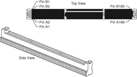
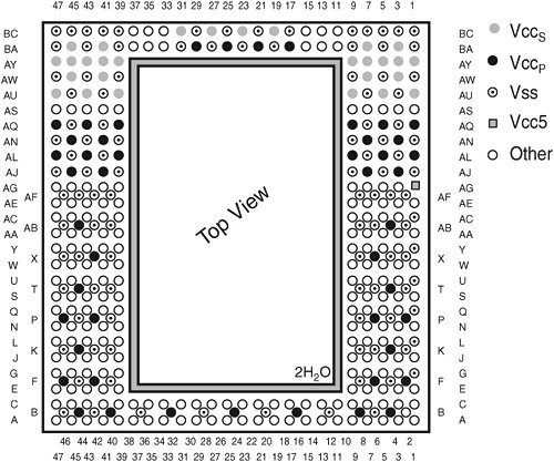
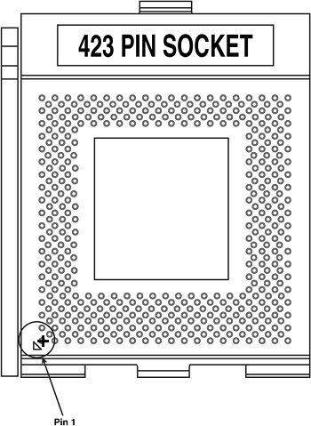
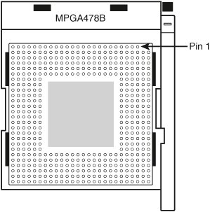
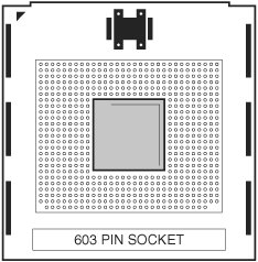
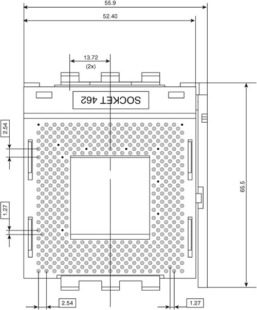
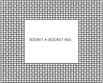
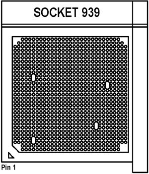
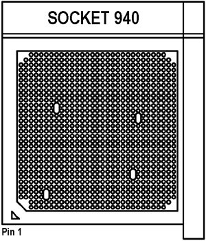
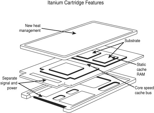
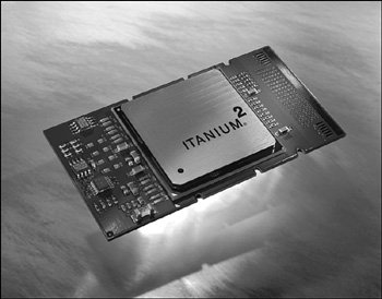
Slot 1 was also known as Slot 242, for the 242 pins in the slot connector. The connector used two different-sized sections to prevent incorrect insertion of the cartridge (see Figure 2.13). A rigid or folding frame known as a processor-retention mechanism was used to support the processor. Slot 1 supported single or two-way processor configurations. Figure 2.13. Slot 1 connector dimensions and pin layout.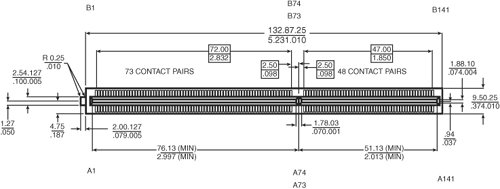 Slot 2 was a more sophisticated 330-pin slot designed for the Pentium II Xeon and Pentium III Xeon processors manufactured for servers and workstations. Slot 2 supported up to four-way processing. Note that Slot 2 was also called SC330, which stands for slot connector with 330 pins (see Figure 2.14). Figure 2.14. Slot 2 (SC330) connector dimensions and pin layout. Intel later discovered less-expensive ways to integrate L2 cache into the processor core, and it no longer produces Slot 1 or Slot 2 processors. Both Slot 1 and Slot 2 processors are now obsolete, and most systems using these processors have been retired or upgraded with socket-based motherboards. Slot 1 (SECC and SECC2) PackagingOriginally, the SECC package wrapped around three sides of the processor cartridge assembly. However, this design made cooling difficult and raised the cost of the processor. Later versions of the Pentium II and all slot-based versions of the Pentium III used a simplified one-piece design known as SECC2. Figure 2.15 illustrates the SECC2 design. The rectangular chips on the right side of the rear view are the cache memory chips. Note the large thermal plate used to aid in dissipating the heat from this processor. A passive or active heatsink was attached to the thermal plate. The SECC2 design used a different type of retention mechanism (the universal retention system) than the original SECC design that also worked with SECC processors. Figure 2.15. SECC2 packaging used in newer Pentium II and III processors. Slot 2 PackagingThe Pentium II Xeon and Pentium III Xeon processors are designed in a cartridge similar to but larger than that used for the standard Pentium II/III. Figure 2.16 shows the Xeon cartridge. Figure 2.16. Pentium II/III Xeon cartridge. Slot 2 versions of the Pentium II Xeon and Pentium III Xeon differ from the standard Pentium II and slot-based Pentium III mainly by virtue of having full-corespeed L2 cache, and in some versions, a larger amount of it. The additional pins allow for additional signals needed by multiple processors. ZIF SocketsWhen the Socket 1 specification used by the first 486 processors was created, manufacturers realized that if users were going to upgrade processors, they had to make the process easier. The socket manufacturers found that 100 pounds of insertion force is required to install a chip in a standard 169-pin screw Socket 1 motherboard. With this much force involved, you could easily damage either the chip or the socket during removal or reinstallation. Therefore, some motherboard manufacturers began using low insertion force (LIF) sockets, which required only 60 pounds of insertion force for a 169-pin chip. But pressing down on the motherboard with 60 to 100 pounds of force can still crack the board if it is not supported properly. A special tool is also required to remove a chip from one of these sockets. As you can imagine, even the LIF was relatively difficult to work with, and a better solution was needed if the average person was ever going to replace his or her CPU. Manufacturers began using ZIF sockets in Socket 1 designs, and all processor sockets from Socket 2 and higher have been of the ZIF design. ZIF is required for all the higher-density sockets because the insertion force would simply be too great otherwise. ZIF sockets almost eliminate the risk involved in installing or removing a processor because no insertion force is necessary to install the chip, and no tool is needed to extract one. Most ZIF sockets are handle actuated: You lift the handle, drop the chip into the socket, and then close the handle. This design makes installing or removing a processor an easy task. Note Although removing a processor from a ZIF socket is simple, it is necessary to remove the heatsink from the processor before the processor itself can be removed. If the heatsink has a fan, it must be disconnected from the motherboard or other power source as well. Heatsinks for some processor types clip directly to the processor socket, and if the spring-loaded arm holding the heatsink is not released properly, the socket can be damaged. Socket 478, Socket 603/604, Socket 754, and Sockets 939 and 940 use heatsinks that are mounted on external supports, making installation and removal easier and safer. Socket 8Socket 8 is an SPGA socket that features 387 pins that was specifically designed for the Pentium Pro processor with integrated L2 cache. The additional pins enable the chipset to control the L2 cache integrated in the same package as the processor. Figure 2.17 shows the Socket 8 pinout. Figure 2.17. Socket 8 (Pentium Pro) pinout showing power pin locations. Note The Pentium Pro's Socket 8 is electrically compatible with Slot 1. Consequently, both Intel and third-party vendors such as PowerLeap developed Pentium IIbased upgrades for Pentium Probased systems. These upgrades are no longer being manufactured. Socket 370In January 1999, Intel introduced a new socket for P6-class processors. The socket was called Socket 370, or PGA-370, because it has 370 pins and was originally designed for lower-cost PGA versions of the Celeron and Pentium III processors. Socket 370 was originally designed to directly compete in the lower-end system market, along with the Super7 platform supported by AMD and Cyrix. However, Intel later used it for the Pentium III processor, starting in late 1999. This was possible because Intel developed improved processor designs that incorporated L2 cache in the processor core while maintaining high chip yields and low manufacturing costs. By incorporating L2 cache into the processor core, Intel was able to abandon the bulky cartridge design it used for the Pentium II and early Pentium III versions. Socket 370 versions of the Pentium III use an FC-PGA design, in which the raw die is mounted on the substrate upside-down. The Socket 370 (PGA-370) pinout is shown in Figure 2.18. Figure 2.18. Socket 370 (PGA-370) Pentium III/Celeron pinout (top view).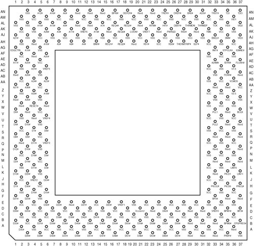 The last versions of the Pentium III use the Tualatin core design, which requires a revised socket to operate. Motherboards that can handle Tualatin-core processors are sometimes known as Tualatin-ready and use different chipsets from those not designed to work with the Tualatin-core processor. If you need to replace a Pentium III processor on a Socket 370 server motherboard, make sure you determine what versions of the Pentium III the board can handle. See the vendor documentation for the system or motherboard for details. Tip The maximum speed of the Tualatin-core Pentium III processor is 1.4GHz. Some vendors refer to their Tualatin-compatible motherboards as supporting up to 1.4GHz processors. Socket 423Socket 423 is a ZIF-type socket introduced in late 2000 for the original Pentium 4. Figure 2.19 shows Socket 423. Figure 2.19. Socket 423 (Pentium 4) showing pin 1 location. Socket 423 supports a 400MHz processor bus, which connects the processor to the MCH, which is the main part of the motherboard chipset and similar to the North Bridge in earlier chipsets. Pentium 4 processors up to 2GHz were available for Socket 423; all faster versions of the Pentium 4 use Socket 478 or Socket 775 instead. Socket 423 uses a unique heatsink mounting method that requires standoffs attached either to the chassis or to a special plate that mounts underneath the motherboard. This was designed to support the weight of the larger heatsinks required for the Pentium 4. Because of this, many Socket 423 motherboards require a special chassis that has the necessary additional standoffs installed. Fortunately, the need for these standoffs was eliminated with the newer Socket 478 and Socket 775 for Pentium 4 processors. The processor uses five VID pins to signal the voltage regulator module (VRM) built in to the motherboard to deliver the correct voltage for the particular CPU installed. This makes the voltage selection completely automatic and foolproof. Most Pentium 4 processors for Socket 423 require 1.7V. A small triangular mark indicates the pin-1 corner for proper orientation of the chip. Socket 478Socket 478 is a ZIF-type socket for the Pentium 4 introduced in late 2001. It was specially designed to support additional pins for future Pentium 4 processors and speeds over 2GHz. The heatsink mounting is different from that of the Socket 423, allowing larger heatsinks to be attached to the CPU. Figure 2.20 shows Socket 478. Figure 2.20. Socket 478 (Pentium 4) showing pin 1 location. Socket 478 supports a 400MHz, 533MHz, 800MHz, or 1066MHz processor bus that connects the processor to the MCH, which is the main part of the motherboard chipset. Socket 478 uses a different heatsink attachment method than its predecessors. Socket 478 uses a heatsink that clips directly to the motherboard, and not the CPU socket or chassis (as with Socket 423 and Socket 370). Therefore, any standard chassis can be used, and the special standoffs used by Socket 423 boards are not required. The new heatsink attachment allows for a much greater clamping load between the heatsink and processor, which aids cooling. Socket 478 processors use five VID pins to signal the VRM built in to the motherboard to deliver the correct voltage for the particular CPU installed. This makes the voltage selection completely automatic and foolproof. A small triangular mark indicates the pin-1 corner for proper orientation of the chip. Socket 603 and Socket 604The Intel Xeon is based on the Pentium 4, but it supports larger amounts of on-die L2 cache. Some versions contain L3 cache. Socket 603 is used with the Intel Xeon processor in DP (dual-processor) and MP (multiple-processor) configurations. The additional pins in Socket 603 provide support for DP or MP operation at a processor bus speed of 400MHz. Figure 2.21 shows Socket 603. Figure 2.21. Socket 603 is used by the Intel Xeon processor. Socket 604 is a variation on Socket 603, using an additional pin at location AE30. Socket 604 supports newer Xeon MP and DP processors with processor bus speeds up to 800MHz. The additional pin on Socket 604 processors prevents them from being inserted into a Socket 603 motherboard. Socket 775 (Socket T)The most recent Intel Pentium 4 processors as well as the Pentium D and Pentium Extreme Edition use a new processor socket called Socket 775 (LGA775). Originally known as Socket T, Socket 775 is unique among x86 sockets in that it uses an LGA format, so the pins are on the socket rather than the processor (see Figure 2.22). The first LGA processors were the Pentium II and Celeron processors in 1997; in those processors, LGA packaging was used for the chip mounted on the Slot 1 cartridge. Figure 2.22. Socket 775 (LGA775, Socket T) and its processor clamping mechanism.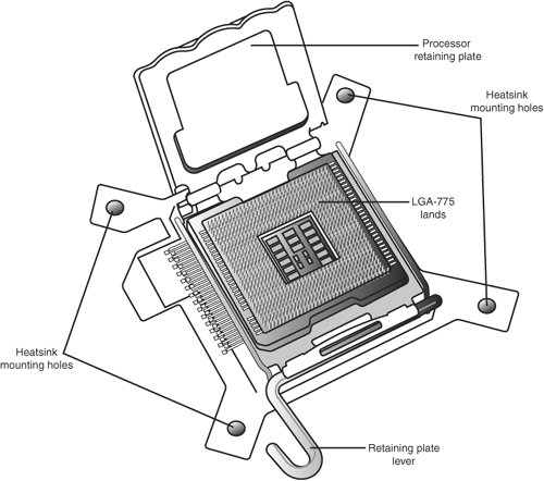 LGA is really just a recycled version of what was previously called LCC (leadless chip carrier) packaging. Used way back on the 286 processor in 1984, LCC packaging had gold lands around the edge only (there were far fewer pins back then). In other ways, LGA is simply a modified version of BGA, with gold lands replacing the solder balls, making it more suitable for socketed (rather than soldered) applications. The early LCC packages were ceramic, whereas the first Pentium II LGA packages were plastic, with the package soldered to a cartridge substrate. These days (and for the future), the LGA package is organic and directly socketed instead. On a technical level, the Pentium 4 LGA chips combine several packaging technologies that have all been used in the past, including organic LGA (OLGA) for the substrate and controlled collapse chip connection (C4) flip-chip for the actual processor die. Socket A (Socket 462)AMD introduced Socket A, also called Socket 462, in 2000 to support the PGA versions of the Athlon and Duron processors; it also works with the Athlon XP and Athlon MP processors. Socket A has 462 pins and 11 plugs oriented in an SPGA form (see Figure 2.23). Socket A has the same physical dimensions and layout as Socket 370; however, the location and placement of the plugs prevent Socket 370 processors from being inserted. Socket A supports 32 voltage levels from 1.100V to 1.850V, in 0.025V increments, controlled by the VID0 to VID4 pins on the processor. The automatic VRM circuitry is typically embedded on the motherboard. Figure 2.23. Socket A (Socket 462) Athlon/Duron layout. There are 11 total plugged holes, including 2 of the outside pin holes at A1 and AN1. These are used to allow for keying to force the proper orientation of the processor in the socket. The pinout of Socket A is shown in Figure 2.24. Figure 2.24. Socket A (Socket 462) pinout (top view). Socket 939The AMD Opteron processor was introduced using Socket 940 (discussed in the next section), and most versions of the Opteron continue to use Socket 940. However, starting in 2005, AMD introduced a wide variety of 100-series Opterons in Socket 939. Figure 2.25 illustrates Socket 939. Figure 2.25. Socket 939. The cutout corner and triangle at the lower left indicate pin 1. Socket 939, unlike Socket 940, supports standard unbuffered DDR memory. Because unbuffered DDR memory is less expensive than the registered memory used by Socket 940 versions of the Opteron, Socket 939 Opterons enable you to build a lower-cost single-processor server than do Socket 940 versions. However, note that 100-series Opterons are designed to work in single-processor configurations only. If you are planning to build a two-way or larger configuration, you must use 200-series (up to two-way) or 800-series (up to eight-way) processors, which are available only in Socket 940. Socket 940Socket 940 (see Figure 2.26) is used by most versions of the AMD Opteron, including all versions designed for two-way or larger configurations (200 and 800 series). Motherboards that use this socket support only registered DDR SDRAM modules in dual-channel mode. Figure 2.26. Socket 940. The cutout corner and triangle at the lower left indicate pin 1. When you compare the pinouts for Sockets 939 and 940, note that the areas without pins are different. This keying prevents you from inserting the wrong processor into the motherboard. Both Socket 939 and Socket 940 use heatsinks that clip to a frame rather than directly to the processor socket. This enables easier heatsink installation. Pin Array Cartridge (PAC)The original Itanium used a package called the pin array cartridge (PAC). This cartridge includes L3 cache and plugs in to a PAC418 (418-pin) socket on the motherboard and not a slot. The package is about the size of a standard index card, weighs about 6 ounces (170g), and has an alloy metal on its base to dissipate the heat (see Figure 2.27). Itanium has clips on its sides, enabling four PACs to be hung from a motherboard, both below and above. Figure 2.27. The Itanium's PAC. The Itanium 2 uses a more compact version of the PAC, known as PAC611. See Figure 2.28. Figure 2.28. The Itanium 2 has a more compact design than the original Itanium. (Photograph used by permission of Intel Corporation.) The Itanium and Itanium 2 processors both use a unique power source known as a "power pod" (see Figure 2.29). The processor slides into the edge connector on the power pod. The power pod acts as a voltage regulator (sometimes referred to as a DC/DC converter) to provide the correct power levels and power quality to the processor and its onboard cache memory. The power pod uses VID pins to specify the correct voltage for the processor. Note that the Itanium's power pod is not compatible with the Itanium 2's and vice versa. Figure 2.29. A typical power pod for the Itanium 2 processor. A power pod for each processor socket is usually supplied with an Itanium 2 motherboard or server. If you need replacements, you should contact your motherboard or server vendor. | ||||||||||||||||||||||||||||||||||||||||||||||||||||||||||||||||||||||||||||||||||||||||||||||||||||||||||||||||||||||||||||||||||||||||||||||||
EAN: 2147483647
Pages: 240