Link Initialization
| The process of initializing each link begins during cold reset. The complete link initialization process consists of several stages:
Low-Level Link Width InitializationLow-Level initialization of the link width is performed as a hardware sequenced point-to-point handshake between the two devices attached to each link. Once completed, the devices at each end of the link will be ready to perform transactions using either 2-, 4-, or 8-bits. This link-width negotiation sequence may not result in links operating at their maximum width. For example, since the maximum width following the negotiation is 8 bits, 16-bit, 32-bit, and asymmetrically - sized operations are not possible until enabled by software, which is the second stage of link-width initialization. Determining Low-Level Link WidthHT permits devices with different link widths to be directly connected. This results in unused receiver and transmitter pins on the wider device. Logic within a device of course has no knowledge of the width of devices to which it connects. Consequently, a hardware handshake process is defined at powerup to ensure that all devices can determine a safe link width over which devices can communicate. During reset all devices drive a pattern onto the link(s) to which they connect. This pattern defines the width of the transmitting device's receiver. (See Table 12-1 on page 283) The value received by each device defines the width at which they will communicate following cold reset. While this negotiated width may not be optimized for best performance, this method ensures that all devices can communicate safely. Subsequently, firmware-driven link width initialization maximizes the link width. (See "Tuning the Link Width (Firmware Initialization)" on page 295). Table 12-1. Transmitter Value Driven to Indicate Receiver Width
Comments regarding Table 12-1 on page 283:
The CAD values received during low-level initialization are interpreted by the device as shown in Table 12-2 on page 284. Table 12-2. Interpretation of Value Received on the CAD Lines to Determine Receiver Width
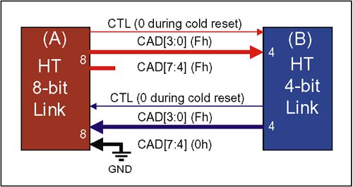
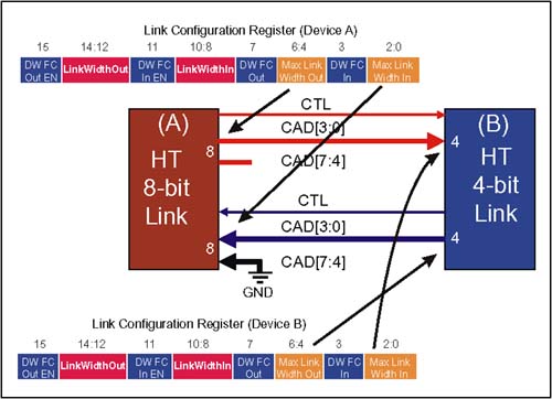
The following examples are offered to clarify the low-level receiver width detection process with different transmitter and receiver sizes. Patterns that represent 16- and 32-bit link widths are not supported by this low-level initialization process. Example 1: 4-bit device connected to 8-bit DeviceRefer to Figure 12-6 on page 285 during the following discussion. In this example an HT device with a 4-bit receiver and transmitter is connected to an HT device with an 8-bit receiver and transmitter. The specification requires that receivers that are wider than the transmitters to which they connect must connect the unused receiver inputs to logical zero as illustrated in Figure 12-6. This prevents the inputs from floating. Also, since the 8-bit device's transmitter connects to a 4-bit receiver, the upper four transmitter pins (CAD 7:4) are not connected. Figure 12-6. Low-Level Link Width, Example 1 During reset both devices deliver a pattern that represents the size of their receiver according to Table 12-1 on page 283, as follows :
The receivers then detect the pattern driven, and each device learns the link width to use when transmitting packets to the other.
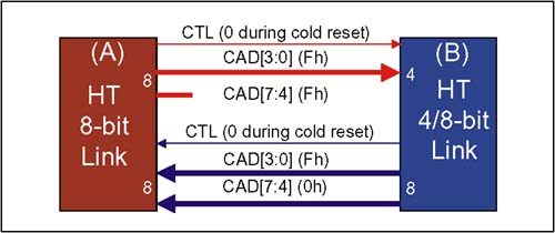
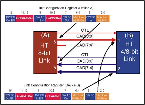
Example 2: 8-Bit Device Connected to 4/8-Bit DeviceRefer to Figure 12-7 on page 286 during the following discussion. Device A with 8-bit transmitter and receiver is connected to device B with a 4-bit receiver and 8-bit transmitter. The 8-bit transmitter of device B connects to the 8-bit receiver of device A, and the 8-bit transmitter of device A connects to the 4-bit receiver of device B. CAD [7:4] of A's transmitter are not connected, because the receiver in device B is only 4-bits wide (CAD[3:0]). Figure 12-7. Low-Level Link Width, Example 2 During reset both devices deliver a pattern that represents the size of their receiver according to Table 12-1 on page 283, as follows:
The receivers then detect the pattern driven, and each device learns the link with to use when transmitting packets to the remote device.
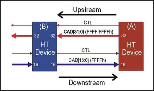
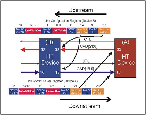
Example 3: 32-bit Upstream and 16-bit DownstreamBoth devices attached to this link in this example support 16-bit widths in the downstream direction and 32-bit widths in the upstream direction. During reset both devices deliver a pattern that represents the size of their receiver according to Table 12-1 on page 283, as follows:
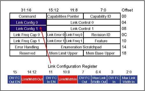
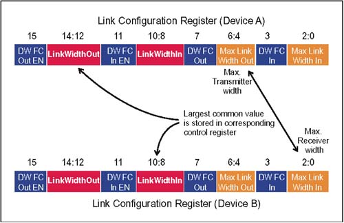
Because the pattern delivered in both cases represents receivers wider than the minimum 8-bit width supported during low-level initialization, the receivers interpret the values as the maximum width (8-bits). Note that this low-level method of defining the link width to use following cold reset always results in the same width being used for both upstream and downstream transfers. Figure 12-8. Low-Level Link Width, Example 3 Negotiated Link Width Stored in Link Config RegistersWhen the low-level link initialization process has completed, each device updates its HT Link Configuration register to reflect the negotiated link width. Figure 12-9 illustrates the Link Configuration register and the link-width fields that are updated to reflect the negotiated width of the link. Two link configuration registers are defined:
Figure 12-9. Link Configuration Register Each of these registers contains two fields that define the link width used for the transmit and receive connections of the link. These 3-bit fields are named LinkWidthIn and LinkWidthOut. The low-level link width value loaded into these registers following cold reset becomes the default value and will always be the same for LinkWidthIn and LinkWidthOut. These fields may be updated later by software to reflect the optimum link width. Table 12-3 on page 289 lists the encoded link-width values. Table 12-3. Encoded Link-Width Values used in the Link Configuration Registers
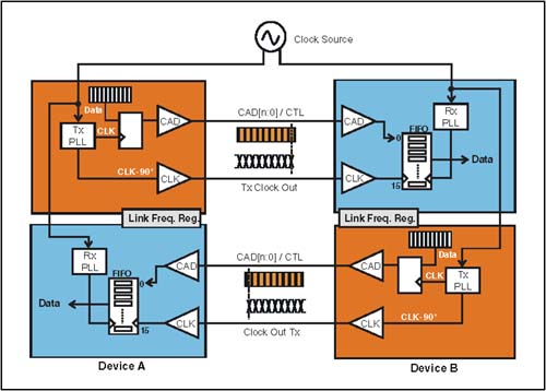
Low-Level Clock InitializationHT devices use a transmit clock (Tx Clk) to clock out a packet from the transmitter interface and a receive clock (Rx Clk) to receive an incoming packet. Figure 12-10 illustrates the relationship between the transmit and receive clock between two devices A and B. Device A transmits (upper half of link) a packet from the transmit FIFO to device B which receives the packet in the receiver FIFO. Similarly device B transmits (lower half of link) a packet from the transmit FIFO to device A which receives it in the receiver FIFO. Figure 12-10. Link Interface and Clocking In a receiver device, the load pointer which is synchronous to Tx Clock Out (transmit time domain) points to the location within the receive FIFO where the incoming packets are stored. The unload pointer which is synchronous to Rx Clk (receiver time domain) points to the location from which data in the receive FIFO is unloaded into the core logic. The multiplexer sizes the data path width of the FIFO appropriately to match the data path width of the core logic. The clock source supplies a clock to both devices. In this example, the clock source (source PLL) feeds the transmit and receive PLLs of both devices. A packet is clocked out synchronously to Tx Clk generated by the Transmit PLLs. The transmit PLLs also generates the Tx Clock Out signal that is visible on the link. Tx Clock Out lags Tx Clk by 90 degrees to center the clock transition within the bit time. CAD[n:0]/CTL data is loaded into the receive FIFO using Tx Clock Out clock received at a receiver device. Data is unloaded from the receive FIFO into the core logic using Rx Clk generated by the receive PLLs. For additional detail regarding clock and FIFO initialization refer to Chapter 15, entitled "Clocking," on page 387. The Default Clock FrequencyFollowing cold reset all HyperTransport I/O link transmitter and receivers must operate at the default HyperTransport clock frequency of 200 MHz. Cold reset initializes HyperTransport I/O link transmitters to this default link clock frequency. Control and CAD Sequence after Reset is RemovedFollowing the deassertion of RESET#, the CTL and CAD signals go through a series of transitions that trigger various stages of low-level link initialization. These transitions and the related initialization events are listed in Table 12-4 on page 291 and detailed in the following sections. Table 12-4. CTL/CAD Sequence Following Deassertion of RESET#
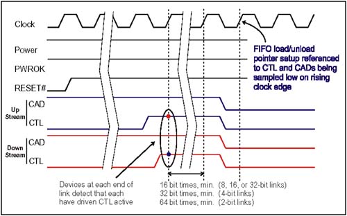
Clock Synchronization (CTL=0 & CAD=0)Variation between the transmit clock and receive clocks can cause underrun or overrun without the appropriate FIFO size and load and unload pointer values. These pointers must be set up prior to beginning packet transmission and are triggered by CTL and CAD transition from high to low. Details regarding clock initialization, including FIFO size and separation between the FIFO write and read pointers, can be found in Chapter 15, entitled "Clocking," on page 387. Figure 12-11 on page 293 illustrates the initialization sequence and the point at which the receive FIFO setup is referenced. To simplify the illustration, a single clock is illustrated rather than the multiple source synchronous clocks actually implemented. The specification defines the FIFO load and unload pointer setup as follows:
Figure 12-11. Clock Synchronization and FIFO Load and Unload Pointer Setup Note that the point at which the pointers are set up may be different between the downstream and upstream transmitters and receivers. Figure 12-11 on page 293 depicts a link interface and the CTL and CAD timing associated with FIFO pointer setup. This example presumes that the link is symmetrical (i.e. 8-bits wide in both directions). Note also that the transitions of the CTL and CAD signals are shown transitioning from high to low at the same for both directions; however, this may not always be the case. Figure 12-11 illustrates the point at which the devices at each end of the link detect that the other has asserted CTL on a rising clock edge. From this point a minimum delay must be honored before each device deasserts its CTL and CAD lines:
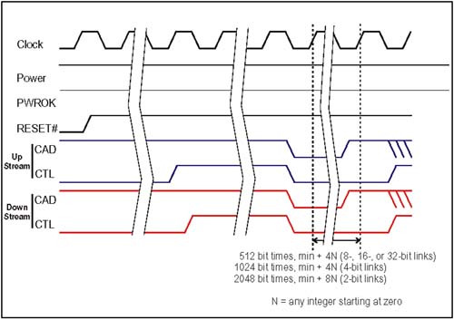
Because these timing parameters are specified as minimum values, the devices at each end of the link may implement different delays. The example shows both devices deasserting CTL and CAD at the same time, indicating that they use the same delay. The delay is extended when LDTSTOP# is asserted (>50 m s) to permit time for devices to recover from a link power-down condition. (See "LDTSTOP# Disconnect Sequence" on page 304 for details). Duration of CTL & CAD Driven LowCTL and CAD remain low for a specified minimum duration depending on CAD width as listed below and as illustrated in Figure 12-12:
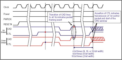
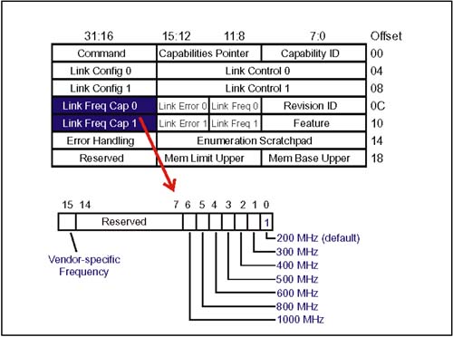
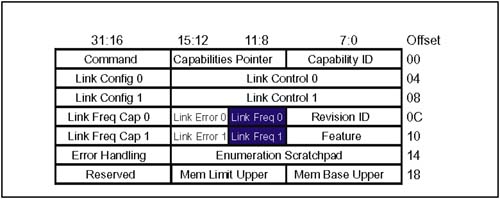
Figure 12-12. Duration of CTL & CAD Deassertion These values ensure that the next transition is equivalent to a 4-byte boundary, and from this point, all transitions of CTL or the CAD lines must occur on 4-byte boundaries until the end of Cold RESET. Packet Framing and Initializing the CRC WindowOnce the low-level link width is determined, the transmitter and receiver pair that is used for a given direction must be synchronized as they begin packet transmission and reception . Note that each direction of the link must perform this synchronization but that they are independent of each other. This reference point specifies the alignment of packets on a 4-byte boundary, as well as the beginning of the CRC window. CRC generation is based on 512-byte intervals that begin at the end of low-level initialization on each link. Figure 12-13 on page 295 illustrates the Reset timing that "frames" packets on 4-byte boundaries and initiates packet transmission and the beginning of the CRC window. Each device drives the CAD signals to a logic 1 across a rising CLK edge for exactly four bit-times, while leaving the CTL signal deasserted. The transition from all CAD signals deasserted to all CAD signals asserted serves to frame incoming packets. The first bit-time after these four must have CTL asserted, and is both the first bit-time of a new command packet and the first bit-time of the first CRC window. It also occurs across a rising CLK edge. Figure 12-13. Framing and CRC Window Sequence As a reminder, the examples presented above show the CTL and CAD transitions occurring at the same time for both directions of the link. However, after the receivers detect that the other has asserted its CTL signal, the synchronization for each direction of the link is independent. Once low-level initialization is complete, the Initialization Complete bit in each active Link Control register is set. Tuning the Link Width (Firmware Initialization)Low-level link width negotiation does not guarantee that the maximum link width is used following cold reset. Therefore, system firmware or perhaps the O.S. must check the link width capability of devices at ends of each link to determine if the maximum possible link width is being used. As discussed in "Negotiated Link Width Stored in Link Config Registers" on page 288, the Link Configuration Register contains the LinkWidthIn and LinkWidthOut fields that control the actual width used by each device's receiver and transmitter. The default value after cold reset is the negotiated value, which is always the same for upstream and downstream transfers. Tuning the link width involves firmware that determines whether the devices attached to each link can operate at a width greater than the default setting. This is accomplished by reading the MaxLinkWidthIn and MaxLinkWidthOut fields. The largest common value for each transmitter/receiver pair is selected and stored in the corresponding LinkWidthIn and LinkWidthOut fields. Figure 12-14 on page 296 illustrates this process for one pair. Figure 12-14. Link Width Update When software makes changes to the LinkWidthIn and LinkWidthOut fields, the new values loaded into these fields have no immediate effect on link operation. The updated width values take effect only after warm reset (See "Warm Reset" on page 302) or a disconnect/reconnect sequence via the LDTSTOP# protocol (See "HT Link Disconnect/ Reconnect Sequence" on page 223). The following sections describe the result of link-width tuning on the previous low-level link width examples. Tuning Example 1: 4-bit device connected to 8-bit DeviceDuring the low-level link width process a default link width of 4 bits was established (for both directions). Figure 12-15 on page 297 shows that for each direction the maximum link values are 4 bits and 8 bits, thus the largest common width is 4 bits in each direction. In this example, software is unable to increase the link width beyond the negotiated width. Figure 12-15. Maximum Link Values, Example 1 Tuning Example 2: 8-bit device connected to 4/8-bit DeviceLow-level width determination in this example (described in "Example 2: 8-Bit Device Connected to 4/8-Bit Device" on page 285) results in a link width of 4 bits in both directions. A firmware check of the maximum link-width would reveal that the top portion of the link (see Figure 12-16 on page 298) can operate at a maximum width of 4 bits (the same as the negotiated width); however, the lower portion of the link has a transmitter and receiver that are both capable of transferring 8 bits at a time. Figure 12-16. Maximum Link Values, Example 2 Tuning Example 3: 32-bit Upstream and 16-bit DownstreamThe third example has devices with widths greater than 8 bits. Since the negotiated value was limited to 8 bits, tuning will result in far better performance than the low-level width negotiation. Figure 12-17 on page 299 illustrates that the maximum link width for the upstream link is 32 bits and the downstream link is 16 bits. Figure 12-17. Maximum Link Values, Example 3 Tuning the Clock FrequencyBecause the devices at the ends of each link may support a clock frequency higher than the default, initialization firmware reads the Link Frequency capability register to determine the highest common clock speed supported by the devices at each end of the link. The Frequency Capability Register is a member of the HT capability register set as illustrated in Figure 12-18 on page 300. This read-only register defines which clock frequencies a given HT device supports. Each bit corresponds to one of the specified clock frequencies, and Bit 0 must always be set to indicate support for 200 MHz operation. Note that two Frequency Capability registers (labeled Link Freq Cap 0 and 1) are defined in the capability registers to support devices such as tunnels that have two link interfaces to define. If a given device has a single link interface then only the first register is used. System firmware selects the highest common clock frequency supported by both devices connected by the link. Figure 12-18. Tunnel Example Link Frequency Capability Registers The maximum clock frequency supported is loaded into the Link Frequency register so that the link can run at the fastest speed. Figure 12-19 on page 301 illustrates the locations of the Link Frequency register within the HT capability register set, and Table 12-5 on page 301 shows the encoding for the different frequencies. Once the new maximum clock frequency value is loaded, system firmware must initiate a warm reset or LDTSTOP# disconnect sequence to invoke the changes to the link clock frequencies. Figure 12-19. Link Frequency Register Location within the HT Capability Register Set Table 12-5. Encodings for Link Frequency Field of Link Configuration Register
|
EAN: 2147483647
Pages: 182