Synchronous Clock Mode
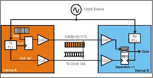
| The specification requires that all HT devices support the synchronous clock mode. This mode is the least complicated method of transferring data from transmitter to receiver. Synchronous clock mode requires that the transmit clock and receive clock have the same source, and operate at the same frequency. If we were to assume that the transmit clock and the receive clock always remained synchronized, then a simple clocking interface could be used as described in the following example. A Conceptual ExampleIn this synchronous example, the transmit clock (Tx Clock) and receive clock (Rx Clock) are presumed to be in synchronization. Note, however, that source synchronous clocking requires that Transmit Clock Out (Tx Clk Out) be 90 ° phase shifted from Tx Clock. In this example all other sources of transmit to receive clock variation are ignored, including the expected clock drift associated with PLLs. Refer to Figure 15-1 on page 390 during the following discussion. (Note that only one link direction is illustrated .) The transmitter delivers data synchronously across the link using the transmit clock. Tx Clock Out is sourced later and lags the data by 90 ° (or one-half bit time), thereby centering the clock edge in the middle of the valid data interval. When the data arrives at the receiver it is clocked into the FIFO using Tx Clock Out. Note that the clocked FIFO has two entries, which provides a separation of 1 between Tx Clock Out and Rx Clock. Data written into the FIFO during clock 1 would not be read from the FIFO using Rx Clock until clock 2. This one entry separation (called write-to-read separation) permits time for the sample to be stored prior to being read (i.e. the FIFO entry is not being written to and read from in the same clock cycle). In short, two FIFO entries are sufficient to provide the separation needed to ensure that data is safely stored and transferred into the receive clock domain. Figure 15-1. Simple Synchronous Clocking Interface However, in the real world many factors contribute to timing differences between the transmit and receive clock that are potentially significant, even though the clocks originate from the same source. These real world perturbations result in somewhat more complicated implementations that must account for and manage the worst case variation between the transmit and receive clocks. Specifically , the specification describes the receive FIFO implementation for handling the variation between the transmit and receive clocks. Sources of Transmit and Receive Clock VarianceThe specification defines and details the sources of transmit and receive clock variation that can exist. These clock differences can create FIFO overflow or underflow if not identified and taken into account. The clock differences can be attributed to two different categories or sources:
The sources of clock variation in some cases can accumulate over time, causing clock variation to increase over time. However, all of the sources of clock variation are naturally limited in terms of the maximum amount of change that can occur. For example, a PLL is designed to produce an output clock that is synchronized with the input source clock, but with certain limitations. That is, variation of output frequency is specified not to change beyond a certain phase shift. The time over which the clock phase may change can be relatively short or perhaps much longer depending upon conditions. The consideration and assessment of the sources of clock variance is done to determine a FIFO size that can absorb the worst-case clock variation. This would occur if all sources of clock variation simultaneously reach their extremes, a very unlikely circumstance. This chapter discusses the variant and invariant sources of transmit clock to receive clock variance. It also provides an example timing budget for each source. Invariant SourcesThe time-invariant factors contribute a small proportion of the overall clock variance. The invariant factors include:
Cross-byte skew in multi-byte link implementationsDifferences in the arrival of Tx Clock Out at the receiver (CLKIN) between each byte lane is caused by path length mismatch. This constant skew is termed T bytelaneconst in the specification. The specification allows up to 1000ps for this skew. Consequently, when multiple bytes are clocked into the FIFO the maximum skew could result in one of the bytes being clocked into the FIFO 1000ps later than the associated bytes. Thus, when the associated bytes are clocked out of the FIFO by Rx Clock, one byte having arrived late may be left behind. This problem is solved by adding additional entries in the FIFOs to handle the maximum lane-to-lane skew, ensuring that all associated bytes are clocked out at the same time. Note that lane-to-lane skew may change due to the effects of temperature, voltage change, etc. This parameter called T bytelanevar is included in the variant source list. Sampling ErrorUncertainty in read pointer due to CTL sampling error in the receive clock domain (1 device specific Rx Clock bit time). The specification does not specifically define the source of this sampling error, but is likely caused by phase variations between the Tx Clock Out and Rx Clock that could cause a sample to be missed. Adding an additional bit time solves this problem. Variant SourcesThe phase difference between the transmit and receive clock may change significantly due to dynamic factors such as:
All time variant parameters must be considered in terms of their worst-case variance. The total dynamic phase variation due to these factors is called T variant. Additionally, the transmit clock could either LEAD the receive clock by T variant or it could LAG the receive clock by T variant . Consequently, the receive FIFO must be sized to accommodate both phase variations. Reference Clock Distribution SkewSynchronous clock mode requires that the input reference clocks to the transmitter and receiver be derived from the same time base. The distribution of the reference clock to the transmitter and the receiver results in skew between the two reference clocks. This is due to:
This skew results in phase difference between the Transmit and Receive Clocks and must be included in the T variant calculation. PLL Variation in Transmitter and ReceiverThe largest contribution to the overall Tx Clock to Rx Clock variance comes from the PLLs. The PLL is constantly making adjustments to the output frequency as a result of a feedback loop. In addition, voltage and temperature changes also add to the possible output clock variation. The sample timing budget included within the specification allows a maximum PLL output phase variation of 3500ps. This represents >1 bit time at the 400 MT/s rate and approximately 5.6 bit times at the 1600MT/s rate. Transmitter and Link Transfer VariationThe transmitter clock error ( accumulated over a single bit time), the transmitter PHY, and the interconnect contribute small amounts of phase error into the link transfer clock domain through all of the parameters included in the link transfer timing. This includes noise on the PCB that affects both the clock and data in the same way causing a minor shift in frequency or phase of clock and data. (Note that if the noise affected the clock and data differently, this would affect the maximum bit transfer rate due to potential violations of T SU and T HD ). Receiver Transfer VariationThe receiver contributes small amounts of phase error in the received CLKIN due to distribution effects. Dynamic Cross Byte-Lane VariationThe specification also defines the dynamic components of the byte-land variation due primarily to temperature and voltage changes (T bytelanevar ). The static elements of byte-lane variation are discussed in "Cross-byte skew in multi-byte link implementations." on page 391. An Example Timing BudgetThe specification includes an example timing budget for the identified sources of clock variation. Table 15-1 on page 393 is duplicated from the specification and lists the timing values for transfer rates ranging from 200 to 1600MT/s. Table 15-1. Timing Variance Budget from Specification for Source of Clock Variation
Clock Variance, FIFO Size, and the Read PointerThis section discusses the relationships between the worst-case clock variance calculation, minimum FIFO size, and unload pointer initialization for synchronous clock mode. The following example is provided to help explain these relationships. (Also, see Figure 15-2 on page 394.) Figure 15-2. Synchronous Clock Example, Single Direction The following assumptions are made for this synchronous clocking mode example:
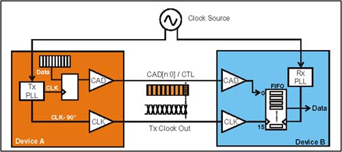
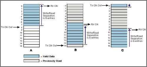
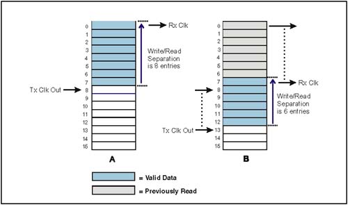
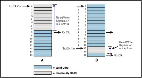
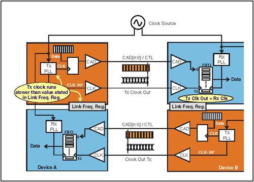
Minimum FIFO SizeRecall that the FIFO depth must be large enough to store all transmitted data until it has been safely read into the receive clock domain. The minimum FIFO size must account for the total possible variation between Tx Out Clock and Rx Clock. Note the T variant parameter must be doubled because Tx Clock Out may either lead or lag Rx Clock by the time variant values. Therefore, the maximum phase shift is calculated as: T variant * 2 = T total variant The variance numbers in this example yield the following T total variant value: 8,390ps * 2 = 16,780ps The minimum FIFO size can be calculated by dividing the total clock variation time by the bit time duration. ((T variant * 2) + T invariant ) Bit time = FIFO Entries For this example, the number of FIFO entries is: ((8,390ps * 2) + 2,500ps) 1250ps = 15.4 FIFO Entries The number of entries is rounded up to the next integer value, or 16 in this example. Note also that this computation of minimum FIFO entries is different from the results shown in Table 15-1 on page 393 from the specification. The reason for the smaller FIFO size is that this example implementation does not have multiple byte lanes , therefore the T bytelanevar and T bytelaneconst parameters are not included in the worst-case clock variation. Write-to-Read and Read-to-Write SeparationRecall that the FIFO depth must be large enough to store all transmitted data until it has been safely read into the receive clock domain. The separation from the write pointer location where data is written and the read pointer location from which data is read must be large enough to ensure the FIFO location can be read safely into the receive clock domain. To accommodate this clock variance in this example, the read pointer within the FIFO would need to be separated from the write pointer by 8 entries (or, bit times). The following three scenarios are provided to explain the operation of the FIFO and its pointers. Scenario 1: Tx Out Clock and Rx Clock are in SyncIn this example, the clock variation happens to be zero, with the specified separation between the write and read pointers set to 8 entries as calculated above. Figure 15-3 on page 396 illustrates the position of the pointers as a progression (labeled Stages A, B, and C). Note that the write pointer is labeled as Tx Clock Out to remind us that data is written using the transmit clock. For the same reason, the read pointer is labeled as Rx Clock. Figure 15-3. FIFO Operation When Tx Clock Out and Rx Clock are in Sync Stage A ” the write pointer has progressed from entry 0 to entry 8. Because the separation between the write and read pointer is 8, Rx Clock is prevented from clocking data from the FIFO until the separation reaches 8. At this stage, the separation has just been reached, so Rx Clock clocks data from entry 0, while the Tx Clock Out clocks data into entry 8. Stage B ” the write pointer has progressed to entry 15 and because there is still no phase difference between Tx Clock Out and Rx Clock the separation between the pointers remains at 8. Rx Clock is clocking data from entry 7 as Tx Clock Out is clocking data into entry 15. Stage C ” the write pointer has rolled from entry 15 back to entry 0 while the read pointer has advanced to entry 8. This simply illustrates that the separation is still maintained when the write pointer reaches the end of the FIFO and wraps back to entry 0. Scenario 2: Tx Clock Out Lags Rx ClockThis scenario shows the effects of the Tx Clock Out lagging the Rx Clock. The amount change in phase shift between the clocks as illustrated in Figure 15-4 on page 397 is dramatic. The amount of change illustrated would not likely have accumulated over such a small number of clocks; however, this amount of change could easily accumulate over a long interval. Figure 15-4. Effects of Tx Out Clock Lagging Rx Clock Stage A ” Stage A illustrates an initial write-to-read separation of 8, with the write pointer having progressed from entry 0 to entry 8. The Rx Clock clocks data from entry 0, while the Tx Clock Out clocks data into entry 8. Stage B ” Due to accumulated phase shift between Tx Clock Out and Rx Clock, Tx Clock Out now lags Rx Clock. This phase shift could be caused by phase changes in Tx Clock Out, phase changes in Rx Clock or a combination of both (if the event that the phase shift occurred in opposite directions). In this example, the write pointer has progressed to entry 13 but the read pointer has advanced more quickly to entry 7. Due to the accumulated phase difference between the transmit and receive clocks, the write-to-read separation has diminished to 6 entries. The FIFO was sized to 16 to absorb the maximum clock variation in the direction of Tx Clock Out lagging Rx clock. The maximum write-to-read separation of 8 in this example ensures the read pointer will not overtake the write pointer, which would result in FIFO underflow. Scenario 3: Rx Clock Lags Tx Clock OutThis scenario presents the opposite condition that was illustrated in scenario 2. In this example, the receive clock lags the transmit clock. As in the previous example, the phase difference between the clocks would not likely accumulate so quickly. Stage A ” the write pointer has previously traversed all of the entries and is back at entry 0 again, while the read pointer is at entry 8 This scenario focuses on the possibility that the Rx Clock lags the Tx Clock Out clock. In this case, the read-to-write separation becomes critical. In stage A this separation is 8. Stage B ” the write pointer has advanced to entry 13, while the read pointer has only advanced to entry 15. The write pointer had moved ahead by 13 entries and the read pointer has moved only 7 entries, leaving a read-to-write separation of only 2. Once again, the large change in clock variance over such a short period of time as illustrated in stage B would not occur. But the example does serve to illustration that over time the clock variance can accumulate and that an appropriately sized FIFO will be able to absorb the clock variance without overflow. Figure 15-5. Effects of Rx Clock Lagging Tx Clock Out Buffering Width and Speed DifferencesFIFOs may also provide buffering between a narrow high-speed link and a wider slower data path inside a receiver. CAD/CTL synchronization time:As discussed in "Clock Synchronization (CTL=0 & CAD=0)" on page 292, the read (unload) pointer of the FIFO for byte lane zero is established during initialization when the CAD and CTL signals are sampled deasserted in the receive clock domain. Since sampling the initial CTL and CAD signals in the receive clock domain will have some synchronization delay, this device-specific synchronization delay should be removed from the initial read pointer. Pseudo-Synchronous Clock ModeIn pseudo-synchronous mode, both Rx Clk in the receiver device and Tx Clk in the transmitter device are generated from the same time base clock just as in the synchronous mode case. During initialization, software configures each link to the maximum common frequency based on the values reported in each device's frequency capability register. The highest frequency supported by both devices is loaded into the Link Frequency register of each device. This value defines the highest frequency that both devices can use when sending packets over the link. In synchronous implementations this would be the exact frequency used by both devices. However, a device implementing pseudo-synchronous mode may arbitrarily lower the transmit clock frequency (Tx Clk or Tx Clock Out) below that specified by the Link Frequency register. Note that the receiver clock (Rx Clk) still runs at the frequency specified by the Link Frequency register. Figure 15-6 on page 400 illustrates an example implementation in which Device A lowers its Tx Clock frequency below the value specified in its Link Frequency register. Consequently, Device B stores data in its FIFO at a lower frequency than it removes data from the FIFO. Figure 15-6. Example Pseudo-Synchronous Mode Implementation Why Use Pseudo-Synchronous Clock Mode?The specification does not address any specific application for Pseudo-Synchronous clock mode. It appears that the main advantage is that a link is given the ability to transfer data in one direction at a higher rate than the other. But this begs the question, "Why not transfer in both directions at the highest speed possible, thereby keeping bus efficiency as high as possible?" It further raises the question of a possible advantage associated with clocking one direction at a slower rate; however, there would be power savings, reduced EMI, and reduced transmit PHY complexity. Implementation IssuesPseudo-synchronous clocking mode must take into account the same clock variance issued as synchronous mode. Additionally, several other key issues must be considered for pseudo-synchronous clocking mode. These issues include:
Methods and ProceduresThe specification does not define a mechanism to lower the transmit clock frequency, nor does it provide a method for determining which clock modes are supported by a given HT device. The specification states that:
Further, no definition exists regarding the level of software that would be involved in transitioning a device to the pseudo-sync mode. FIFO ManagementPseudo-sync mode must consider the same sources of clock variation as in synchronous mode and the receive FIFOs must be sized appropriately and the separation between the write and read pointers must be established. Because Tx Clock Out may run slower than Rx Clk in pseudo-synchronous mode, incoming packets may be clocked into the receive FIFO more slowly than they are clocked out. This situation results in a buffer underrun condition. To prevent this from happening the unload pointer occasionally must be stopped and then restarted when sufficient data is present in the receive FIFO. One approach to solving the potential underrun problem is to implement the FIFO to set a flag when the read pointer reaches the write pointer. The unload pointer could be stopped to keep additional reads from occurring until the situation is corrected. When sufficient separation between the load and unload pointers have accumulated, the flag can be cleared and reads can continue. Is Support for Pseudo-Sync Mode Required?The HT specification clearly requires support for synchronous clocking mode for all devices. It further states that:
This statement suggests that Pseudo-sync mode is conditionally required; that is, it's optional unless a device has some special conditions that require the support. Further, the specification does not mention any requirement for standard synchronous devices to operate correctly when attached to devices that operate in pseudo-sync mode. It may be that it is expected that all synchronous clocking mode devices will be able to inter-operate with pseudo-sync devices. As discussed in the previous section, support for pseudo-sync mode at the receiving end simply requires that the FIFO read pointer not be allowed to advance to the same entry as the write pointer. Asynchronous Clock ModeThe asynchronous clock mode permits the transmit and receive clocks to be derived from different sources. The specification limits the maximum difference permitted between the transmit and receive clock frequency. In this case, either the transmit clock or the receive clock may run faster than the other. So, both situations must be taken into account. Transmit Clock Slower Than Receive ClockIn this case, a potential underrun condition can develop. The solution for preventing underrun is the same as that discussed for the pseudo-synchronous clock mode as discussed in "FIFO Management." on page 401. In summary, the FIFO read pointer is prevented from reaching the write pointer by stopping the read clock until the transmit clock has had a chance to catch up. Transmit Clock Faster Than Receive ClockTx Clock Out can run slightly faster than Rx Clk in asynchronous mode (but by no more than 2000 ppm), thus incoming packets may be clocked into the receive FIFO faster than they are clocked out. This situation will result in a buffer overrun condition, and the receiver has no way of stopping or slowing the incoming packets. The following discussion describes how to prevent the buffer overrun condition from occurring. CRC bits appear on the link for 4 bit-times (on 8-,16-, and 32-bit links) after every 512 bit-times. These CRC bits are detected by the receiver, but NOT clocked into the receive FIFO. Instead the CRC bits are routed into the CRC error checking logic. Consequently, the FIFO write pointer does not increment during the CRC bit times, but the read pointer continues to increment and data continues to be read from the FIFO. As a result, the unload pointer has sufficient time to catch-up by clock data in the receive FIFO out before the buffer overruns. |
EAN: 2147483647
Pages: 182
- ERP Systems Impact on Organizations
- Challenging the Unpredictable: Changeable Order Management Systems
- Enterprise Application Integration: New Solutions for a Solved Problem or a Challenging Research Field?
- Context Management of ERP Processes in Virtual Communities
- Data Mining for Business Process Reengineering