7.3 A CMOS VCO architecture suitable for sub-1 volt GHz-range applications
|
7.3 A CMOS VCO architecture suitable for sub-1 volt GHz-range applications
Another key and critical building block in both wireless and optical communications transceivers is the voltage controlled oscillator (VCO). The continuous increase in the operating frequencies of integrated circuits, driven by the need for wider bandwidths and higher data rates, and the quest for system-on-chip solutions, resulted in a remarkable growth of interest in fully-integrated LC-based CMOS VCOs in recent years (e.g. [7, 10–12, 27–32]). Oscillating frequencies as high as 12.5 GHz have been achieved using standard digital CMOS processes, e.g. [7, 12, 32]. The structure of those VCOs employed stacked PMOS and NMOS transistors sharing the same DC current (Figure 7.17a), and therefore requiring relatively high supply voltages (2.5–3.5 V). Driven by the reduction of the power consumption of digital circuits and the scaling of modern technologies, the supply voltages of integrated circuits continue to decrease towards sub-1 V. New circuit architectures are needed, especially for analogue signal processors, to cope with this trend [33].
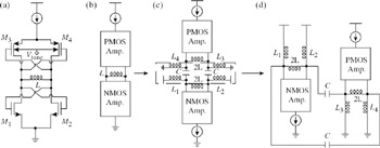
Figure 7.17: (a) Complementary differential LC VCO structure [12]; (b)–(d) progression towards a low-voltage topology
The VCO topology proposed in this section considerably reduces the supply voltage requirement, and consequently the power consumption. This is done by altering the structure of the conventional ‘complementary differential LC circuit’ shown in Figure 7.17a [12, 28]. In addition to maintaining the features of the original topology (discussed in Section 7.3.1), the proposed architecture provides an alternative to overcome the limited tuning range of back-gate tuning (Section 7.3.2). Detailed circuitry and design guidelines for the proposed topology are presented in Section 7.3.3.
Two VCO prototypes were implemented in a standard 0.18 μm CMOS process. They operate using 0.85 and 1 V power supplies, which is approximately one third the supply voltage needed by the original topology (labelled k and l in Figure 7.18). This is achieved while satisfying other requirements such as low phase noise, low power consumption (Figure 7.18), and a reasonable tuning range. Measured results are reported and discussed in detail in Section 7.3.4.
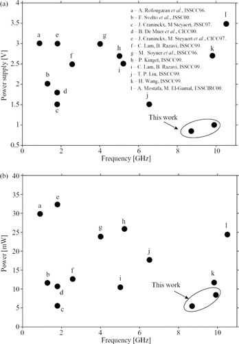
Figure 7.18: Comparison of supply voltage and power consumption versus frequency of state-of-the-art VCOs
7.3.1 The complementary differential LC structure
The complementary differential back-gate tuned VCO in Figure 7.17a has been shown to all owvery high frequencies of oscillation(9.8–12.5GHz)[5, 32]. It uses NMOS and PMOS cross-coupled amplifiers, along with a differential inductor L. The resonant tank is formed by the inductor and the parasitic capacitances of both amplifiers. Frequency tuning can be performed by controlling the PMOS transistors' back-gate voltages. This configuration has several desirable features:
-
The differential excitation of integrated inductors yields a higher effective quality factor [34]. This results in a decrease in the VCOs phase noise.
-
The PMOS devices are used for frequency tuning by controlling their back-gate voltages, thus eliminating the need for varactors which, as we have already discussed earlier, tend to degrade the tank quality factor at high frequencies.
-
Dispensing with the varactors allows for higher frequency of oscillation.
-
The tank resonator is formed in a loop configuration, i.e. none of its elements is referenced to ground (refer to Section 7.3.3.1 and Figure 7.20). This makes the frequency of oscillation less sensitive to transistors' and inductors' parasitics to the substrate.
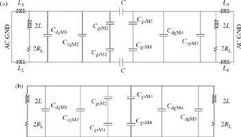
Figure 7.20: (a) Tank components for the circuit in Figure 7.19, and (b) high frequency equivalent circuit
The main drawbacks of the topology in Figure 7.17a are the relatively high voltage supply required, and the limited tuning range provided by back-gate tuning.
7.3.2 Proposed low-voltage VCO circuit architecture
The progression of the circuit structure towards a low-voltage topology is shown in Figure 7.17. Capacitors are inserted between the PMOS and NMOS sections to decouple their DC bias, without affecting the AC interaction between the two tanks. Inductors L1–L2 are then added to ensure a DC path from the power supply to the NMOS tank, while presenting a high impedance to the AC signals. Similarly, inductors L3–L4 secure a DC path for the PMOS tank to ground.
It is clear that the resulting topology significantly reduces the voltage supply required, while maintaining the characteristics of the original circuit. A second advantage is gained by decoupling the DC biasing of the two tanks. Tuning can now be done either using the back-gate voltage of the PMOS tank, or via its bias current. Combining both tuning mechanisms results in a wider tuning range (see Figure 7.23 on page 177).
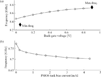
Figure 7.23: Frequency tuning versus (a) back-gate voltage, and (b) PMOS tank bias current. The two diamond points on the top figure show the minimum and maximum achievable frequencies, when both tuning schemes are combined
7.3.3 VCO detailed circuitry and design guidelines
Figure 7.19 shows the complete transistor-level VCO circuit. In the following subsections, we briefly highlight the main design issues related to the proposed structure.
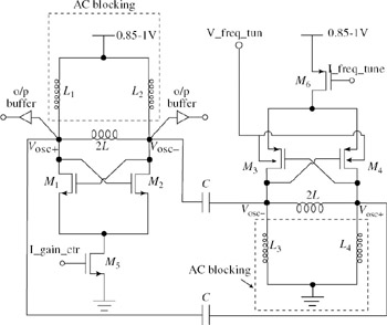
Figure 7.19: Circuit of the proposed VCO using capacitively coupled NMOS-PMOS LC tanks. The output buffers are on-chip PMOS transistors with 50 Ω resistor loads. V-freq-tun: Back-gate control voltage for frequency tuning. I-freq-tune: Bias-current control voltage for frequency tuning
7.3.3.1 The LC tank resonator
Figure 7.20a shows the AC equivalent circuit of the LC tanks of the VCO in Figure 7.19. It is composed of two differential inductors 2L, in parallel with a total capacitance composed of the drain–gate capacitances Cdg and gate–source capacitances Cgs of M1–M4. All the capacitances related to M1–M2 form the fixed component of the tank capacitance, whereas those of M3–M4 form the variable part. The design requirements of the DC-blocking capacitors C, and the AC blocking inductors L1–L4, are discussed in subsequent sections. In the high-frequency equivalent circuit shown in Figure 7.20b, the coupling capacitors are treated as short circuits, and L1–L4 as open circuits. The oscillator frequency is given by ![]() , where
, where
7.3.3.2 The coupling capacitors
The sizes of capacitors C need to be chosen to ensure they present a low-impedance path to the RF signal between the PMOS and NMOS tanks, at the frequency of oscillation. For this, the following condition needs to be satisfied
![]()
We used two 2.5 pF high-quality metal-insulator-metal (MIM) capacitors, which represent approximately 7–8 Ω of resistance at f0.
7.3.3.3 The AC-blocking inductors
The role of L1–L4 is to prevent the tank's energy from leaking to the voltage supplies. They should act as AC-blocking impedances. The impedance of each one of those inductors at f0, ZLblock, needs to be significantly larger than the tank impedance Ztank. It can be shown that this condition is ensured when the following relations are satisfied
![]()
![]()
In the prototypes presented here, each one of the blocking inductors is made up of a combination of an integrated spiral inductor in series with the bonding inductance of the package, with a total of approximately 3.5 nH.
7.3.4 VCO experimental results
A micrograph of the 8.7 GHz VCO chip is shown in Figure 7.21. Note that symmetry is conserved throughout the entire layout. All control nodes are bonded for packaging, while ground-signal-ground pads were used for on-chip probing of the RF output. The tank's coupling capacitors are built using the three top metal layers only, in order to avoid signal leakage to the substrate. Unit parallel capacitor cells were used to ensure good matching.
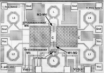
Figure 7.21: Micrograph of the 8.7 GHz VCO
The measured single-ended output spectra for the 8.7 and 10 GHz circuits are shown in Figure 7.22, and were used to directly estimate the phase noise. The latter are −86 dBc/Hz and −82 dBc/Hz at a 100 kHz offset for the 8.7 and 10 GHz VCOs, respectively. Note that the average power of the signal is underestimated due to the narrow span and limited resolution bandwidth of the spectrum analyser. In estimating the phase noise, the signal power was measured using a wider span [10].
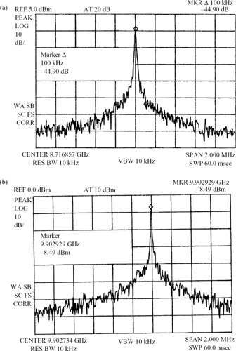
Figure 7.22: Measured single-ended outputs of the (a) 8.7 GHz and (b) 10 GHz VCOs
Two tuning mechanisms can be used to vary the VCO's frequencies. Figure 7.23a shows the frequency tuning using the back-gate voltages of the PMOS tank at a constant bias current of 2.36 mA. Figure 7.23b shows frequency tuning using the bias current of the PMOS tank at a constant back-gate voltage of 0.85 V. The two diamond points in the top figure show the minimum and maximum achievable frequencies, when both tuning approaches are combined. A maximum tuning range of 400 MHz is measured for the 8.7 GHz prototype, and 450 MHz for the 10 GHz.
One added advantage of the proposed topology is that the output amplitude is not very sensitive to the PMOS tank bias current, since the transconductance is mainly provided by the NMOS tank, while relatively lower current is used in the PMOS tank. Figure 7.24 shows the measured output power of the 8.7 GHz VCO as both the backgate voltage and bias current of the PMOS transistors are varied. The measurements indicate that as the PMOS tank bias current varies from 0 mA to 4 mA, the output power changes only by about 3.5 dBm, which can be a worthy trade-off for the increased tuning range. Table 7.2 summarises the characteristics and performance of the two VCO prototypes.
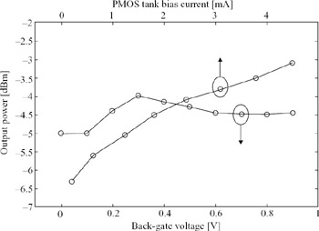
Figure 7.24: Output power variation of the 8.7 GHz VCO as a function of both the back-gate and bias current of the PMOS tank
| Prototype 1 [8.7 GHz] | Prototype 2 [10 GHz] | |
|---|---|---|
| | ||
| Technology | 0.18 μm, 6 metal | 0.18 μm, 6 metal |
| standard CMOS | standard CMOS | |
| Substrate resistivity | 10 Ω/cm | 10 Ω/cm |
| Thickness of top metal | 0.99 μm | 0.99 μm |
| Differential inductor | 1 nH | 0.85 nH |
| Estimated quality factor of inductor at f0 | 4 | 5 |
| Size of M1-M2 | 100 μm | 100 μm |
| Size of M3-M4 | 100 μm | 50 μm |
| Size of PMOS buffer | 50 μm | 50 μm |
| Chip area | 1.5mm 1.1mm | 1.5mm 1.1mm |
| Supply voltage | 0.85 V | 1 V |
| Supply current | 7.1 mA | 9 mA |
| Power consumption | 6.0 mW | 9 mW |
| Phase noise @ 100 kHz offset | −86 dBc/Hz | −82 dBc/Hz |
| Phase noise @ 600 kHz offset | −100 dBc/Hz | −98 dBc/Hz |
| Phase noise @ 1 MHz offset | −103 dBc/Hz | −101 dBc/Hz |
| Tuning range | 400 MHz | 450 MHz |
| Tuning sensitivity | 470.6 MHz/V | 450 MHz/V |
In order to fairly compare the overall performance of the VCOs presented here to that of state-of-the-art CMOS implementations operating at different frequencies and power levels, we make use of the following figure of merit (FOM) [35]
![]()
where fosc is the frequency of oscillation, Δf is the phase noise measured at an offset from fosc, and Pdissip is the DC power dissipation in the VCO. Equation (7.11) assumes a phase noise slope of 20 dB/decade, as suggested by Leeson's oscillator noise model [36]. A summary of the comparison result is shown in Figure 7.25. While achieving a very high frequency of oscillation at the lowest supply voltages, the FOMs of the two VCOs compare favourably to other implementations. Note that the signal power and phase noise of the VCOs labelled d and e in Figure 7.25 were measured differentially [28, 31], as opposed to the single-ended measurements of most of the other implementations. Note also that the VCO labelled k [12] requires more than 2.5 times the supply voltage of the VCOs reported here. Finally, a comparison of the tuning ranges to those of state-of-the-art implementations is given in Figure 7.26.
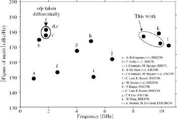
Figure 7.25: Comparison of the figure of merits of the VCOs presented in this work to that of state-of-the-art
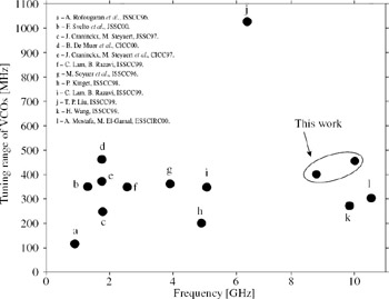
Figure 7.26: Comparison of proposed VCOs tuning ranges to state-of-the-art
|
EAN: 2147483647
Pages: 100
- Unicast IP Forwarding in Traditional IP Networks
- Cell-Mode MPLS
- Hierarchical VPLS-Distributed PE Architecture
- Command Reference
- Case Study 2: Implementing Multi-VRF CE, VRF Selection Using Source IP Address, VRF Selection Using Policy-Based Routing, NAT and HSRP Support in MPLS VPN, and Multicast VPN Support over Multi-VRF CE