7.2 A versatile low-voltage CMOS LNA topology
|
7.2 A versatile low-voltage CMOS LNA topology
The low noise amplifier is a critical building block in any RF receiver. It is usually the first active circuit in the received signal path. Its role is to amplify the weak input RF signal, while introducing as little noise as possible. Low noise figure, high linearity, enough gain, and low power consumption are the main performance merits of an LNA design.
With the targeted voltage supply down to 1 V, there is a limited number of suitable LNA topologies available to designers. Amplifier architectures which can operate from low voltage supplies are shown in Figure 7.1. Although the discussion in this chapter is mainly focused on the CMOS technology, some of the low-voltage topologies presented can be generalised to other technologies, such as silicon bipolar [16].
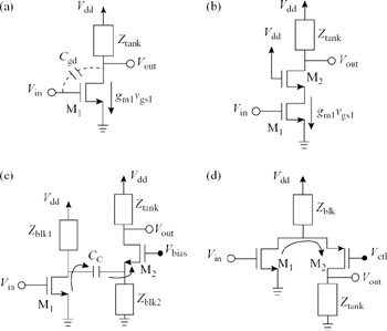
Figure 7.1: LNA topologies: (a) single transistor, (b) conventional cascode, (c) LC-coupled, (d) modified folded cascode
7.2.1 Single-transistor architecture
Consider the single-transistor amplifier shown in Figure 7.1a. Although the supply voltage can be made as low as the saturation voltage of the CMOS transistor, i.e. Vsat, the practical minimum supply voltage needed will have to be higher than the threshold voltage of the transistor necessary to properly bias it and to turn it on (Vgs>> Vth). In spite of meeting the very low supply requirement, there are many practical challenges with this circuit. Most importantly, this topology is very susceptible to instability problems, especially at RF. This is mainly due to the gate-to-drain parasitic capacitance (Cgd) which provides both forward and reverse low impedance paths between the input and output signals. This considerably complicates impedance and noise matching, since the input reactance is no longer dictated only by the gateto-source capacitance (Cgs), but is also dependent on a correlated function of the voltage gain (Av) and Cgd. The equivalent input capacitance of the transistor (Cin) is
described by
![]()
It should also be noted that this single-transistor structure suffers from the Miller effect, which limits its bandwidth.
7.2.2 Conventional cascode LNA architecture
In order to alleviate the limitations of the single-transistor LNA, it is very common to use the cascode configuration shown in Figure 7.1b. The main limitation of this structure is the need for a relatively high supply voltage headroom, since it involves the stacking of at least two transistors. This is not quite suitable for very low voltage applications. As the minimum feature sizes of the transistors are shrinking, the threshold voltage (Vth) and the drain-to-source voltage (Vds) are decreasing. It is therefore becoming more and more feasible to implement a low-voltage (i.e. <1V) cascode LNA in state-of-the-art deep-submicron technologies. However, the transistors will probably be forced to operate close to their triode mode, resulting in a serious degradation in linearity.
7.2.3 LC-coupled architecture
The need to improve the linearity of the conventional cascode structure, while allowing operation from a very low supply voltage, has motivated the development of the LC-coupled LNA topology shown in Figure 7.1c. The main idea behind this topology is to decouple the AC and DC currents in the two transistors, hence allowing the reduction of the voltage supply, without the need to push the transist or stooperate close to triode. To ensure that the circuit operates as a cascode amplifier, the entire RF signal current (gm1vgs1) generated by M1 should be fed into the source of M2 (i.e. driving 1/gm2). For this to be achieved, two conditions need to be met simultaneously. First, the impedance (Zblk1) at the drain of M1 should be much larger than the impedance looking towards the coupling capacitor and the source of M2. Second, the impedance (Zblk2) at the source of M2 should be much larger than the impedance looking into the source of M2. These conditions can be summarized as follows
![]()
![]()
In essence, this can be achieved by using inductors as large as possible for the blocking impedances, and a coupling capacitor that is as large as possible. Since the exact value of the blocking inductor is not critical, bonding wires could be used, provided that the bonding pad capacitive losses are accounted for, and that the inductance of the shortest possible bonding wire (this can be determined from the physical dimensions of the die, and the size of the cavity of the package used) will still meet the conditions in equations (7.2) and (7.3). If that is not the case, then on-chip inductors could be used in series with the bonding wire inductors, in order to ensure that the minimum blocking impedance needed is obtained. This will, however, result in extra losses, can considerably complicate the design, and will result in a larger die area, thus higher cost. The need for large coupling capacitors is a major disadvantage of this structure. In addition to the increase in area and cost, large integrated capacitors suffer from high RF signal losses to the substrate. A design compromise will therefore be needed regarding the size of the capacitor to be used, which probably will result in allowing finite signal loss across the capacitor, in order to minimise its size, at the price of a finite loss in gain.
7.2.4 Folded cascode architecture
Motivated by the limitations of the LC-coupled architecture, the folded cascode LNA topology, shown in Figure 7.1d, is adopted in this work. It does not require the use of large coupling capacitors. Historically, the use of PMOS devices in RF circuits was not common due to their lower fTs, compared to their NMOS counterparts. As CMOS technologies scale down to 0.18 μm and beyond, the fTs of the PMOS devices are becoming in the order of 20 GHz, making them a good candidate for high-performance RF designs. An added advantage of the use of PMOS transistors is their lower noise [17].
The structure in Figure 7.1d is borrowed from the conventional folded cascode topology of CMOS operational amplifiers, with modifications making it further suitable for low-voltage RF LNA applications. For the circuit in Figure 7.2a, the NMOS transistor M1 amplifies the input signal, while the PMOS transistor M2 acts as a current buffer. The current source (I1) exhibits a wideband small-signal, high-impedance response. Thus, all the signal current (gm1vgs1) generated by M1 is forced into the source of M2. In RF applications, it is often desired to implement the LNA to have a frequency selective response, in order to minimise out-of-band noise and interference. Due to the very high frequency of operation (in the gigahertz range), it is feasible to implement a frequency selective circuit using inductors and capacitors of reasonably small sizes. This is done by replacing the current source (I1) by a narrowband LC resonant tank, as shown in Figure 7.2b. Similar to the case of the LC-coupled topology, it is possible to use high-quality bonding wires for the inductor. This is done at no extra cost, since an inductor would anyway be used to connect the LNA to an off-chip power supply. For large values of inductances, additional inductive traces on the printed circuit board could be used. A total inductance value of 5 nH can easily be achieved, which would present a relatively high impedance to the RF signal. The blocking condition is given by
![]()
where ZP ≅ (1/gm2)||ro2, and gm2 and ro2 are the transconductance and output resistance of transistor M2 respectively.
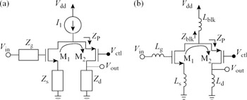
Figure 7.2: Folded cascode topologies: (a) wideband conventional, (b) narrowband modified
7.2.5 Gain control in the folded cascode structure
Linearity is becoming an important system design issue in today's wireless applications. Narrower allocated channel spacing drives the need for high linearity (i.e. IIP3), in addition to good noise and gain performance. Since high linearity usually trades off with high gain characteristics, gain controllability becomes a very desirable feature in modern LNA designs. This can enhance the IIP3 by decreasing the gain at high input-power levels. It also relaxes both the linearity requirements of other blocks in the receiver chain, and the dynamic ranges of the on-chip variable gain amplifiers (VGAs) at later stages.
There exist several types of variable gain amplifier (VGA) solutions in the literature (e.g. [18, 19]) as shown in Figure 7.3. They include (i) a switch-control type, which provides gain control by switching on/off active gain components, and (ii) the two-stage LNA–VGA type, which achieves gain control through the use of a VGA as a second stage. This extra gain-control functionality comes at the price of higher circuit complexity, which translates into an increase in power consumption and noise degradation.
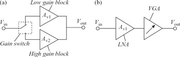
Figure 7.3: Conceptual views of variable gain amplifiers: (a) switch-control type, (b) two-stage LNA–VGA type
One of the main features of the topology in Figure 7.2b is that it readily provides gain control, with out any extra circuit complexity. Gain control can be simply achieved by varying the gate voltage (Vctl) of M2, which varies the impedance (ZP) looking into the source of the transistor, resulting in an overall variation of the gain of the LNA. We define the gain-tuning factor (Gtune) as representing the portion of the AC signal current, generated by the input transistor M1, which flows into the source of M2. It is given by
![]()
It is evident that Gtune can be adjusted by varying gm2, which is controlled by Vctl. Thus, the voltage gain (Atune) of the folded cascode structure in Figure 7.2b can be shown to be
![]()
where Av is the fixed voltage gain of a conventional cascode LNA [20], Zd2 is the impedance level at the drain of M2, and Qin is the quality factor of the input series RLC resonant tank.
Note that gain control is achieved without affecting the input noise and impedance matching, which are set independently by transistor M1. Hence, a low noise figure can be achieved while providing gain tuning. This is a considerable advantage when compared to other LNA architectures. For example, conventional cascode amplifiers (Figure 7.1b) do not have this flexibility in gain-control. The overall gain of the LNA is governed by transistor M1, while the cascode transistor M2 only acts as a current buffer. Gain control could only be achieved by altering the biasing current of M1, directly affecting the input noise and impedance matching, which is definitely not desirable.
To conclude, the modified folded cascode topology is a promising low-voltage structure, well-balanced in terms of stability and noise, with an inherent advantage of simple gain control compared to other architectures. In this work, all the LNA designs presented are based on this architecture, with a targeted operating frequency of 5 GHz and beyond.
7.2.6 Frequency control in the folded cascode structure
Frequency tunability can also be a desirable feature in LNA designs, as it can serve two main purposes: (i) to compensate for process variations and inaccuracies in inductor modelling, and (ii) to tune for a different receive band centre frequency. Frequency tuning was explored by adding a varactor at the resonant tank of the LNA as shown in Figure 7.4. There are a number of ways to implement a varactor. The one used in this prototype is an NMOS transistor over an Nwell, which makes use of the gate capacitance of the transistor [21, 22]. This structure has been reported to provide a wider tuning range and a better quality factor Q, in comparison to other PN or P+N junction-based varactors. This ensures a high Q for the resonant tank. For the prototypes with frequency tuning presented in this work, the varactors were designed to achieve a 10 per cent frequency tuning range.
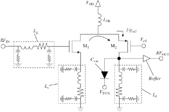
Figure 7.4: A single-ended fully tuneable (gain and frequency) low-voltage LNA
7.2.7 Design equations and optimisation
Designing CMOS RF circuits operating at frequencies greater than 1 GHz imposes many challenges and difficulties. Iterative circuit optimisation is often necessary. In this section, design equations, as well as a summary of inductor design guidelines and layout techniques, which have been adopted in this work, are presented.
7.2.7.1 Input impedance matching
Input matching is an important design issue, necessary to minimise signal reflection and noise. There is often a trade-off between noise and input impedance matching in LNA designs. This trade-off reflects on the choice of transistor sizing, which is mainly dependent on the designer's objectives and priorities. A common approach used is to first determine the transistor sizing which makes the circuit be approximately noise matched to the characteristic impedance of the system, typically 50 Ω, at the frequency of interest. Then, a minimal passive network is added to fine tune the input matching. For the LNAs in this chapter, a series-connected two-element matching network was used, as shown in Figure 7.5. It consists of gate and source inductors Lg and LS, respectively. The source degeneration inductor LS is used to match the real part of the input impedance to the characteristic impedance (Zs = 50 Ω), while the combination of source and gate inductors is used to cancel out the reactance due to the parasitic capacitance Cgs of the input transistor M1. The conditions for input impedance matching (Zin), and the expression for the resonant frequency ω0 are summarized as shown in Figure 7.5. Since a prime objective is noise minimisation, the matching network is designed to achieve the minimum overall noise figure, while still maintaining a reasonable input impedance matching, at the frequency of interest.
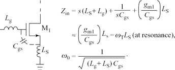
Figure 7.5: Conditions for input impedance matching
7.2.7.2 Integrated inductor design guidelines in CMOS
Proper modelling of integrated inductors at radio frequencies is one of the most challenging and crucial tasks in designing successful RFICs. Standard CMOS integrated inductors have inherently low quality factors (i.e. Q < 5) since they exhibit serious substrate and dielectric losses, which become dominant at GHz frequencies. This is mainly due to the high conductivity of the CMOS substrate. Substantial research efforts have been invested into this topic recently, attempting to improve the accuracy of inductor modelling and the quality factor of inductors in a CMOS technology. The main objective of this section is to provide guidelines and point out the trade-offs involved in inductor design in CMOS at RF.
Based on earlier work from the literature on inductor design (e.g. [23, 24]), there are a number of approaches to implement integrated inductors. Apart from the key geometrical parameters such as conductor width (W), number of turns (N), and inductor shape, the use of patterned ground shields and multilayer structures are other inductor design issues. Since the targeted operating frequencies in this work are at or above 5 GHz, the prime objective is to design inductors with high quality factors (i.e. Q > 5)atthosefrequencies, andtosimultaneouslymaximisetheirself-resonance frequencies, fRES, pushing them much higher than this range.
Although the use of a patterned ground shield will reduce eddie current losses at high frequency, and improve the quality factor, it can significantly reduce the fRES of an inductor due to the additional capacitive parasitics it introduces. Hence, in this work, a patterned ground shield is not inserted between the spiral inductor and the silicon substrate. Furthermore, the use of multilayer inductor structures connected in series in order to increase the self-inductance per unit area is not necessary, since the required inductances are in the order of 1–1.6 nH, which can be easily implemented with one simple planar structure. In order to achieve high Q through reducing the series resistance, the number of turns (N) should be minimised, while the conductor width (W ) should be made large. However, increasing W can have a negative effect on the self-resonance frequency, since wider metal traces translate into a larger parasitic capacitance to substrate. There exists an optimum value for W, which we found to be 20 μm. This result was obtained and verified by both simulation and experimental data [25]. Finally, to further reduce the series resistance of the inductor, two or three metal layers connected in parallel are used to emulate a thicker conductor.
7.2.7.3 RF layout techniques
Apart from proper modelling of integrated passives, layout is another important step in optimising high-frequency designs. Poor layout could result in large discrepancies between the actual and expected performance, or even result in a non-working circuit. The layout of a 5.8 GHz CMOS LNA is shown in Figure 7.6, to illustrate the RF layout techniques used in this work.
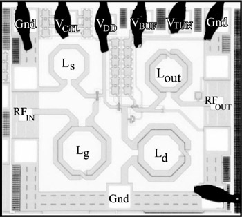
Figure 7.6: Micrograph of the 5.8 GHz CMOS LNA
Careful layout is observed in order to maximise performance. The layout is done in a uni-directional fashion, i.e. no signal returns close to its origin, to avoid coupling back to the input. The RF input and output ports are placed on opposite sides of the chip to improve port-to-port isolation. Since on-chip probing is used to measure the LNAs performance, standard ground-signal-ground (GSG) pad configurations are used at both the input and output RF ports. Furthermore, the signal pads (i.e. RF input and output) are implemented using the top metal layer only, in order to reduce RF signal loss through parasitic capacitances to the substrate. In order to minimise the effect of substrate noise on the system, a solid ground plane, constructed using a low resistivity metal-1 material, is placed between the signal pads (metal-6) and the substrate.
Since the operation of inductors involves magnetic fields, they can affect nearby signals and circuits, and cause interference. Therefore, inductors are placed far apart from each other, as well as from the main circuit components, with reasonable distances. Traces connected to all inductors are made wide enough to minimise series parasitic resistances and inductances, and thus avoid inductor Q degradation. Ideally, all interconnections should be as short as possible, to minimise the impact of parasitics. However, this is not always possible, especially due to the large geometrical structure of inductors when compared with components, such as transistors and resistors. When long interconnects become unavoidable in the layout, an in-house interconnect modelling routine [26] is used. The main purpose of this routine is to predict the additional parasitics introduced (e.g. inductances and resistances) and account for them in simulation, increasing accuracy during the design phase. Finally, line widths are set according to RF design guidelines, keeping DC traces thin and AC connections wide and as short as possible.
7.2.8 Measurement results – stand-alone LNAs
7.2.8.1 Gain and frequency controllable sub-1 V, 5.8 GHz CMOS LNA
The 5.8 GHz LNA was implemented in a standard 0.18 μm CMOS process. It features gain and frequency tuning capabilities. The experimental results were measured on wafer using GGB Industries Inc. picoprobes and a 20 GHz Agilent 8720ES vector network analyser. Standard short-open-load-through (SOLT) calibration procedures were performed before taking measurements. The measured forward transmission (S21) is shown in Figure 7.7. For a power consumption of 16 mW from a 1V supply, a power gain of 13.2 dB is achieved at 5.8 GHz, with a noise figure of 2.5 dB. The input and output reflection coefficients are less than −5 dB and −10 dB, respectively, as shown in Figure 7.8. The measured gain tuning of the LNA is shown in Figure 7.9. A gain control of over 12 dB is achieved, without affecting the optimum noise performance. The LNA exhibits a power gain greater than 7 dB at an extremely low voltage supply of 0.7 V (Figure 7.10), with a power consumption of 9.3 mW and a noise figure of 2.68 dB.
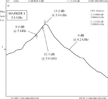
Figure 7.7: Measured power gain of the single-ended 5.8 GHz CMOS LNA with a 1 V supply
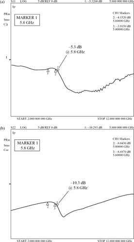
Figure 7.8: Measured (a) input and (b) output reflection coefficients of the 5.8 GHz CMOS LNA
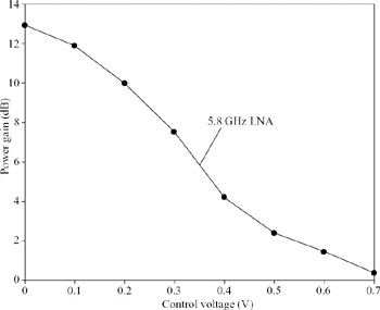
Figure 7.9: Gain tuning of the 5.8 GHz CMOS LNA
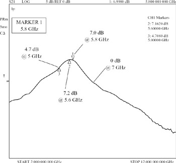
Figure 7.10: Measured power gain of the 5.8 GHz CMOS LNA with a power supply of 0.7 V
A plot of the frequency tunability of the LNA is presented in Figure 7.11. A continuous frequency tuning of 360 MHz, from 5.6 GHz to 5.96 GHz, is achieved using a simple varactor. This corresponds to a total tuning range of about 6 per cent, which is smaller than the expected range of 10 per cent that was predicted from simulation. An accumulation-type varactor was used. This structure has been reported to provide a wider tuning range (i.e. 30 per cent) and a better quality factor, in comparison to other PN or P+N junction-based varactors. A stand-alone varactor structure, which was fabricated on the same run as the LNA, was characterised. The measured capacitance tuning characteristics and quality factor of the varactor are shown in Figure 7.12. The measured capacitance variation is about 19 per cent, which is smaller than the expected 30 per cent. Furthermore, the measured quality factor of the varactor was found to be much lower than predicted, and is in the order of Q = 10. These differences are mainly attributed to the inaccurate initial varactor modelling, especially of the additive parasitic capacitances resulting after layout. The reduced tuning of the varactor limits the frequency tuning of the LNA. The system was designed to cover the complete 5–6 GHz frequency band, while the measured frequency tuning is limited to 5.6–5.96 GHz. The unexpected low quality factor of the varactor also has a direct impact on the resonant tank of the LNA. The estimated quality factor of the resonant tank (Qtank) of the LNA is about Q = 5.8. This was found to be lower than the Q factors of similar LNA implementations which did not use varactors for frequency tuning.
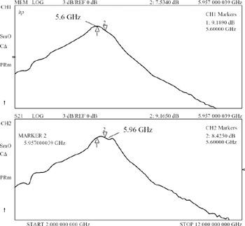
Figure 7.11: Frequency tuning of the 5.8 GHz CMOS LNA
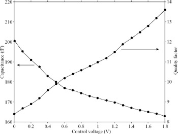
Figure 7.12: Capacitance tuning characteristics and quality factor of the varactors
7.2.8.2 Gain controllable sub-1 V, 8–9 GHz CMOS LNAs
Following the promising performance obtained from the 5.8 GHz LNA, two additional prototypes were fabricated, based on the same circuit topology, except for the absence of the tuning varactors. The microphotograph of the 9 GHz version is shown in Figure 7.13. The layout of the 8 GHz one is identical, except for the use of different inductor sizes.
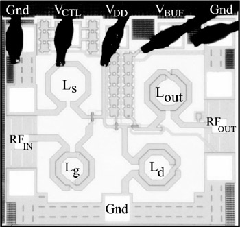
Figure 7.13: Micrograph of the 9 GHz CMOS LNA
The forward transmission (S21) plots of both designs are shown in Figure 7.14. For a power consumption of around 20 mW from a-1V supply, both prototypes achieved a power gain of 12–13.5 dB, with noise figures of 3.2–3.7 dB. Note that power gains of greater than 10 dB were achieved, over the frequency ranges of 6.7–8.6 GHz and 8.0–9.4 GHz, with the upper unity gain frequencies being at 10.8 GHz and 11.5 GHz, respectively. The input and output reflection coefficients of the two circuits are below −5dBand −13 dB, respectively. Both LNAs exhibit power gains greater than 5 dB at an extremely low voltage supply of 0.7 V (Figure 7.15), for power consumptions of around 10 mW. A gain control of over 10 dB is achieved without any increase in circuit complexity. The gain tuning characteristics of both designs are shown in Figure 7.16.
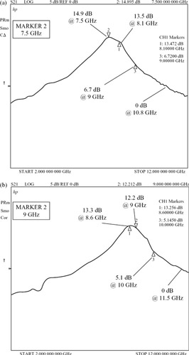
Figure 7.14: Measured power gain of the (a) 8 GHz and (b) 9 GHz CMOS LNAs
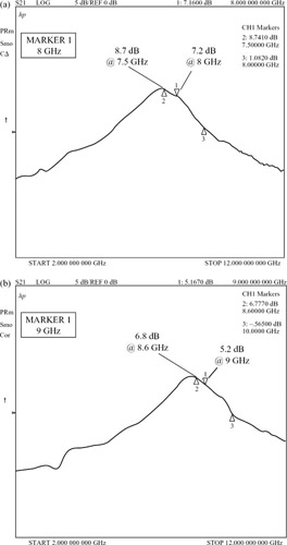
Figure 7.15: Measured power gain of the (a) 8 GHz and (b) 9 GHz CMOS LNAs with a power supply of 0.7 V
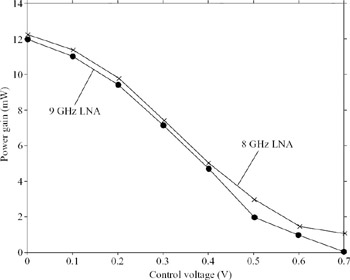
Figure 7.16: Gain tuning characteristics of the 8 and 9 GHz CMOS LNAs
It is interesting to note that, despite the higher operating frequency of the 9 GHz LNA, it has a relatively narrower bandwidth compared to the 8 GHz LNA. This is mainly due to the use of combined three metal layers (metal 4-5-6) for the inductors in the 9 GHz prototype, as opposed to the top two metal layers (metal 5-6) used in the 8 GHz circuit. This supports the fact that inductors with higher Q can be realised in CMOS by stacking more metal layers to emulate thicker conductors. The estimated quality factor of the resonant tanks (Qtank) of the 8 GHz and 9 GHz CMOS LNA are 6.2 and 6.6, respectively. Recall that the Qtank of the 5.8 GHz prototype was only 5.8 due to the use of varactors. The measured performances of all LNAs, under different biasing conditions, are summarised in Table 7.1.
| design Technology | 8 GHz LNA CMOS 0.18 μm | 9 GHz LNA CMOS 0.18 μm | 5.8 GHz LNA CMOS 0.18 μm | |||
|---|---|---|---|---|---|---|
| | ||||||
| Vdd | 1 V | 0.7 V | 1 V | 0.7 V | 1 V | 0.7 V |
| S21 | 13.5 dB | 7.1 dB | 12.2 dB | 5.2 dB | 13.2 dB | 7.0 dB |
| S11/S22 | −5.8/−13.9 dB | −10.9/−17 dB | −5.4/−11.9 dB | −9/−12.9 dB | −5.3/−10.3 dB | −7.1/−12.3 dB |
| Pdd | 22.4 mW | 10.7 mW | 19.6 mW | 9 mW | 16 mW | 9.3 mW |
| NF | 3.2 dB | 4.1 dB | 3.7 dB | 4.7 dB | 2.5 dB | 2.68 dB |
| Pin−1 dB | −13.2 dBm | −8.6 dBm | −8.9 dBm | −4.3 dBm | −14 dBm | −9 dBm |
| Gain tuning | 11.4 dB | 7.1 dB | 11.2 dB | 5.2 dB | 12.6 dB | 7.0 dB |
| Frequency tuning | − | − | − | − | 360 MHz 5.6−5.96 GHz | |
|
EAN: 2147483647
Pages: 100
- Chapter III Two Models of Online Patronage: Why Do Consumers Shop on the Internet?
- Chapter VII Objective and Perceived Complexity and Their Impacts on Internet Communication
- Chapter VIII Personalization Systems and Their Deployment as Web Site Interface Design Decisions
- Chapter IX Extrinsic Plus Intrinsic Human Factors Influencing the Web Usage
- Chapter XV Customer Trust in Online Commerce