7.4 A very low-voltage (0.8 V) 5 GHz CMOS receiver frontend
|
7.4 A very low-voltage (0.8 V) 5 GHz CMOS receiver frontend
Traditionally, RF receivers employed heterodyne architectures, using discrete filters for image rejection and channel selection. However, as the demand for higher integration increases, the direct conversion architecture has gained popularity, due to its simplicity and ease of integration. In this scheme, the RF signal is directly converted to baseband. Consequently, no image reject filter is required after the first amplification stage, and therefore the LNA does not need to drive off-chip high-quality filters.
Figure 7.27 shows the complete architecture of the receiver presented in this chapter, with the differential low-noise amplifier (LNA) connected to a set of I/Q mixers which are driven by a voltage-controlled oscillator (VCO) with quadrature outputs. The outputs of the I/Q mixers can subsequently be connected to another down-conversion stage to translate the IF signal to baseband, and thus implementing a Weaver image reject architecture (e.g. [37]). Another alternative is to directly process the IF signal, after being converted to single-ended by a transformer, using a highspeed ADC [38] followed by a digital signal processor, as suggested in Figure 7.27. The outputs of the mixers are capacitively coupled to the following stages in order to mitigate the effect of DC offset, resulting from LO leakage and signal feedthrough.
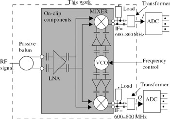
Figure 7.27: Receiver architecture
7.4.1 The differential LNA
Figure 7.28 shows a simplified schematic of the differential LNA used in the receiver, including all on-chip inductors. It is the differential version of the LNA discussed earlier in this chapter. In order to avoid added complexity and risk, the tuning capabilities discussed for the single-ended version were not explored in the receiver. Transistors M1 and M4 act as common-source amplifiers, and transistors M2 and M5 are used as common-gate current buffers with load inductors L7 and L9. Note that an added advantage of this structure is that, due to the higher voltage headroom, the transistors can be biased deeper into saturation, leading to an improved linearity. Also, this topology has shown improved reverse isolation.
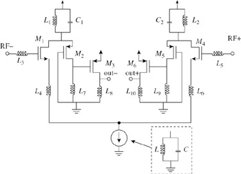
Figure 7.28: The differential LNA used in the receiver
The LC tanks, formed by inductors L1 and L2 and capacitors C1 and C2, behave as DC current sources. They provide the necessary DC bias current to the LNA, while presenting a high impedance to the RF signals. Also, a positive by-product of using an LC tank as such is to nullify the effect of the parasitic capacitances of the transistors, resulting in an improvement of the noise figure [14]. At resonance, the low quality factor of an on-chip inductor can cause the impedance of the LC tank to be small compared to the impedance seen at the sources of the PMOS transistors M2 and M5. As a result, the RF signal could be lost to the LC tank [15], thus the importance of ensuring the quality of the inductors used. In order to further maximise the voltage headroom, the biasing current source was also implemented as a resonating tank.
In order to achieve minimum noise, the widths of transistors M1 and M4 need to be set to their optimum values, Wopt. According to [39]
![]()
where ω is the operating frequency of the circuit in radian/sec, L is the minimum feature size of the fabrication process (0.18 μm in this work), Cox is the gate capacitance per unit area, and RS is the input resistance (50 Ω in this case). Inductors L3 and L4 are used for matching as explained earlier. Buffers formed using transistors M3 and M6 provide extra gain and increased isolation between the LNA and the mixer.
7.4.2 The mixer
The mixer (Figure 7.29), which is based on a double-balanced Gilbert active structure, down-converts the differential RF signal from 5.2 GHz to a 600–800 MHz intermediate frequency (IF). It consists of a pair of transconductors (M5–M6) and four transistors (M1–M4) which act as switches.
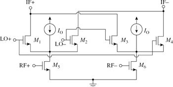
Figure 7.29: Schematic of the I/Q mixer
Although passive mixers generate less noise than active mixers, they require larger LO signals and provide no conversion gain, resulting in a severe noise figure deterioration. On the other hand, while active mixers can provide signal gain, they suffer from the noise induced by the transconductor and switching transistors. To mitigate the noise from the latter, which appears directly in the output signal path, extra current sources I0 are used as shown in Figure 7.29. This decreases the DC biasing currents of M1–M4, thus reducing their noise, while maintaining the high bias of transistors M5–M6 necessary to ensure a high RF gain [40].
To improve the mixer linearity, the differential input transconductor was built as a grounded-source differential pair, rather than a differential pair with constant current source biasing. A current source biasing would introduce third-order intermodulation products and lower the overall linearity of the mixer [41]. This also helps reducing the voltage headroom requirement.
Since the mixer is to operate from a 0.8 V supply, transistors with relatively large widths are used, in order to lower the threshold voltage required to bias the transistors in saturation. In addition, the gates of transistors M1–M4 are biased near threshold in order to minimise their switching time, thus reducing the output noise. The RF signals from the LNA are AC coupled to the inputs of the mixers, in order to allow the latter to set different DC biasing points. As for the loads at the IF outputs, they can either be resistive or reactive (e.g. an LC tank).
7.4.3 The quadrature voltage-controlled oscillator
The core structure of the VCO (Figure 7.30) consists of two pairs of cross-coupled transistors M1–M2 and M3–M4 with on-chip load inductors L1–L4. The two transistor pairs are coupled through transistors M5–M8 in order to provide quadrature outputs for both the I and Q paths [30]. Inductors L1–L4 resonate with the parasitic capacitors of the transistors to set the oscillation frequency, while the transistors provide the negative resistances necessary to overcome the inductor losses.
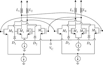
Figure 7.30: Schematic of the quadrature VCO
The output phase noise at an offset Δf from f0 can be approximated by the following relationship
![]()
where kT is the product of the Boltzmann constant with the absolute temperature, A is the noise factor safety margin necessary to ensure oscillation start-up, Vrms is the root mean square voltage at the oscillation nodes, and ![]() and Qtank are the tank characteristic impedance and quality factor, respectively. In order to ensure oscillation, the widths of the transistors in our design were slightly oversized to increase the safety margin A.
and Qtank are the tank characteristic impedance and quality factor, respectively. In order to ensure oscillation, the widths of the transistors in our design were slightly oversized to increase the safety margin A.
Varactors D1–D4, which are implemented as NMOS transistors over Nwells, are controlled with an external DC voltage source, Vc, in order to provide tuning capabilities. As a result, the tuning range of the VCO is around 5 per cent, from 4.4 GHz to 4.6 GHz. The size of the varactors is 100 μm. Larger varactors could be used to provide a wider tuning range, while adjusting the transistor sizes accordingly. Also, switched arrays of capacitors could be used for coarse tuning. Common-source buffers with inductive loads are used to increase isolation to the mixer, and to provide very desirable amplification for the VCO signals driving the mixers.
7.4.4 Measured characteristics of the receiver
The receiver was fabricated in a standard 0.18 μm CMOS technology from TSMC. Figure 7.31 shows a photomicrograph of the chip which occupies an area of 3.2mm 1.7 mm.
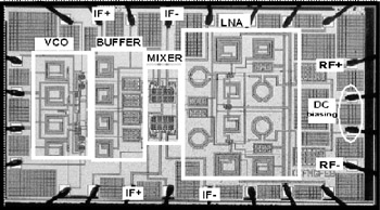
Figure 7.31: Receiver chip photomicrograph
A custom test fixture was built to characterise the fully packaged circuit (Figure 7.32). A passive ring hybrid balun structure on PCB is used at the input to convert the single-ended RF signal to a differential signal. A sliding capacitor, which slides along the two parallel transmission lines that connect the balun to the receiver chip, was used to match the input impedance of the receiver to 50 Ω. Figure 7.33 shows a plot of the resulting input reflection S11 of the receiver.
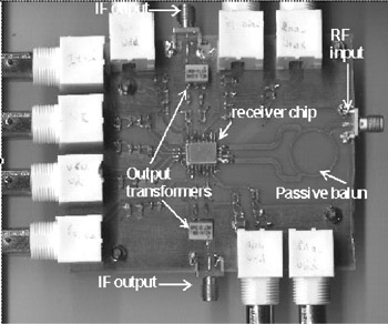
Figure 7.32: Printed circuit board test setup for the receiver
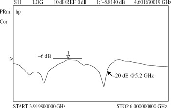
Figure 7.33: Input reflection S11 of the receiver
Resistive loads of 50 Ω are used at the mixer outputs. A surface mount transformer is then used to convert the output differential IF signal to single-ended for measurement via SMA connectors.
Figure 7.34 shows the measured output spectrum, without calibrating out the test set-up losses, for a two-tone test input at 5.2 GHz and 5.22 GHz. The fundamental signals appear at 680 MHz and 700 MHz, while the third-order intermodulation outputs, which are located at 660 MHz and 720 MHz, are −34 dBc below the fundamentals. The same set-up was used to obtain the overall conversion gain, the 1 dB compression point, and the IIP3 of the receiver. Figure 7.35 shows the third-order intercept plot, after calibrating out the losses of the test set-up (e.g. baluns, transformers, etc.). Table 7.3 summarises the measured receiver performance.
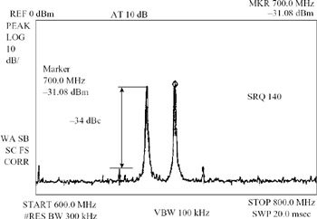
Figure 7.34: Receiver output spectrum for a two-tone test response, without calibrating out the test set-up losses
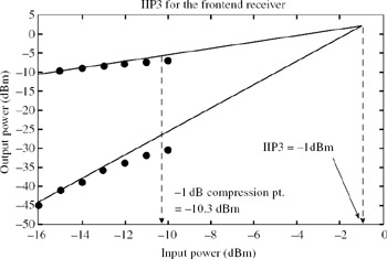
Figure 7.35: Receiver measured third-order intercept plot, after calibrating out the test set-up losses
| Overall conversion gain | 6 dB |
| (50 Ω system) | |
| VCO tuning range | 4.4–4.6 |
| GHz VCO phase noise | −100 dBc/Hz @ 500 kHz |
| Overall noise figure | 7 dB |
| Image rejection | 22 dB |
| Input S11 @ 5.2 GHz | −20 dB |
| IIP3 | −1 dBm |
| Input 1-dB compresssion | −10.3 dBm |
| Power dissipation @ 0.8 V | 56 mW |
| Die size (0.18 μm CMOS) | 5.44 mm2 |
|
EAN: 2147483647
Pages: 100