5.5 Performance
|
5.5 Performance
The reference transconductor was simulated to confirm its signal handling and the filter design was simulated to confirm its amplitude response, noise performance, signal handling, intermodulation distortion and rejection of power supply noise.
Under typical conditions, the single-ended transconductor (Figure 5.17) used transistors giving gmp = 19.94 μS and gmn = 19.99 μS and so G = 39.93 μS. It consumes 2.8 μA and has a quiescent input voltage of 0.756 V. When used in the differential transconductor and operated from an ideal 1.58 V supply rail, the simulated differential transconductance versus differential input voltage is as shown in Figure 5.19.
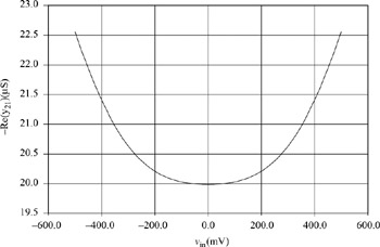
Figure 5.19: Simulated differential transconductance of 20 μS transconductor
The amplitude responses and group delay are shown in Figures 5.20 and 5.21 and indicate that they are very close to ideal. Figure 5.22 shows the passband of the filter with no feedthrough equalisation and this indicates the severity of high-frequency peaking due to non-reciprocal feedthrough capacitances and the effectiveness of the feedthrough equalisation technique.
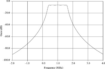
Figure 5.20: Simulated amplitude response
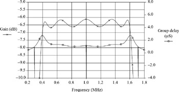
Figure 5.21: Simulated passband response and group delay
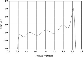
Figure 5.22: Simulated passband response without feedthrough equalisation
The 1 dB compression point occurred with a differential output swing of 1.3 V peak to peak (at 1 MHz), but the maximum differential voltage swing was restricted to 1 V peak to peak, corresponding to the maximum wanted Bluetooth signal of −20 dBm and required an input current swing of 40 μA peak to peak. Figure 5.23 shows an output NPSD in the passband of aproximately 90 nV/√![]() . The signal-to-noise ratio, found by comparing the power of the maximum signal with that of the noise integrated over 100 MHz bandwidth, was 68.2 dB.
. The signal-to-noise ratio, found by comparing the power of the maximum signal with that of the noise integrated over 100 MHz bandwidth, was 68.2 dB.
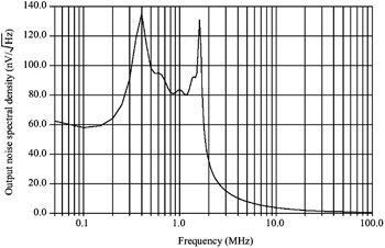
Figure 5.23: Simulated output noise spectral density
For the IM3 test, sinusoids at 4 MHz and 7 MHz with amplitudes 2 dB below the maximum signal were applied and the resulting simulated output spectrum is shown in Figure 5.24. The third-order product at 1 MHz was at a level of −86 dBV and this gives an IIP3 of 34.2 dBV.
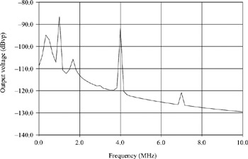
Figure 5.24: Simulated third-order intermodulation
For the supply noise intermodulation test, first Vdd and then Vss were modulated by a 1.5 MHz sinusoid while the input was driven with a 0.5 MHz sinusoid, each with amplitudes of 100 mV peak. These signals were both chosen to be in the filter's passband because this gave greatest intermodulation. The simulated output (nearly identical for either Vdd or Vss excitation) is shown in Figure 5.25 and indicates intermodulation products at 1 MHz and 2 MHz at 47.7 dB and 48.7 dB below the direct signal at 0.5 MHz. This attenuation of about 48 dB is maintained at lower input signal levels and is even greater for out-of-band supply noise.
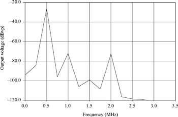
Figure 5.25: Simulated power supply-signal intermodulation
The total current drain for the whole Gm-C filter was 512 μA giving a power consumption of approximately 1 mW. The estimated chip area (including automatic tuning) is approximately 0.18 mm2. The results with nominal processing, at temperatures of −20 C, 27 C and 80 C, are summarised in Table 5.2 and indicate good stability of performance.
| Process | 2.5 V, 0.25 μm CMOS (C050FM) | ||
|---|---|---|---|
| | |||
| Filter shape | Chebyshev | ||
| Filter order | 5 + 5 | ||
| Filter ripple | 0.5 dB | ||
| Supply voltage (Vdd) | 2 V | ||
| | |||
| Temperature | −20 C | 27 C | 80 C |
| | |||
| Analogue supply(Vdda) | 1.568 V | 1.580 V | 1.607 V |
| Supply current (Idd) | 410 μA | 512 μA | 641 μA |
| Centre frequency (F0) | 1.036 MHz | 1.000 MHz | 0.952 MHz |
| Bandwidth (Fbw) | 1.241 MHz | 1.200 MHz | 1.143 MHz |
| Gain (A0) | −6.05 dB | −6.13 dB | −6.27 dB |
| Signal/noise (SNR) | 68.6 dB | 68.2 dB | 67.9 dB |
| IIP3 (4 MHz, 7 MHz) | 33.9 dBV | 34.2 dBV | 30.8 dBV |
| Supply intermodulation (0.5 MHz, 1.5 MHz) | −45.6dB | −47.7dB | −50.8dB |
| | |||
| Estimated chip area (filter) | ≈ 0.1mm2 | ||
| | |||
| Estimated chip area (tuning) | ≈ 0.08 mm2 | ||
With the transconductors deliberately skewed to emulate a 20 per cent mismatch between the transconductor's pMOS and nMOS transistors (the pMOS transistors were made 10 per cent wider and the nMOS transistors 10 per cent narrower), there were only minor changes to the typical performance as shown in Table 5.3. This justifies our claim that matching between the pMOS and nMOS transistor parameters is not critical.
| Transconductance ratio (kp/kn) | 1.0 | 1.2 |
|---|---|---|
| | ||
| Transconductor | ||
| Supply voltage (Vdd) | 2V | 2V |
| Supply voltage (Vdda) | 1.580 V | 1.586 V |
| Quiescent input voltage (Vin) | 0.756 V | 0.770 V |
| Transconductance (G) | 39.93 μS | 40.57 μS |
| Channel Filter | ||
| Centre frequency | 1.000 MHz | 1.014 MHz |
| Bandwidth | 1.200 MHz | 1.217 MHz |
| Passband gain | −6.13 dB | −6.27 dB |
| Signal/noise ratio | 68.2 dB | 68.2 dB |
| IIP3 (4 MHz, 7 MHz) | 34.2 dBV | 33.1 dBV |
| Supply intermodulation (0.5 MHz, 1.5 MHz) | −47.7dB | −47.7dB |
| Supply current (Idd) | 512 μA | 532 μA |
| Power dissipation | 1.024 mW | 1.064 mW |
Figure 5.26 shows the tuning loop (Figure 5.16) settling from start-up under typical conditions. It can be seen that the loop stabilises with the charge pump enable input, en, oscillating around 1 V and with its output, Qout, rising above Vdd to about 2.5 V with Vdda settling to its correct value of 1.58 V. Figure 5.27 shows that the simulated ripple on Vdda is less than 0.1 mV. With the switched capacitor varied by 40 per cent, the pole frequency of G/C stabilised to 1 per cent. Over the temperature range from −20 C to +80 C, the filter detuned by +3.6 per cent to −4.8 per cent. The output resistance of the Vdda regulator was about 80 Ω and the good rejection of Vdd and Vss disturbances reported above is due in large part to the attenuation of these disturbances by the regulating transistor by about 20 dB. The power consumption of the tuning loop was about 100 μW which is about 10 per cent of the filter's power consumption.
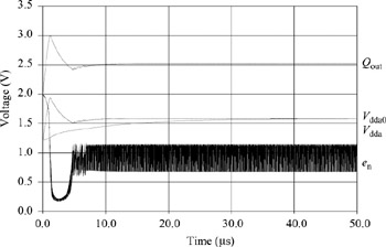
Figure 5.26: Simulated start-up behaviour of the tuning loop (see Figure 5.16)
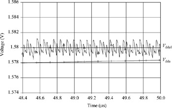
Figure 5.27: Simulated Vdda ripple of the tuning loop
|
EAN: 2147483647
Pages: 100