Nanowires
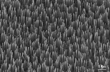
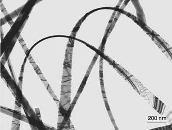
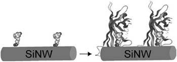
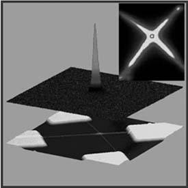
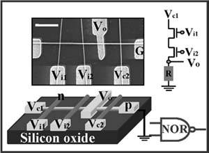
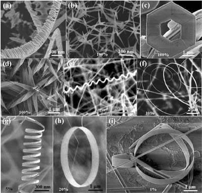
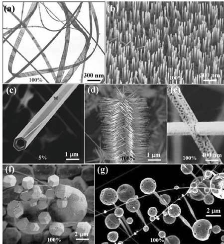
| Zhong Lin Wang Semiconductor nanowires (NWs) are wires only a few nanometers in size that do not occur naturally. They represent an important broad class of nanometer-scale wire structures, which can be rationally and predictably synthesized in single-crystal form with all their key parameters controlled during growth: chemical composition, diameter, length, doping, and so on. Semiconductor NWs thus represent one of best-defined and best-controlled classes of nanoscale building blocks, which correspondingly have enabled a wide range of devices and integration strategies (Figure 13-5). For example, semiconductor NWs have been assembled into nanometer-scale field effect transistors (FETs), p-n diodes, light-emitting diodes (LEDs), bipolar junction transistors, complementary inverters, complex logic gates, and even computational circuits that have been used to carry out basic digital calculations. It is possible to combine distinct NW building blocks in ways not possible in conventional electronics. Leveraging the knowledge base of chemical modifications of inorganic surfaces can produce semiconductor NW devices that achieve new functions and produce novel device concepts. Figure 13-5. Aligned semiconducting ZnO nanowire arrays. These wires are grown uniformly from a solid substrate, and their location and density can be defined by the deposited catalyst of gold. Semiconducting oxide nanobelts (NBs) are another unique group of quasi-one-dimensional nanomaterials with well-defined side surfaces, which have been systematically studied for a wide range of materials having distinct chemical compositions and crystallographic structures. Beltlike, nanobelts (also called nanoribbons) have been synthesized for semiconducting oxides of zinc (Figure 13-6), tin, indium, cadmium, and gallium by simply evaporating the desired commercial metal oxide powders at high temperatures. These oxide nanobelts are pure, structurally uniform, single-crystalline, and largely free of imperfections; they have a rectangularlike cross section with controllable dimension. Field effect transistors and ultrasensitive nanosize gas sensors, nanoresonators, and nanocantilevers have also been fabricated based on individual nanobelts. Thermal transport along the nanobelt has also been measured. Nanobelts, nanosprings, and nanorings that exhibit piezoelectric properties have been synthesized that could eventually be used to make nanoscale traducers, actuators, and sensors. Figure 13-6. Nanobelt of ZnO synthesized by a vapor-solid process. The nanobelt has a well-defined side surface, and it usually has a rectangular cross section. ApplicationsBiological Sensors Based on Individual NanowiresBecause many biological molecules, such as proteins and DNA, are charged under physiological conditions, it is also possible to detect the binding of these macromolecules to the surface of nanowires. Protein detection by SiNW nanosensors has been demonstrated for the well-characterized ligand-receptor binding of biotin-streptavidin (Figure 13-7) using biotin-modified NW surfaces. Figure 13-7. Detection of protein binding. The schematic illustrates a biotin-modified SiNW (left) and subsequent binding of streptavidin to the SiNW surface (right). The SiNW and streptavidin are drawn approximately to scale. Crossed p-n Junction Light-Emitting DiodesIn direct band gap semiconductors like InP, the p-n junction also forms the basis for critical optoelectronic devices, including LEDs and lasers (see Figure 13-8). To assess whether our crossed NW devices might behave similarly, the photoluminescence (PL) and electroluminescence (EL) from crossed NW p-n junctions can provide a means for controlling the color of the LEDs in a well-defined way. The ability to tune color with size in these nanoLEDs might be especially useful in future nanophotonic applications. Figure 13-8. Three-dimensional plot of light intensity of the electroluminescence from a crossed NW LED. Integrated Nanowire Logic DevicesThe controlled high-yield assembly of crossed NW p-n diodes and crossed-nanowire field effect transmitters with attractive device characteristics, such as high gain, enable the bottom-up approach to be used for assembly of more complex and functional electronic circuits such as logic gates. Logic gates are critical blocks of the hardware in current computing systems that produce a logic-1 and logic-0 output when the input logic requirements are satisfied. Diodes and transistors represent two basic device elements in logic gates. Transistors are more typically used in current computing systems because they can exhibit voltage gain. Diodes do not usually exhibit voltage gain, although they may also be desirable in some cases. For example, the architecture and constraints on the assembly of nanoelectronics might be simplified using diodes because they are two-terminal rather than three-terminal transistors. In addition, by combining the diodes and transistors in logic circuits, it is possible to achieve high voltage gain while simultaneously maintaining a simplified device architecture. The flexibility of these NW device elements for both diode- and FET-based logic has been demonstrated in the creation of AND, OR, NOR gates that have been used to implement simple basic computation (Figure 13-9). Figure 13-9. Logic NOR gate. Schematic of logic NOR gate constructed from a 1x3 crossed NW junction array. The insets show a sample scanning electron microscope image (bar is 1 m) and symbolic electronic circuit. Polar-Surface Dominated Novel NanostructuresFor applications in nanotechnology, ZnO has three key advantages. First, it is a semiconductor that has a direct wide-band gap and significant excitation-binding energy. It is an important functional oxide, exhibiting near-UV emission and transparent conductivity at room temperature and higher. It is also piezoelectric because of its noncentral symmetry. This is a key phenomenon in building electromechanical coupled sensors and transducers at nanoscale. The piezoelectric coefficient of a polar nanobelt is about three times that of bulk material, and this makes it a candidate for nanoscale electromechanical coupling devices. Finally, ZnO may be biosafe and biocompatible, so it can be used for biomedical applications without coating. With these three unique characteristics, ZnO could be one of the most important nanomaterials in future research and applications. The diversity of nanostructures presented here for ZnO should open many fields of research in nanotechnology. The synthesis of various nanostructures is based on a solid-state thermal sublimation process, in which a pile of source materials, typically the powder form of oxides, is placed at the center of a tube furnace. The source materials are sublimated by raising the temperature of the furnace; a redeposit ion of the vapor phase at a lower temperature zone produces novel nanostructures. By controlling the growth kinetics, the local growth temperature, and the chemical composition of the source materials, researchers have synthesized a wide range of polar-surface dominated nanostructures of ZnO under well-controlled conditions at high yield (Figure 13-10). Figure 13-10. A collection of polar-surface induced/dominated nanostructures of ZnO, synthesized under controlled conditions by thermal evaporation of solid powders unless specified otherwise: (a) nanocombs induced by asymmetric growth on the Zn-(0001) surface; (b) tetraleg structure due to catalytically active Zn-(0001) surfaces; (c) hexagonal disks or rings synthesized by solution-based chemical synthesis; (d) nanopropellers created by fast growth; (e) deformation-free nanohelixes as a result of block-by-block self-assembly; (f) spiral of a nanobelt with increased thickness along the length; (g) nanosprings; (h) single-crystal seamless nanoring formed by loop-by-loop coiling of a polar nanobelt; (i) a nanoarchitecture composed of a nanorod, nanobow, and nanoring. The percentage in each figure indicates the purity of the as-synthesized sample for the specific nanostructure in a specific local temperature region. Zinc oxide (ZnO) is a material that has key applications in catalysts, sensors, lasering, piezoelectric transducers, transparent conductors, and surface acoustic wave devices. This chapter focuses on the formation of various nanostructures of ZnO, showing their structures, growth mechanisms, and potential applications in optoelectronics, sensors, transducers, and biomedical science. For the nonpolar surfaces of ZnO, various forms of nanostructures have been synthesized for ZnO (Figure 13-11). These structures were realized by controlling growth kinetics. Figure 13-11. A collection of nonpolar-surface dominated nanostructures of ZnO, synthesized under controlled conditions by thermal evaporation of solid powders by controlling source materials, growth temperature, temperature gradient, and substrate. (a) Nanobelt; (b) aligned nanowire arrays; (c) nanotubes; (d) array of propellers; (e) mesoporous nanowires; (f) cages and shell structures; and (g) hierarchical shell and propeller structure. The percentage in each figure indicates the purity of the as-synthesized sample for the specific nanostructure in a specific local temperature region. |
EAN: 2147483647
Pages: 204