Section 6.1. I-UWB Radio Receivers
|
6.1. I-UWB Radio ReceiversI-UWB radio communicates with pulses of very short duration, typically on the order of a few nanoseconds, spreading the energy of the radio signal from near 0 to several GHz. Thus, I-UWB can accommodate a large number of simultaneous users [9, 10]. Regulatory considerations over such a broadband limit the radiated power and impose stringent pulse shaping requirements to comply with the FCC mask. Impulse radios, operating in the highly populated lower range of the frequency band below 3.1 GHz, must coexist with a variety of interfering signals, including self interference from multipaths and multiuser interference. Further, UWB signals must not interfere with narrowband radio systems operating in dedicated bands (legacy systems). To meet these requirements, spread spectrum techniques are often used. A simple means for spreading the spectrum of low duty cycle pulse trains is time hopping, with pulse position modulation for data modulation at the rate of many pulses per data bit. This signaling scheme is often described as time hopped pulse position modulation, or TH-UWB. Another technique of spreading the spectrum is direct sequence spread spectrum modulation, or DS-UWB. Recently, other schemes have been considered in order to obtain better performance in particular multiuser scenarios. In particular, time hopped phase shift keying (TH-PSK) and a novel technique based on pulse position modulation and optical orthogonal codes (OOCPPM) are considered in [11, 12]. In Section 6.1.1, we describe a generic system model that covers all the different kinds of spread spectrum multiaccess techniques proposed so far for I-UWB systems. Receivers for impulse I-UWB can be broadly categorized as threshold or leading edge detectors (LED), correlation detectors (CD), and RAKE receivers. Multi-user detectors (MUD) and hybrid RAKE/MUD-UWB receivers for robust narrowband interference suppression are becoming popular. We describe in depth LED, CD, and RAKE receivers for UWB systems in Sections 6.1.2, 6.1.3, and 6.1.4, respectively. MUD-UWB is discussed briefly in Section 6.1.5. Hybrid RAKE/MUD-UWB receivers are analyzed in sufficient depth in Section 6.1.6. Some of the other less popular methods of I-UWB signal reception and detection available in the literature are the sampling bridge circuit, integration and averaging, and template match detection [1315], which we briefly describe in Section 6.1.7. An alternative approach to UWB signal demodulation that has recently gained significant attention is the autocorrelation transmitted reference (TR-UWB) receiver [16]. We provide a detailed analysis of TR-UWB in Section 6.1.8. Synchronization and timing issues are examined in Section 6.1.9. A brief introduction to the concept of fully digital I-UWB receivers is described in Section 6.1.10. Section 6.1.11 describes Intel's proposal for impulse-based UWB communication. 6.1.1. System ModelIn this section, a general system model that captures all proposed spread spectrum multiaccess techniques for I-UWB is presented and the principle characteristics of the system are described [3]. The time axis is divided into symbol intervals of Ts seconds, each one further subdivided into smaller intervals called chips of duration Tc seconds. The signature sequence assigned to each user for multiple access purposes is a periodic signal with a period T seconds. For simplicity, we assume the baud duration T = Ns Ts and Ts = Nc Tc, where Ns and Nc may denote any positive integer values. The period T is longer than the symbol time Ts, whenever the multiaccess code spans more than a single symbol. The signal transmitted by user k can be represented as follows Equation 6.1 where Equation 6.2 and Let the UWB basic pulse waveform be denoted by w (t) with duration T w chosen such that Tw + max l (Tl) where Equation 6.4 The UWB channel model proposed by the IEEE 802.15.3a working group [1], is a modification of the Saleh-Valenzuela channel model [2]. This model takes into account the clustering phenomenon observed in several UWB channel measurements [3]. According to [2] the channel impulse response for user k can be modeled as Equation 6.5 where Assuming there are Nu active users, the received signal can then be written as Equation 6.6 where * denotes the convolution operation, Ak and Ab represent the attenuations due to path loss (which are a function of the transmitter receiver distance), n (t) is the white Gaussian noise process with two-sided power spectral density 6.1.2. Threshold/Leading Edge DetectionThreshold detectors, also known as leading edge detection (LED) receivers, were some of the earliest and probably the simplest of all I-UWB receivers [17, 18]. The LED receiver sets a threshold at the receiver, and any incoming pulse that crosses the threshold is detected and demodulated. The problem with the threshold reception technique is that noise spikes which happen to cross the threshold will also be erroneously detected as a data pulse (known as a "false alarm" or "false detection"). To mitigate the problem of false detections, the receiver must continuously monitor the input noise signal and adaptively set a threshold such that only a small percentage of false detections will occur, similar to the constant false alarm rate (CFAR) used in radar [19]. To operate properly, the LED receiver must use a device that is capable of responding to a very sharp change in received voltage in a very short time span. A tunnel diode, with its bistable operating point, would seem to be an ideal candidate for the leading edge detection receiver. However, its bias point varies with temperature, and a temperature compensation network must be designed into the receiver. The LED receiver is advantageous in that it is simple to implement and may be used for the case where only one pulse per data bit is transmitted. The LED receiver has some disadvantages. This receiver is susceptible to noise spikes and is incapable of taking advantage of multipath signals in the channel. Additionally, the receiver front-end, must, by necessity, have a very large bandwidth; any interfering signals (or intentional jammers) will either be sufficiently strong to cross the threshold and trigger numerous false detections or will cause the receiver to increase its threshold and reduce its range. We further study the threshold detector in detail next. The threshold receiver consists of a circuit fast enough to detect the presence of the I-UWB pulse, and some type of pulse stretcher or one-shot monostable circuit that outputs a pulse that is long enough for slower logic or analog circuits to process. Figure 6.2 is the basic block diagram of a threshold receiver. Note that the pulse stretcher can be viewed as a power gain because the energy in the output pulse is much greater than in the input pulse. Figure 6.2. Block Diagram of a Threshold Receiver. Threshold receivers tend to be simple circuits. An important characteristic of threshold receivers is that they are capable of detecting a single pulse. But, because they respond to a minimum amplitude, threshold receivers cannot take advantage of collecting energy from multipath components, and they are sensitive to noise and interference. The earliest threshold receivers employed tunnel diode bistable circuits. Figure 6.3 is a tunnel diode bistable circuit suitable for a threshold detector. A tunnel diode is connected to a broadband antenna, and the bias current through the diode is adjusted to point A in Figure 6.4. The voltage from the antenna is applied across the diode, and when the sum of the antenna voltage and the voltage at point A exceeds the peak voltage, VP, the diode is pushed over into the negative resistance region. The voltage across the diode rapidly rises to the stable bias point B. The diode must be reset at some point by interrupting the diode current or by forcing the diode voltage below VP. The external reset circuit can be conventional slow speed circuitry and integrated with the pulse stretcher. Figure 6.3. Tunnel Diode Peak Threshold Circuit Suitable for an I-UWB Receiver. Figure 6.4. I-V Characteristic of a Tunnel Diode Peak Threshold Circuit. A complete tunnel diode threshold detector circuit is shown in Figure 6.5 [17]. The diode current is set by R1. When the threshold is exceeded by a signal from the antenna, the voltage across D1 rapidly becomes more negative, and Q1 begins to conduct turning on D3 and D4. The result is that the current through R1 that normally biases the tunnel diode D1 is now shunted through Q1. This forms a regenerative loop because, as the current through the diode falls, the diode voltage drops below VP, cutting off Q1. The tunnel diode can now be retriggered. The conduction of Q1, D3, and D4 is relatively slow compared to the tunnel diode transition time. When Q1 conducts, it also drives the base of the avalanche transistor Q2 positive, starting the avalanche breakdown. R2 controls the avalanche point. When Q2 avalanches, it discharges the 680 pF capacitor. The output voltage is taken across the capacitor. Figure 6.5. Tunnnel Diode I-UWB Threshold Receiver.SOURCE: United States Patent 3,662,316, Short Base-Band Pulse Receiver, Kenneth W. Robbins, May 9,1972 [17]. 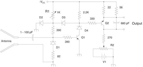 Avalanche transistors can be used for single hit threshold I-UWB receivers. Figure 6.6 is an avalanche transistor detector [18]. Q is biased for avalanche operation. The incoming pulse triggers the avalanche, and the energy stored in the transmission line begins to discharge into the load resistor, RL. The length of the output pulse is twice the propagation delay of the transmission line. The transmission line acts as the pulse stretcher. The pulse across RL triggers a one-shot monostable. During the one-shot time-out period, the input of the avalanche transistor is held low. This prevents triggering of the avalanche transistor while the transmission line recharges. If the time-out period is set just less than the expected interpulse period, the transistor cannot be retriggered on noise during the majority of the interpulse period. This simple time gating reduces the receiver's sensitivity to noise and interference. Figure 6.6. Avalanche Transistor I-UWB Detector. The main disadvantage of the threshold receiver is that any signal that exceeds the threshold will produce an output. This makes it sensitive to noise and interference. The threshold can be raised to reduce these effects at the cost of receiver sensitivity. An additional problem with the receivers in Figures 6.4 and 6.5 is that their threshold is sensitive to temperature variations. Temperature sensitivity can be reduced by applying feedback. The threshold receiver in Figure 6.7 employs a super regeneration technique [18] to reduce temperature sensitivity. The variable constant current source in Figure 6.7 charges capacitor C, resulting in a linear increase in the tunnel diode bias current. This change in bias is shown in Figure 6.8. The current through the diode increases until point 3 on the diode I-V curve in Figure 6.8 is reached. The tunnel diode then switches to its high voltage state. This transition triggers the first avalanche detector and the monostable pulse stretcher. Figure 6.7. Super Regenerative I-UWB Receiver.SOURCE: C. Bennett and G. F. Ross, "Time Domain Electromagnetics and Its Applications," Proc. of the IEEE [4] © IEEE 1978. Used by permission. 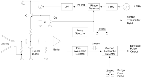 Figure 6.8. Bias Timing and Diode I-V Characteristics for the Receiver in Figure 6.7. The monostable output turns on Q2 in Figure 6.7. This discharges the capacitor, and the bias current through the emitter following Q1 drops to a low level. This resets the tunnel diode to its low voltage state. After the monostable times out, the capacitor charges again, producing a sawtooth current waveform through the diode, as shown in Figure 6.8. The pulse stretcher output is also fed to a phase detector. The phase error between the 10 kHz (100 sec) reference and the pulse stretcher output controls the capacitor charging current. If temperature causes the voltage at point 3 in Figure 6.8 to rise, it will take longer than 100 sec for the diode to switch. The resulting phase detector error voltage will increase the capacitor charging current, and the period of the sawtooth will be decreased. The result is that the most sensitive point on the diode's I-V curve is always reached at the same time. The receiver described in Figure 6.7 is used as part of the radar system. The transmitter is triggered 1 msec (99m sec after the reset) before the diode switches. The return signal finds the receiver in its most sensitive state just before transition. The output pulse from the first avalanche detector triggers the second avalanche detector only when the returned signal corresponds to the delay determined by the range gate. The feedback ensures that the receiver operates at the most sensitive point on the tunnel diode I-V characteristic independent of temperature, and the range gate activates the receiver only in the desired time window. This improves the receiver's stability and sensitivity at the same time, reducing its sensitivity to interference. The circuit in Figure 6.7 addresses the problem of temperature stability but it does not fully address the problem of the optimum threshold. The problem of a false output or a false alarm in threshold detectors is well known in radar systems [20]. The number of false alarms can rise dramatically with only a small change in the threshold. The sensitivity of threshold receivers can be increased by using the CFAR metric to adjust the threshold. The threshold of a CFAR receiver is constantly readjusted for a preset number of errors. Figure 6.9 is an example of a CFAR receiver [4]. The transmitter output only occurs on the odd cycles of the clock. On the even cycles, there is no transmitter output, so any output from the receiver is a spurious or false alarm output. Every time there is a spurious output, a "1" is clocked into the even cycle shift register, and when there is no output, a "0" is clocked in. The output of this shift register is summed and compared with the threshold set. This voltage can be adjusted to produce a given number of "1" hits in the shift register during any given time. The odd cycle shift register is also loaded with a "1" each time the threshold is exceeded. Because a pulse is transmitted during the odd cycles, it is more likely that the threshold will be exceeded by the signal. If the threshold is exceeded a preset number of times, a signal present output is generated. It should be noted that this CFAR receiver is no longer a single pulse detector. The effect of the shift register is to average either the noise, in the case of the even shift registers, or the signal in the odd shift registers. Figure 6.9. Constant False Alarm Rate (CFAR) Receiver.SOURCE: C. Bennett and G. F. Ross, "Time Domain Electromagnetics and Its Applications," Proc. of the IEEE [4]. © IEEE, 1978. Used by permission. 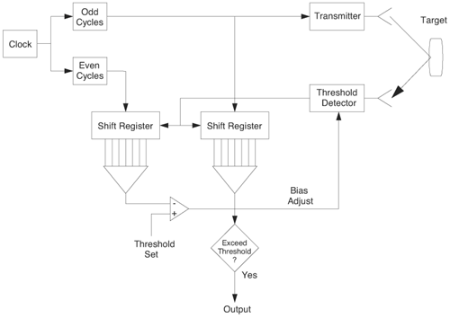 An analysis of threshold receiver performance is given by Harmuth [21]. Estimates of the probability of detection, PD, and the probability of false alarm, Pfa, are necessary in order to estimate threshold receiver performance. The noise and the signal pulse noise distributions are assumed to be Gaussian. The zero mean noise distribution is given by Equation 6.7 where Equation 6.8 and Equation 6.9 Because the received signal is the sum of the noise voltage and the signal voltage, the normalized signal plus noise voltage is given by Equation 6.10 Thus, the sum of the noise voltage and the signal voltage is also Gaussian distributed whose mean value is shifted by the signal. This results in a pdf for the signal, plus the superimposed noise given by Equation 6.11 The normalized pdfs for WN (x) and WN+S (x) are plotted in Figure 6.10. Suppose the threshold is given by F times sG or FsG. Any value of the noise pdf that exceeds the threshold is a false alarm, and any value of the signal plus noise pdf below the threshold is an error. By integrating the pdfs over the proper regions, the probability of detection, PD, and probability of false alarm, Pfa, can be computed as given by the following equations Equation 6.12 Equation 6.13 Figure 6.10. Threshold Detection in Gaussian Noise.SOURCE: H. F. Harmuth, "Radar Equation for Nonsinusodial Waves," IEEE Transactions on Electromagnetic Compatibility [21]. © IEEE, 1989. Used by permission. 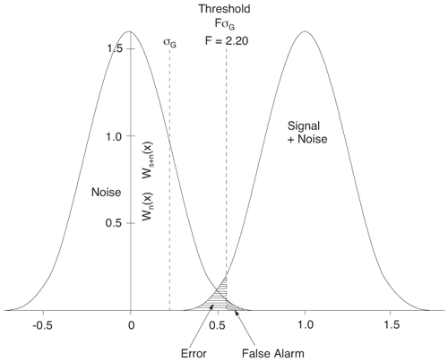 A 15 dB signal-to-noise ratio (SNR) is required for a 0.99 probability of detection with a 10-8 false alarm rate. Increasing the threshold decreases the false alarm rate but decreases the probability of detection for a given signal-to-noise ratio. 6.1.3. Correlation Detection (CD) ReceiversThe correlation detection (CD) receiver is also known as a matched filter receiver and has been used in narrowband communication systems for several decades. A block diagram of a simple correlation receiver is shown in Figure 6.11. The incoming pulse is multiplied by a template waveform. The output from the multiplier is a function of how well the template waveform generator matches the incoming waveform in time and shape. The correlation receiver is a matched filter system, and as such, it can provide the optimum detection SNR if the template waveform exactly matches the time and shape of the incoming waveform. Figure 6.11. Basic Correlation Receiver.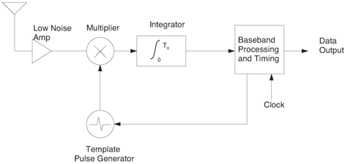 Next, we describe optimal matched filter and simple matched filter performance in multipath fading channels for A-PAM and PPM modulation schemes. We consider the case of a single-user system. For A-PAM modulation, (6.1) can be simplified and the transmitted signal can be written as Equation 6.14 where aj = ±1 are the data bits. We assume that the symbol or baud duration T is long enough to cancel any ISI effects. We also assume a simple L-tap multipath channel with impulse response given by Equation 6.15 where al and tI are the magnitude and delay of the lth path, respectively. Now the received signal may be written as Equation 6.16 Similarly for PPM, the transmitted signal can be written as Equation 6.17 where aj Optimal Matched Filter PerformanceIn this section, we derive an expression for the BER performance of the optimal matched filter. It is assumed that the filter template is exactly matched to the received signal. Such a receiver is studied in [22] for PPM modulation. By averaging over a large number of channel realizations, it is shown that the fading margin of this system is only 1.5 dB due to the ability of the UWB pulse to resolve multipaths. The optimal receiver provides a benchmark against which we can test performance of other suboptimal receivers. A-PAM ModulationAssume that we have perfect knowledge of the channel. The template used in the matched filter receiver is given by Equation 6.19 Hence, the decision statistic for the jth bit is given by Equation 6.20 Let Equation 6.21 Equation 6.22 Equation 6.23 where R (T) denotes the normalized autocorrelation of pulse w (t), and is defined as Equation 6.24 Thus, the BER is given by Equation 6.25 where Q (.) denotes the Gaussian probability integral, and the channel impulse response energy is assumed to be normalized to 1, Equation 6.26 upon averaging (6.25) over all possible channel realizations. PPM ModulationFor PPM modulation, the template is given by Equation 6.27 Now the decision statistic for the jth bit is given by Equation 6.28 Let u0 = E (g| aj = 0), u1 = E (g| aj =1) and s2 be the variance of z. We have Equation 6.29 Hence the BER is given by Equation 6.30 Simple Matched Filter PerformanceIn this section, we look into the simple matched filter receiver, which assumes that the pulse shape was not modified by the channel. The performance of such a receiver in an AWGN channel for A-PAM and PPM modulation is analyzed in [23]. A-PAM performance is identical to BPSK modulation in AWGN. PPM performance depends on the autocorrelation properties of the UWB pulse. An expression for the BER with PPM in a multipath channel is derived in [24]. A-PAM ModulationThe decision statistic for the jth bit at the output of this receiver is given by Equation 6.31 The decision rule is as follows Equation 6.32 For a specific channel realization, because the noise is a Gaussian random variable, r (t) also follows a Gaussian distribution, and z is therefore also a Gaussian random variable. We derive an expression for the BER by first finding the mean and the variance of z conditioned on a bit, and then applying the Q function for the decision statistics: The mean of z conditioned on aj = 1 is given by Equation 6.33 Similarly, the variance of z conditioned on aj = 1 is given by Equation 6.34 By symmetry, we have u-1 = -u1 and Equation 6.35 Note that the BER performance is limited by the factor PPM ModulationThe performance of a simple matched filter using PPM modulation was derived in [24]. The analysis is similar to the one discussed in the previous section. In this case the matched filter statistic is given by Equation 6.36 Thus, the BER can be computed as Equation 6.37 Where Equation 6.38 Equation 6.39 Equation 6.40 Notice that, in general, u0 and u1 are not equal. Performance of Matched Filter Based on PilotsWe now look at a receiver where the matched filter template is obtained by averaging N received pilot signals. Pilots are symbols known to the receiver and are primarily used in synchronization and channel estimation. This system can be thought of as a generalization of an autocorrelation or transmitted reference (TR) receiver discussed in Section 6.1.8. In a typical TR system, a pair of unmodulated and modulated signals is transmitted, and the former is employed to demodulate the latter. This receiver can capture the entire signal energy for slowly varying channels without requiring channel estimation. However, it suffers from the use of noisy received signals as a template for demodulation. In the subsequent sections we derive the BER performance of the pilot-based matched filters for A-PAM and PPM modulation schemes. A-PAM ModulationSuppose we use N pilots (modulated as ones) to estimate the correlator template. The estimated template can be written as Equation 6.41 or equivalently as Equation 6.42 The decision statistic for the jth bit is given by Equation 6.43 We first show the need for a bandpass filter at the output of the receiver. Assuming a '1' was transmitted, the decision statistic can be written as Equation 6.44 where Equation 6.45 The problematic term in (6.44) is Equation 6.46 We know that E [zn] = 0. The second moment of the zn is given by Equation 6.47 where Rn (t) and Rna (t) are the autocorrelation functions of n (t) and na (t) respectively. Moreover, we have Equation 6.48 Equation 6.49 Consequently, we have Equation 6.50 Equation (6.50) shows that the noise power at the output of the receiver is not limited. Thus, we need to band limit the signal first. The same conclusion applies to PPM systems. Assume that the signal is processed by a bandpass filter of bandwidth W and center frequency fc before passing through the "imperfect" matched filter. We assume that W is large enough such that ISI and interpulse interference are negligible. The new autocorrelation functions are given by Equation 6.51 Equation 6.52 Therefore Equation 6.53 The other two variance terms are Equation 6.54 Equation 6.55 where s' (t) is the filtered version of s (t). The total noise power is given by Equation 6.56 To obtain a BER in terms of Equation 6.57 Thus, the total noise power can be restated as Equation 6.58 where Equation 6.59 Equation 6.60 Now the BER can be calculated as Equation 6.61 Note that the noise term becomes negligible as Figure 6.12. Pilot-Based Matched Filter Performance for Varying Number of Pilots (T = 50ns).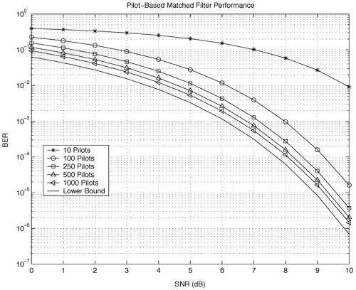 Figure 6.13. Pilot-Based Matched Filter Performance for Varying Integration Time (Pilots = 250).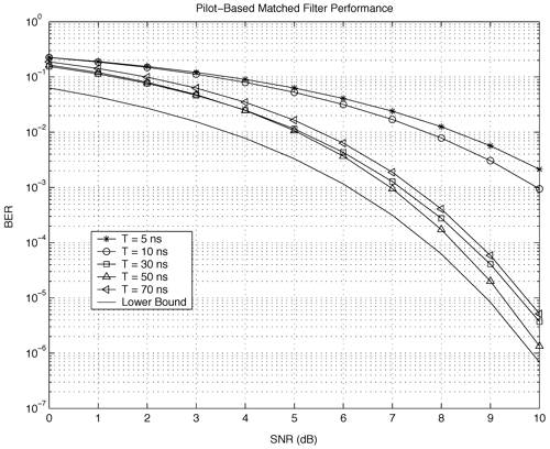 PPM ModulationA similar approach can be used to derive the BER expression for the pilot-based performance of PPM modulation. The decision statistic now is given by Equation 6.62 where s' (t), n' (t), and n'a (t) are the filtered versions of s (t), n (t), and na (t) respectively. The total noise power is contributed by three components as before, and is given by Equation 6.63 where Equation 6.64 Equation 6.65 Equation 6.66 Hence, the BER is given by Equation 6.67 Similar approaches can be adopted for the analysis of TH-PSK, OOC-PPM, and DS-PSK multiuser systems. BER performance curves are presented in Figures 6.14 and 6.15 [12]. Figure 6.14. Performance Comparison of Different I-UWB Systems in a 5 User System. (The BER of convolution encoded TH-PSK was obtained by simulation.)SOURCE: G. Durisi and S. Benedetto, "Performance Evaluation and Comparison of Different Modulation Schemes for UWB Multiaccess Systems," ICC 2003 [12]. © IEEE, 2003. Used by permission. 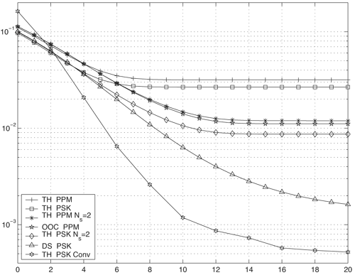 Figure 6.15. Performance Comparison of Different I-UWB Systems in a 14 User System. (The BER of convolution encoded TH-PSK was obtained by simulation.)SOURCE: G. Durisi and S. Benedetto, "Performance Evaluation and Comparison of Different Modulation Schemes for UWB Multiaccess Systems" ICC 2003 [12]. © IEEE, 2003. Used by permission. 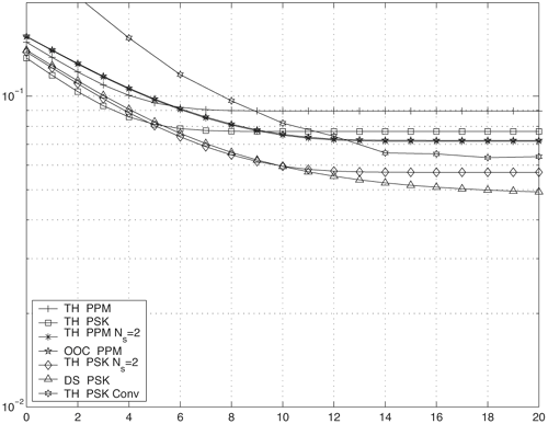 The CD receiver is advantageous in that the correlation operation can be done either in analog or digital circuits. The receiver can also take advantage of multipath signals by creating a bank of correlators, one for each multipath signal. The primary disadvantage of the CD receiver is imperfect correlations resulting from distorted input pulses. To correct this problem, an adaptive equalizer may be added or the CD receiver may be combined with the template match detection technique and perform a matched filter operation with a series of template waveforms, assuming the resulting increase in digital complexity is allowable. The LED receiver is sensitive to peak power while the CD receiver is sensitive to total received power. The SNR for the CD receiver is maximized by capturing all the energy in the incoming waveform. The SNR is degraded by a mismatch between the template waveform and the incoming waveform as well as timing errors. Figure 6.16 shows the effect of timing error on a correlation receiver. Figure 6.16. Correlator Receiver Output with Time Errors. The Temple Pulse Matches the Input Pulse. The Maximum Correlation Peak Occurs for Zero Time Offset. The Double Negative Peaks Are for 120 ps. Offset, and the Dotted Line Is the Output for 240 ps. Offset.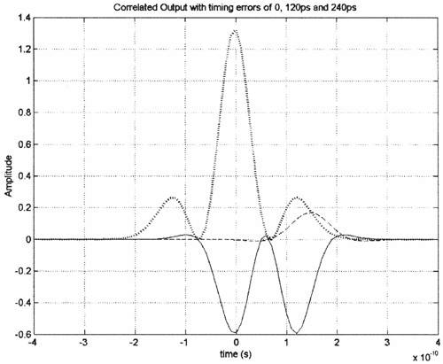 The basic building block of this receiver is the correlator. Therefore, the template that is correlated with the incoming signal is very important. In [25], the sinusoidal template for this receiver is compared with the ideal template. The optimal receiver matches the received waveform to the locally generated copy of the received signal. Assuming there is no intersymbol interference, and that a transmitted pulse only suffers from attenuation and delay (neglecting diffraction effects), the received signal would be a delayed and scaled version of the transmitted signal, which is a second derivative of a Gaussian pulse. This second order Gaussian pulse is difficult to generate using electronic circuits. Current system designs typically use a rectangular gate on the central peak of the receiver signal as a template. The sinusoidal template studied in [25] can simplify the UWB receiver structure compared to using the second order Gaussian derivative pulse template. A basic analog phase locked loop (APLL)-type UWB system is shown in Figure 6.17. Figure 6.17. Simplified UWB Correlation Receiver Using a Modified Analog PLL.SOURCE: S. Lee, "Design and Analysis of Ultra-Wide Bandwidth Impulse Radio Receiver," Ph.D. Dissertation [25]. © S. Lee, 2002. Used by permission. 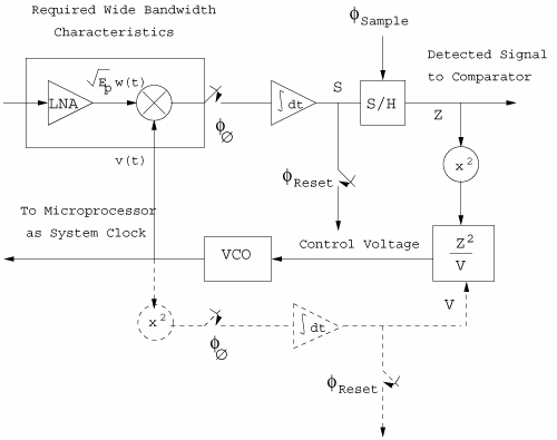 The switch between the multiplier and the integrator, and the sample and hold (S/H) block, controls the correlation time with respect to the hopping sequence. When the switch is on, the incoming signal correlates with the sinusoidal template. After the correlation, when the switch is off, the integrator works as the signal holder. The S/H block holds the correlated signal before the correlation output is reset. The VCO keeps generating template signals with the same pulse repetition rate that occurs when the switch is on. Therefore, the correlation output signal locks on the optimal template pulse repetition rate at the output of the VCO. Another advantage of this system is that the VCO provides the optimal clock signal to the microprocessor, which controls the time hopping sequence and integration time. The autocorrelation loop at the bottom half of Figure 6.17 ensures that the output of this system keeps the optimal SNR. The primary implementation advantage is that most of the hardware components used can be imported from the current technology, except for the low noise amplifier (LNA) and the mixer that is part of the correlator. Wide bandwidth LNA can be found on board-level designs that are used in basestations and radar systems, but it is hard to find them on chip-level designs. Design of the LNA and mixer for the LD receiver architecture is critical [25]. 6.1.4. RAKE ReceiversUWB systems development for high-speed indoor communications requires an analysis to establish which type of multiaccess and modulation format, and which receiver structure, offers the best compromise between complexity and robustness against multipath, multi-user and narrowband interference. As shown in [12], DS can better deal with multi-user interference than TH on AWGN channels. For a list of comprehensive literature on spread spectrum systems, see [26]. In this section, we present some of the receiver structures and design issues for DS-UWB systems. The RAKE receiver is used in any kind of spread spectrum communication system to accumulate the energy in the significant multipath components. A RAKE receiver is a bank of correlators. Each finger of the RAKE is synchronized to a multi-path component. The output of each finger is coherently combined using MRC (maximum ratio combining). Channel estimation is required in the combining scheme. Synchronization is critical in this form of receiver. RAKE receivers ideally reject out self-interference due to multipath effects, in addition to other forms of interference like multiaccess interference and adjacent channel interference, by using long, almost orthogonal spreading sequences like the PN or Gold sequence. RAKE receivers for CDMA systems are described in [26]. I-UWB RAKE receivers suffer from two major drawbacks. First, the energy capture is relatively low for a moderate number of fingers when Gaussian pulses are used. As we have seen, a typical NLOS channel can have up to approximately ~70 resolvable dominant specular components. Even if a RAKE receiver with so many fingers is possible, it would only be able to capture part of the signal energy. Second, each multipath undergoes a different channel, which causes distortion in the received pulse shape, and makes the use of a single LOS path signal as a suboptimal template [4]. Another issue is channel estimation. The energy-to-noise ratio available per path is given by Equation 6.68 where Pav is the average transmitted power, Tc is the coherence of the UWB channel, No is the one-sided power spectral density of the background receiver additive white Gaussian noise. It is seen that the energy-to-noise ratio per path is inversely related to the signal bandwidth; hence, it becomes increasingly difficult to estimate the channel coefficients at 7.26GHz. Channel estimation is critical in RAKE receivers for MRC, so degradation in performance is observed due to imperfect channel estimates. Synchronization (acquisition and tracking) is another major problem for pulses of subnanosecond duration. Also, the design of an all-digital RAKE receiver (similar to conventional RAKE for narrowband and wideband systems) is highly impractical. To summarize, UWB RAKE receivers suffer from two major drawbacks. First, the energy capture is relatively low for a moderate number of fingers when Gaussian pulses are used. It has been shown that a typical NLOS channel may have up to 70 resolvable dominant specular components. Even if a RAKE receiver with so many fingers is possible, it would only be able to capture part of the signal energy. Second, each multipath undergoes a different channel, which causes distortion in the received pulse shape and makes the use of a single LOS path signal as a suboptimal template [4]. Several papers investigate impulse radio systems using the AWGN channel or other simplified multipath channels where taps are spaced at an integer multiple of one pulse period [27, 28]. In general, several multipath components arrive during the duration of one pulse, which generates intrapulse interference. A fractionally spaced (FS) receiver can compensate for channel distortion due to intrapulse interference by sampling at least as fast as the Nyquist rate [29, 30]. An optimal maximum likelihood (ML) detector is far too complex to be implemented for a realistic system, so a suboptimal coherent RAKE receiver to reduce the complexity and still obtain diversity is presented in [31]. The coherent receiver estimates the delay, amplitude, and phase of the channel taps, but does not attempt to account for the correlation between received versions of the same signal. It is possible to reduce complexity even more by using noncoherent receivers that apply nonlinear operations on the received signal to eliminate the necessity of full channel estimation [31]. Such solutions incur additional performance losses. We briefly discuss coherent and partially/noncoherent RAKE receivers, and consider the problem of digital signaling over a frequency selective fading channel [24]. We consider a single-user system, and model the channel by a tapped delay line with statistically independent tap weights Equation 6.69 where the time-variant tap weights {ck (t)} are complex-valued stationary random processes. Assuming that the channel tap weights are known, the optimum demodulator consists of two filters matched to v1 (t) and v2 (t). The demodulator is sampled at the symbol rate, and the samples are passed to a decision circuit that selects the signal corresponding to the largest output. An equivalent optimum demodulator uses cross-correlation instead of matched filtering. In either case, the decision variables for coherent detection can be expressed as Equation 6.70 Figure 6.18[1] illustrates the operations involved in the computation of the decision variables. In effect, the tapped delay line demodulator attempts to collect the signal energy from all the received signal paths that fall within the span of the delay line and carry the same information.
Figure 6.18. Coherent RAKE Demodulator for Binary UWB Signals.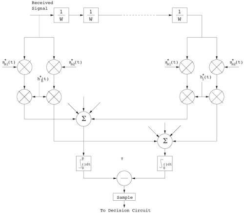 Channel estimation (estimating the tap weights) is crucial in RAKE demodulation and leads to complex receiver structures. If we choose not to estimate the channel, we may either use differential phase-shift keying (DPSK) signaling (partially coherent) or noncoherently detected orthogonal signaling. The RAKE demodulator structure for DPSK is shown in Figure 6.19. When the fading is rapid enough to preclude a good estimate of the channel tap weights or the cost of implementing the channel estimators is high, noncoherent RAKE with orthogonal signaling and square-law detection at the receiver can be used. The receiver structure of a square-law-based receiver is shown in Figure 6.20. The RAKE demodulator for orthogonal signaling is assumed to contain a signal component at each delay. If this is not the case, the performance will be degraded because some of the tap correlators will only contribute noise. The RAKE demodulator presented here can be generalized to multilevel signaling. In the following subsections, we further expand on the analysis of RAKE receivers for A-PAM and PPM modulation schemes with resolvable and nonresolvable paths and also analyze a realistic RAKE receiver. Figure 6.19. Partially Coherent RAKE Demodulator for DPSK-UWB Signals.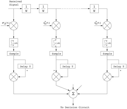 Figure 6.20. Noncoherent RAKE Demodulator for Square-Law Combining of Orthogonal Signals.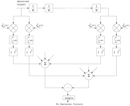 A-PAM ModulationResolvable PathsAssuming all paths are resolvable, that is, the minimum time between any two paths is larger than the pulse width, the template created by an F-finger RAKE receiver is given by Equation 6.71 where afi and tfi denote the amplitude and delay of the ith strongest resolvable paths respectively. Following the development leading to (6.19), the BER in this case is given by Equation 6.72 where the term Nonresolvable PathsLet us now assume that the two paths may be less than a pulse width apart. The autocorrelation function of the wave is now evident. We assume that the template constructed by the RAKE is still given by (6.71). Then the decision statistic is given by Equation 6.73 The mean and variance of the decision statistic can be readily shown as Equation 6.74 Equation 6.75 The BER is then given by Equation 6.76 where Figure 6.21. RAKE Performance for A-PAM Modulation and Perfect Channel Estimation. 500 ps Pulse Is Assumed.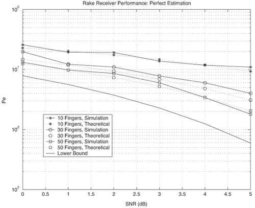 Figure 6.22. RAKE Performance for A-PAM Modulation and Imperfect Channel Estimation. 500 ps Pulse Is Assumed.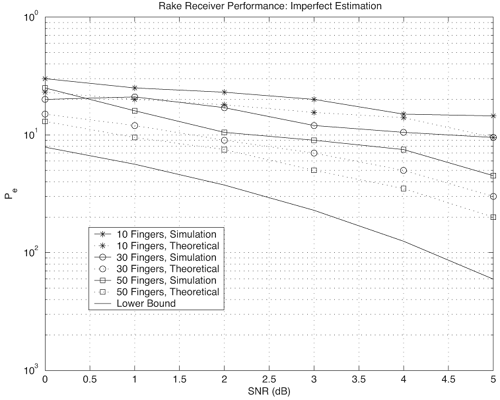 PPM ModulationResolvable PathsAssuming all paths are resolvable, the template created by an F-finger RAKE receiver for PPM modulation is given by Equation 6.77 Notice that all the fingers are shifted by d when a '1' is sent. Let us assume for now that d is greater than the pulse width. Because the mean and the variance of the decision statistic are given by Equation 6.78 Equation 6.79 we obtain an expression for the BER as Equation 6.80 Nonresolvable PathsWe now look at the more realistic case where the correlation among the paths is nonzero. The template reconstructed by the RAKE is still given by (6.77). The decision statistic is now given by Equation 6.81  The mean and the variance of the decision statistic are given by E[Z] = Ew Equation 6.82  Equation 6.83 The BER is then given by Equation 6.84  Realistic RAKE ReceiverIn this section, we derive the BER expression for a more realistic RAKE finger. The main assumption is that the RAKE receiver "knows" the location of the F strongest resolvable paths. However, the RAKE receiver has to estimate the MRC weights. Assume that the RAKE attempts to estimate the weight at a multipath with known delay tf. The correlator output is given by Equation 6.85 Equation 6.86 The term Equation 6.87 where nf is a zero mean Gaussian random variable with variance Equation 6.88 We can write z as Equation 6.89 where Equation 6.90 Equation 6.91 Equation 6.92 Equation 6.93 Because the variance of z is given by Equation 6.94 where Equation 6.95 Equation 6.96 Equation (6.94) can be written compactly as Equation 6.97 Figures 6.23 and 6.24 test the validity of this theoretical expression. When evaluating the theoretical expression, it is assumed that the F-finger RAKE receiver selects the F largest Figure 6.23. Testing Realistic RAKE Receiver Theoretical Expressions with 25 Fingers and 50 Pilots.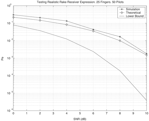 Figure 6.24. Testing Realistic RAKE Receiver Theoretical Expressions with 50 Fingers and 250 Pilots.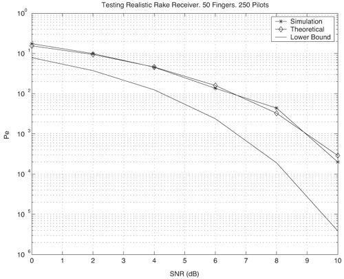 The performance of DS-UWB and TH-UWB for a single user link is compared for a data rate of 100 Mbps using the newly proposed realistic UWB channel model from IEEE P802.15 [32]. The IEEE UWB channel characteristic for four different scenarios is summarized in Table 6.1. The performance of suboptimal fractionally spaced (FS) coherent RAKE receivers with a pulse matched filter is evaluated for different channel estimation algorithms suitable for coherent detection. The FS-RAKE receiver is compared with pulse and symbol spaced RAKE receivers and an optimal maximum likelihood detector. The FS-RAKE receiver suffers 1 dB loss compared with the ML detector assuming perfect channel estimates, and the best evaluated channel estimation algorithm has a fractional loss compared with the perfect estimated channel. DS-UWB outperforms the TH-UWB by 2 dB when the transmitter-receiver separation is within 4 meters. Therefore, DS-UWB is more suitable for high-speed indoor links than TH-UWB systems. BER performance curves are shown in Figures 6.25 to 6.29. Figure 6.25. Different Detection Method with Perfect Channel Estimation for DS-UWB on CM1.SOURCE: B. Mielczarek, M.-Ol.Wessman, and A. Svensson, "Performance of Coherent UWB Rake Receivers with Channel Estimators," Proc. IEEE Vehicular Technology Conference [33]. © IEEE, 2003. Used by permission.
Figure 6.26. Different Channel Estimation Methods for DS-UWB on CM1 and CM2 Assuming 100 Pilot Symbols.SOURCE: B. Mielczarek, M. -Ol. Wessman, and A. Svensson, "Performance of Coherent UWB Rake Receivers with Channel Estimators, "Proc. IEEE Vehicular Technology Conference [33]. © IEEE, 2003. Used by permission. Figure 6.27. Different Channel Estimation Methods for TH-UWB on CM1 and CM2 Assuming 100 Pilot Symbols.SOURCE: B. Mielczarek, M. -Ol. Wessman, and A. Svensson, "Performance of Coherent UWB Rake Receivers with Channel Estimators," Proc. IEEE Vehicular Technology Conference [33]. © IEEE, 2003. Used by permission. Figure 6.28. Different RAKE Detectors for DS-UWB on CM1.SOURCE: B. Mielczarek, M. -Ol. Wessman, and A. Svensson, "Performance of Coherent UWB Rake Receivers with Channel Estimators," Proc. IEEE Vehicular Technology Conference [33]. © IEEE, 2003. Used by permission. Figure 6.29. TH-UWB and DS-UWB with Successive Channel Estimation Algorithm Using 100 Pilot Symbols.SOURCE: B. Mielczarek, M. -Ol. Wessman, and A. Svensson, "Performance of Coherent UWB Rake Receivers with Channel Estimators," Proc. IEEE Vehicular Technology Conference [33]. © IEEE, 2003. Used by permission. The RAKE receiver using maximum ratio combining (MRC) is optimal only when the disturbance to the desired signal is sourced by additive white Gaussian noise. Wireless personal area networks (WPANs), including those with a UWB physical layer, will be typically required to operate in proximity to other wireless networks. In the presence of narrowband interference, a UWB receiver with a conventional RAKE combiner will exhibit an error floor dependant on the signal-to-interference plus noise ratio (SINR). A more suitable diversity scheme to employ in this case is optimum combining (OC), whereby the received signals are weighted and combined to maximize the output SINR [34]. The minimum mean square error (MMSE) RAKE and eigen analysis-based eigen canceller (EC) are possible implementations of OC [35, 36]. The next sections discuss these receiver structures. The transmitter model assumed for the receivers in Sections 6.1.4 and 6.1.5 is shown in Figure 6.30. Figure 6.30. Narrowband Interference Model for DS-UWB.SOURCE: Q. Li and L. A. Rusch, "Muti-user Receivers for DS-CDMA UWB," IEEE Conference on Ultra Wideband Systems and Technologies [37]. © IEEE, 2003. Used by permission. 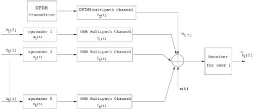 6.1.5. Multi-User Detection (MUD) UWB ReceiversThe effectiveness of MUD for an UWB pulse-based direct sequence spread spectrum system is described in [37]. It is shown in this chapter that adaptive minimum mean square error (MMSE) MUD receivers are able to gather the multipath energy and reject intersymbol and interchip interference for these channels to a much greater extent than conventional RAKE receivers. Adaptive MMSE is able to reject an IEEE 802.11a OFDM interferer even for SIR as high as 30 dB. The adaptive MMSE receiver exhibits only a 6 dB penalty in a 16 user case relative to the single user case. Practical RAKE receivers are incapable of effectively rejecting either strong narrowband interference or heavily loaded wideband interference. This chapter shows that even moderate levels of interference causes significant performance degradation of RAKE receivers. Figure 6.31 shows this MMSE MUD UWB receiver architecture. The BER performance plots to illustrate this are shown in Figure 6.32 and 6.33 [38]. Figure 6.31. MMSE MUD-UWB Receiver.SOURCE: Q. Li and L. A. Rusch, "Hybrid RAKE / Multiuser Receivers," Proc. Radio and Wireless Conference (RAWCON '03) [39]. © IEEE, 2003. Used by permission. Figure 6.32. TH and DS Performance in Presence of Strong Narrowband Interference. Six Asynchronous Users Are Active. BER Curves Are Depicted for Both RAKE and MMSE Receivers.SOURCE: G. Durisi, J. Romm, and S. Benedetto, "Performance of TH and DS UWB Multiaccess Systems in Presence of Multipath Channel and Narrowband interference," IWUWBS 2003 [38]. © IEEE, 2003. Used by permission. 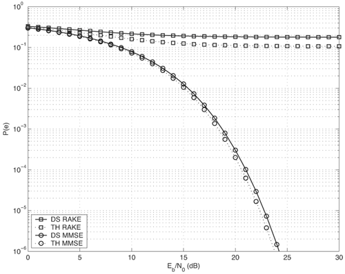 Figure 6.33. TH and DS Performance When Narrowband Interferers Are Not Active. BER Curves Are Depicted for Both RAKE and MMSE Receivers.SOURCE: G. Durisi, J. Romm, and S. Benedetto, "Performance of TH and DS UWB Multiaccess Systems in Presence of Multipath Channel and Narrowband interference," IWUWBS 2003 [38]. © IEEE, 2003. Used by permission. 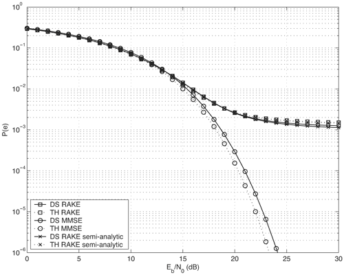 This receiver has high complexity, as the number of taps is equal to at least four times the length of the spreading code (for an observation window of two symbols and two samples per chip). The sampling rate of the analog to digital (A/D) converter is twice the chip rate, which for high bit rate systems leads to very high A/D sample rates. 6.1.6. Hybrid RAKE/MUD UWB ReceiversIn this section, we describe a hybrid RAKE MUD UWB receiver that is an enhancement of RAKE reception, replacing MRC combining with optimum combining based on MMSE or eigen analysis [hereafter referred to as the eigen canceller (EC)]. Minimum Mean Square Error (MMSE) MUD UWB RAKE ReceiverThee effectiveness of combining multiple arm RAKE reception with adaptive MMSE combining to combat both narrowband and wideband interference in a UWB pulse-based spread spectrum system is described in [39]. This receiver takes an N finger RAKE and replaces the MRC with an adaptive MMSE combiner. The proposed receiver offers robust suppression of narrowband interference for both a single user and a multi-user DS-UWB system as compared to the RAKE only receiver. The receiver provides much greater rejection of multiaccess interference (wideband interference), avoiding an error floor for moderate system load. RAKE reception alone exhibits an error floor at light system load. The proposed hybrid is considered as a reduced-complexity alternative to adaptive MMSE MUD-UWB. The new receiver gathers multipath energy and rejects intersymbol and interchip interference for the 2 8 GHz indoor channel to a much greater extent than simple RAKE receivers. It is also demonstrated that the adaptive combiner is able to reject the IEEE 802.11a OFDM interferer, even for signal-to-interference ratios (SIR) as severe as 30 dB. The adaptive combiner offers improved multiaccess interference rejection, with no visible error floor at 10-3 bit error rate. Simple RAKE receivers are incapable of effectively rejecting either the strong narrowband interference or the wideband interference. Figure 6.34 gives the block diagram for this receiver. The receiver essentially consists of a chip-matched filter (or suboptimally a bandpass filter) and an adaptive filter. The chip-matched filter suppresses noise and interference out of a signal band. The adaptive filter is an FIR filter that essentially acts as a correlator. The adaptive filter would perform minimum mean square error combining of the RAKE fingers using, for instance, the least mean squares (LMS) or recursive least squares (RLS) algorithm. The adaptation would be first to a known training sequence and later to data directed adaptation. While MRC is optimal in Rayleigh fading channels with additive white Gaussian noise, the adaptive MMSE filter is effective against narrowband and wideband interferers. The BER performance plots are presented in Figures 6.35 and 6.36 [39]. Figure 6.34. Hybrid RAKE/MMSE-MUD UWB Receiver.SOURCE: Q. Li and L. A. Rusch, "Hybrid RAKE / Multiuser Receivers," Proc. Radio and Wireless Conference (RAWCON '03) [39]. © IEEE, 2003. Used by permission.  Figure 6.35. BER Performance Comparison of RAKE MRC, MMSE MUD, and Hybrid RAKE/MMSE MUD-UWB in NLOS UWB Channels in the Presence of 5 UWB Interferers All with the Same Received Power.SOURCE: Q. Li and L. A. Rusch, "Hybrid RAKE / Multiuser Receivers," Proc. Radio and Wireless Conference (RAWCON '03) [39]. © IEEE, 2003. Used by permission. 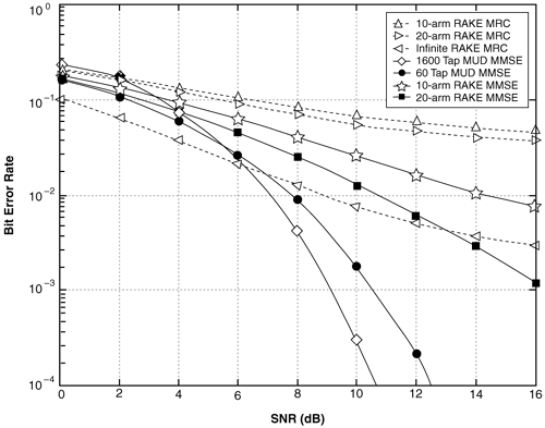 Figure 6.36. BER Performance Comparison of RAKE MRC, MMSE MUD, and Hybrid RAKE/MMSE MUD-UWB in NLOS UWB Channels in the Presence of 5 UWB Interferers All with the Same Received Power and One OFDM Interferer with SIR=-30 dB.SOURCE: Q. Li and L. A. Rusch, "Hybrid RAKE / Multiuser Receivers," Proc. Radio and Wireless Conference (RAWCON '03) [39]. © IEEE, 2003. Used by permission. 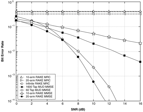 Eigen Canceller (EC) MUD-UWB RAKE ReceiverThe MMSE scheme is optimal in the sense that it achieves the maximum likelihood solution for Gaussian interference plus noise if the correlation of the received signal (aggregate of transmitted signals, interference, and noise) is known. When this correlation matrix has to be estimated, the MMSE solution is affected by measurement noise and is not optimal anymore. An eigen analysis-based OC scheme referred to as eigen canceller (EC) has been suggested for various applications, among them suppression of narrowband interference in direct sequence spread spectrum [40]. The EC exploits the inherent low rank property of the narrowband interference correlation matrix. It is designed as a weight vector orthogonal to the interference subspace. The interference subspace is defined as the signal space spanned by the eigen vectors associated with the dominant eigen values. For the method to be effective, the dominant eigen values need to be contributed mainly by the interference. This is the case for low SINR. The EC is motivated by the observation that the correlation matrix of the received signal consists of a limited number of large eigen values contributed by the narrowband interference and a large number of small and almost equal eigen values contributed by the desired signal and AWGN. A tap weight vector orthogonal to the interference eigen vectors effectively cancels the interference, leaving most of the data untouched. The EC is computed from relatively few, stable eigen vectors spanning the interference subspace. Thus even with a short data record it can obtain a high degree of interference cancellation. The next section compares MMSE and EC-based UWB RAKE receivers. MMSE Versus EC MUD UWB RAKE ReceiverWe briefly compare an MMSE versus EC MUD UWB RAKE over dispersive channels for TH-UWB for A-PAM and binary PPM modulation formats [41]. These ideas can be extended to DS-UWB. Consider a binary stream {dk} Equation 6.98 where Tf denotes the pulse repetition period. Polarity reversals can eliminate the spectral lines and reduce the peak-to-average power ratio. Two types of modulation, A-PAM and binary PPM, are considered. Hence, the following model is used for the received signal at time epoch k, namely, Equation 6.99 where the subscript k represents the bit index, Ts = TfNp is the symbol duration, tp is a PPM shift that ensures orthogonality between the two symbols of the modulation, I(t) denotes the narrowband interference and residual ISI, and the channel response h(t) is as given in (6.15). An optimum combining RAKE receiver is composed of L correlators followed by a linear combiner, as shown in Figure 6.37. The RAKE receiver samples the received signals at the symbol rate and correlates them with suitably delayed references given by Equation 6.100 Figure 6.37. Optimum Combining UWB RAKE Receiver for DS-UWB.SOURCE: H. Sheng, A.M. Haimovich, A.F. Molisch, and J. Zhang, "Optimum Combining For Time Hopping Impulse Radio UWB Rake Receivers," Proc. IEEE Conference on Ultra Wideband Systems and Technologies (UWBST '03) [41]. © IEEE, 2003. Used by permission. 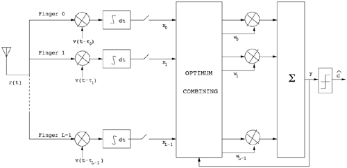 The received signal at the output of the correlator for the lth finger of the RAKE receiver can be written as Equation 6.101 while the received signal samples at the input to the optimum combiner (in a vector form) are given by Equation 6.102 where xk = [x0,k,. . ., xL1,k]T, h = [h0, . . ., hL1]T, Ik[I0,k,. . . ILl, k]T,and nk = [n 0,k. . ., nLl, k]T. A bit decision is made at the output of the combiner Concept of MMSE Receiver CombiningThe MMSE filter parameters are varied such that the mean squared error between the desired signal and the actual output is minimized. The minimum mean squared error (MMSE) criterion intends to find a weight vector that will minimize the mean squared error (MSE) between the combined signal and some desired (or reference) signal. The error signal can be defined as Equation 6.103 where ak is the reference signal. The weight vectors are estimated from a training sequence that is known to the receiver. The MSE is given by Equation 6.104 where Equation 6.105 is equal to the null vector. We have the optimum weight defined as wMMSE, and the following relation using (6.104) and (6.105) Equation 6.106 Equation (6.106) is the well-known Weiner-Hopf equation, and the solution for optimal weights known as the Weiner solution is given by Equation 6.107 In practice, the matrix Rxx is estimated from a block of training symbols. The maximum likelihood estimate is given by the sample covariance matrix Equation 6.108 where N is the block size. Because training is an overhead function that consumes resources, it is of interest to develop techniques that can work with short training sets. It is well-known that the number of vector samples required in estimating a L x L correlation matrix within 3 dB of its true value is 2L [42]. For a dispersive channel resulting in a large number of nonzero taps L, a large number of samples is required to train MMSE. Concept of EC Receiver CombiningIn this section, a reduced rank optimum combiner based on an eigen analysis approach that is more robust to errors caused by short training sets is presented [41]. By eigen decomposition, the covariance matrix is expressed as Equation 6.109 where the columns of Q1 and Qn consist of the interference eigen vectors and noise eigen vectors respectively. The matrices LI and Ln are diagonal, and contain the interference and noise eigen values respectively. For an interference with band-width considerably smaller than the signal bandwidth, the eigen analysis of the interference-plus-noise matrix reveals a few large eigen values and a large number of small eigen values. The eigen vectors associated with large eigen values span the interference subspace. Because the interference subspace is orthogonal to the noise subspace, a tap weight vector residing in the noise subspace will effectively cancel the interference, leaving most of the information data unaffected. The tap weight of the EC is designed to minimize the norm of the weight vector while maintaining linear and eigen vector constraints given by Equation 6.110 Using the method of Lagrange multipliers, we define the objective function Equation 6.111 The derivative of the objective function with respect to wH is given as Equation 6.112 We have the optimum weight defined as w EC and the following relation Equation 6.113 Using the null constraint in (6.110) and the result of (6.113) we have the following result Equation 6.114 Using (6.113) and (6.114) we have the optimum weights for the eigen canceller as Equation 6.115 Equation (6.115) shows that the weight vector of the EC is constructed from the stable eigen vectors of the largest eigen values of the received signal. It is unaffected by fluctuations in the noise eigen values. This leads to a high degree of interference cancellation. Figures 6.38 to 6.40 compare the performance of MMSE and EC-based receiver combining. Figure 6.38. BER Performance Comparison of MMSE and EC Combiner with Selected L= 40 Largest Fingers over the 802.15.3a LOS Channel in the Presence of 802.11a Interference.SOURCE: H. Sheng, A.M. Haimovich, A.F. Molisch, and J. Zhang, "Optimum Combining For Time Hopping Impulse Radio UWB Rake Receivers," Proc. IEEE Conference on Ultra Wideband Systems and Technologies (UWBST '03) [41]. © IEEE, 2003. Used by permission. 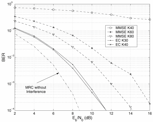 Figure 6.39. Comparison of the Output Power of the Interference Plus Noise as a Function of Training Data Size Between the MMSE and EC RAKE Receiver (L= 50 Taps are used).SOURCE: H. Sheng, A.M. Haimovich, A.F. Molisch, and J. Zhang, "Optimum Combining For Time Hopping Impulse Radio UWB Rake Receivers," Proc. IEEE Conference on Ultra Wideband Systems and Technologies (UWBST '03) [41]. © IEEE, 2003. Used by permission. 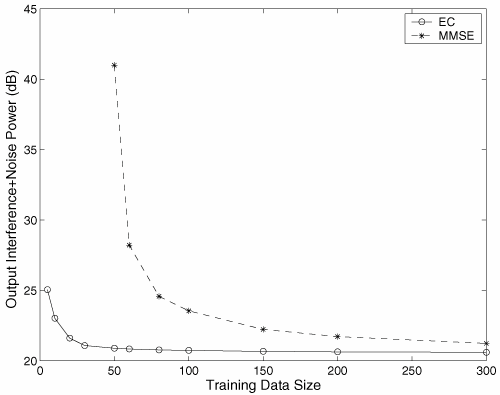 Figure 6.40. SINR Improvement as a Function of Input SINR in the Presence of 802.11a OFDM Interference over the 802.15.3a LOS Channel (L = 50 taps are used).SOURCE: H. Sheng, A.M. Haimovich, A.F. Molisch, and J. Zhang, "Optimum Combining For Time Hopping Impulse Radio UWB Rake Receivers," Proc. IEEE Conference on Ultra Wideband Systems and Technologies (UWBST '03) [41]. © IEEE, 2003. Used by permission. 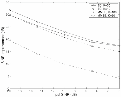 6.1.7. Other I-UWB ReceiversIn this section, we briefly describe three other less popular I-UWB receivers: template match detectors (TMD), the sampling bridge circuit (SBC), and integration and averaging (IA). In practice, researchers and companies use a combination of these and other techniques discussed in earlier sections. For example, O'Donnell has implemented a design based on a combination of the sampling bridge circuit and correlation detection that is capable of demodulating either pulse amplitude modulation (PAM) or PPM [43]. Time Domain Corporation has also implemented a similar design that demodulates PPM signals [44]. Immoreev uses a leading edge detection receiver with on-off keying [45]. Cellonics uses an integration and averaging receiver [46]. Template Match DetectionTMD receivers essentially take an input waveform and perform a cross-correlation operation with a bank of stored waveform templates to see which template generates a match. Abasicblock diagram of such a system is shown in Figure 6.41. Figure 6.41. Template Match Detection.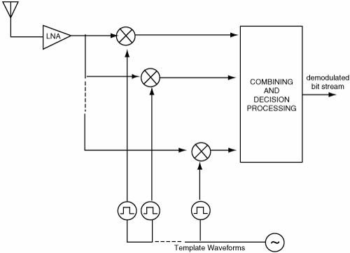 TMD reception would be useful if the receiver is expected to operate in a variety of environments that will impart a significant amount of pulse distortion, or environments that will try to jam the receiver by transmitting UWB-like pulses. The TMD technique, however, adds a significant amount of complexity to the receiver, thus limiting its practicality. Sampling Bridge CircuitThe SBC operates similar to a sampling oscilloscope by sampling the UWB signal at a very low rate (such as 200 Ksps) and combining multiple snapshots into a single received waveform. Typically, snapshots are sampled at random, interleaved intervals to ensure that the combined waveform is faithfully reproduced, a process that is illustrated in Figure 6.42. Figure 6.42. A Sampling Bridge Circuit Samples an Input UWB Pulse Train at Interleaved Intervals and then Combines the Various Snapshots into a Single Received Waveform. 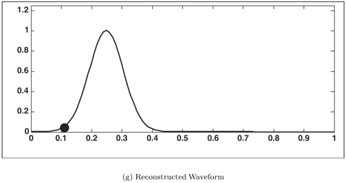 The SBC is most useful when a large number of pulses per data bit are being used by the UWB communication system, as it will automatically combine all of the transmitted pulses into a single received pulse. The SBC is an interesting approach in that by sampling a series of snapshots, the equivalent sampling rate may be very high, but the resulting data rate output is significantly reduced, thereby easing the requirements on the receiver hardware. The SBC also allows receivers to take advantage of multipath signals that may be present in the environment. A primary disadvantage of the SBC receiver is that it will only sample each input pulse a single time, with the individual samples combined together to produce a single pulse output. Thus, the SBC receiver does not fully realize the spreading gain that could be achieved if the total energy in each pulse were added together. Integration and AveragingThe Integrating and Averaging (IA) receiver is essentially a classical pulse compression receiver, where some number, N of high-rate pulses are combined into a single time dilated pulse. The IA receiver may be implemented similar to a sliding correlator channel sounder [29, 47]. For sliding correlator implementation, the time dilation is related to the slide factor, namely, Equation 6.116 where TfTX is the pulse repetition time for the transmitted pulses, TfTX is the pulse repetition time for the receiver pulse generator, k is the slide factor, TdOUT is the time duration of the pulse output from the sliding correlator, and TdIN is the time duration of the pulse input to the sliding correlator. For example, consider a system transmitting pulses 1 nanosecond pulse width at a rate of 10 MHz (TfTX = 10 ns ). The receiver correlates the pulses with a locally generated reference pulse clocked at a slightly faster rate (TfRX = 9.9 ns). Thus, the slide factor k = 100, and the output pulse has a duration of 0.1 microseconds. The net result of this sliding correlation operation is to reduce the requirements on the digital portion of the receiver because the output pulse may be sampled at a significantly lower rate as compared to the original input pulse. The primary disadvantage of the IA receiver is that a number of pulses must be transmitted per data bit as the receiver trades off a reduction in power and complexity for a lower data rate. 6.1.8. Autocorrelation Transmitted Reference (TR) UWB ReceiverThe fine time resolution of UWB signals results in the channel being extremely frequency selective. This results in a significant number of resolvable multipath components at the receiver. Thus, the need arises for a receiver structure tailored to achieve maximum energy capture. Research has mainly concentrated on the analysis of RAKE receivers. However, RAKE receivers applied to UWB systems suffer from two major drawbacks: First, the energy capture is relatively low for a moderate number of fingers when Gaussian pulses are used; second, each multipath undergoes a different channel, which causes distortion in the received pulse shape and makes the use of a single LOS path signal as a template suboptimal [16]. An alternative approach is the use of an autocorrelation receiver that correlates the received signal with a previously received signal [16, 48-50]. More precisely, a transmitted reference (TR) system is used, where a pair of unmodulated and modulated signals is transmitted, and the former is employed to demodulate the latter. This receiver can capture the entire signal energy for a slowly varying channel without requiring channel estimation. A potentially attractive feature of UWB autocorrelation receivers is their relative robustness to synchronization problems [49]. However, it suffers from the use of a noisy received signal as the template for demodulation. An analytical characterization of the performance of a UWB autocorrelation TR system can be found in [16]. Experimental results comparing the TR receiver with RAKE receiver structures can be found in [48]. It is shown that the TR receiver performs slightly better than a single finger RAKE receiver with coherent reception. The TR system described in [16] and [48] employs binary PPM. The transmitted signals consist of Np UWB pulses w (t) of duration Tw and energy Ew. The waveforms are comprised of Equation 6.117  where tw is the delay associated with PPM. Moreover, the authors take Then the received signal, assuming s0 (t) is transmitted, can be written as Equation 6.118  where g (t) = w (t) * h (t), Before demodulation, the autocorrelation receiver passes the signal through a bandpass filter of center frequency fc and bandwidth W. Note that W is an important design parameter in the system performance. In general, increasing W increases the energy capture at the expense of increasing the noise present in the demodulation stage. Because the UWB pulse occupies a wide frequency spectrum, the filter's bandwidth should be sufficiently wide so that no interpulse or intersymbol interference occurs. After filtering, the received signal is Equation 6.119 where To demodulate the ith data pulse, the receiver first multiplies the received signal during the (2i+1)th time frame with an appropriately delayed average of the Equation 6.120 The autocorrelator system is illustrated in Figure 6.43. The autocorrelator outputs corresponding to the two possible received signals are Equation 6.121 Figure 6.43. Autocorrelator System. The difference between the two outputs is calculated as Equation 6.122 where Equation 6.123 Equation 6.124  Equation 6.125 Equation 6.126  The term Equation 6.127 where Equation 6.128 Equation 6.129 Equation 6.130 Equation 6.131 For a specific channel realization, the following assumptions hold:
The reader is referred to [16] for a justification of these assumptions. The decision statistic is therefore Gaussian with mean given by Equation 6.132 where The probability of error is thus given by Equation 6.133 The terms z2, z3, and z4 in (6.133) are associated with the variances of Y2, Y3, and Y4 of (6.129), (6.130), and (6.131) respectively. For an extended discussion of these terms, the reader is referred to [16]. A similar BER expression for on-off keying (OOK) modulation is also included. Note that the third term in the denominator in (6.133) corresponds to the variance of Y4. This term becomes negligible at high SNR, while significantly degrading performance for low SNR or high TdW . In the following, we compare the autocorrelation receiver analyzed in [16] to a RAKE receiver. The analysis is performed using measured indoor channel data provided by Sholtz, et al [54]. Three different path selection schemes are investigated for the RAKE:
Although W (the width of the bandpass filter) is an important design parameter in the performance of the autocorrelation receiver, the filter bandwidth is not optimized in the experiment. The effect of the integration time Td on the autocorrelator's performance is studied. The BER performance is improved as Td is increased. The gains begin to diminish after a certain value of Td (20 ns for this experiment). When comparing the performance of the RAKE receiver and autocorrelation receiver, one must keep in mind that the autocorrelation receiver suffers a 3 dB penalty because half of the pulses are unmodulated. This 3 dB loss should be taken into account because although the RAKE receivers also require pilots for channel estimation, the data to pilot ratio is typically in the range of 101. In spite of the 3 dB penalty, simulation results show that the autocorrelation receiver (Td = 20 ns) performs slightly better than the first scheme RAKE receiver with one finger, better than the second scheme RAKE receiver with L = 4, and better than the third scheme RAKE receiver with L = 16. (Please compare Figures 6.44a and 6.44b [16].) Although the autocorrelation receiver captures a significant portion of the received energy, the performance is ultimately limited by the noise-on-noise term. Unless the effect of this term is limited, a RAKE receiver with multiple fingers will outperform the autocorrelation receiver. Figure 6.44. Performance Comparison of TR System and MRC RAKE Receiver. Note that at T = 40 ns, the TR System Performs Slightly Better than the MRC RAKE Receiver.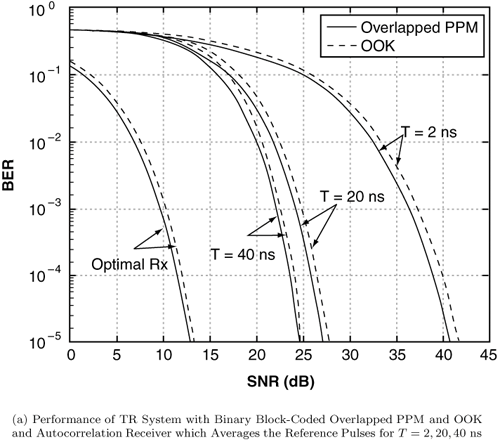 SOURCE: J. D. Choi and W. E. Stark, "Performance of ultra-wideband communications with suboptimal receivers in multipath channels," IEEE Journal on Selected Areas on Communications [16]. © IEEE, 2002. Used by permission. 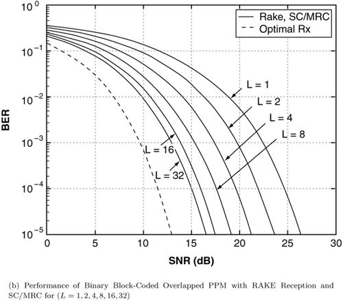 Results from [16] and [48] suggest that the autocorrelation system's performance is severely limited by the use of noisy unmodulated pulses as templates at the receiver. In fact, although the autocorrelator can potentially capture the total signal energy, the BER behavior suffers from the noise-on-noise term. Therefore, noise suppression techniques must be applied in order to obtain robust performance. Time hopping the unmodulated-modulated pair coupled with averaging at the receiver might hinder the effect of the noise term. Also, choosing an optimal value for the bandwidth of the receiver's bandpass filter plays a significant role in limiting the noise. Finally, more efficient signaling schemes can be investigated. In the design of I-UWB receivers it is important to take into consideration the effects of signal distortion due to diffraction by multiple frequency-dependent scatters [55]. Frequency-dependent dispersive effects are not a concern in narrowband systems because the characteristics of the receiver elements are essentially flat over small bandwidths. On the other hand, signal components at the low and high bounds of signal bandwidth will likely be affected by dispersion and loss. UWB generation affects receiver design because bandwidths depend on signal rise time instead of duration. The UWB signal may be viewed on a single pulse basis or as part of a string of pulses with specific intrapulse spacing. Each path of the multipath channel will have its own impulse response or frequency transfer characteristics. The frequency independence assumption is implied in the Turin model, which is widely adopted in tapped delay line models. This assumption is not true for I-UWB systems as in the case for radar target identification. Therefore, we should consider UWB signal distortion in the design of an optimum receiver that is coupled to the UWB channel propagation model. The physics behind the spatial-temporal resolution of scattering objects into multiple frequency-dependent scattering centers is described in [55]. UWB signal distortion due to multiple diffractions degrades the BER performance when a conventional correlation receiver is used. This is because the received UWB signal is a distorted version of the transmitted signal. Based on the matched filter principle, which is well-established in communications detection theory, optimum reception is obtained when the received signal is matched with a locally generated replica of the received signal. This is true for the narrowband case. Consequently, the correlation receiver is no longer optimum for UWB signal reception. A solution for this problem is to compensate for the diffraction by using a predistortion filter in the transmitter or by introducing a filter to restore the original shape of the received signal at the receiver. 6.1.9. Synchronization and Timing IssuesWith the exception of the LED receiver, all the previous receiver techniques require highly accurate synchronization with the transmitter, as well as accurate oscillators to maintain that timing. Particularly with PPM, proper synchronization and timing is essential to correctly demodulate the received signals because information is conveyed in the time position of the pulse. Figure 6.45 shows the cumulative effect of a 50 picoseconds offset in the timing of the transmitter and receiver pulse train. Note that after only a few pulses the two waveforms are no longer aligned. Figure 6.45. Effect of a 50 picosecond/pulse Cumulative Timing Error Between Transmit and Receive Pulse Trains.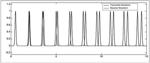 The timing offset will have a significant impact on the quality of the signal output by all the receiver techniques (with the exception of the LED receiver). Particularly, the TMD or CD receiver will see a dramatic drop in the SNR at the receiver output due to imperfect match or correlation with the receiver waveform. Additionally, if PPM is used and the cumulative timing offset becomes large enough, bit errors will occur. In addition to maintaining precise timing at the receiver, acquiring and synchronizing to the transmitted signal is essential for UWB communication systems. Currently, very little has been published in the area of synchronization, as many in the industry consider synchronization algorithms to be proprietary information. One known technique is used by Immoreev and involves transmitting a long stream of regularly spaced impulses only until the receiver acquires synchronization [5]. Whenever the receiver loses synchronization, the transmitter will return to transmitting a stream of synchronization impulses. In [6], the effects of timing jitter and tracking on the performance of binary and 4-ary UWB communications is analyzed, and it is reported that the performance of the Impulse Radio is very sensitive to timing jitter and tracking over a range of pulse interference levels. Another technique for acquisition and tracking is based on the sliding correlator principle. Bing, et al, has developed a "two-stage" technique that allows the receiver to acquire, capture, and track a UWB signal with a very simple hardware setup [57]. In their setup, the UWB transmitter produces pulses at a rate of 10 MHz. At the receiver, an identical copy of the transmitted pulse (the reference pulse) can be produced at rates of 10.01 MHz, 10.006 MHz, and 10.00 MHz. For coarse acquisition, the receiver first performs a sliding correlation operation with the reference pulse clocked at 10.01 MHz. After a correlation has been detected, the receiver switches to the 10.006 MHz clock signal in order to fine-tune the timing of the reference pulse. Finally, when the reference pulse is perfectly aligned with the received waveform, the receiver will switch to the 10.00 MHz clock signal, and begin demodulating data. The technique of Bing et al. is unique in that it does not require expensive hardware or signal processing techniques and can produce synchronization in a few milliseconds [57]. 6.1.10. Digital I-UWB ImplementationThe basic concept of a digital UWB receiver is to oversample the analog received signal (sample at equal to or greater than twice the Nyquist frequency) and then perform demodulation in the digital domain. Sampling the received signal may be accomplished using a Direct Sampling or a Time Interleaved Sampling approach. Direct Sampling involves sampling the received signal at a very high rate of, say, 1020 GHz. Thus, the overall waveform is essentially preserved, and demodulation in the digital domain may be performed. The major challenge in the Direct Sampling approach is implementing a very high-speed data bus to transfer the samples from the ADC to the digital hardware. For the best performance, the ADC and digital demodulation hardware should be implemented on a single IC, where the designer has very tight control over signal propagation delay and skew. While implementing such a high-speed data bus on a PCB is possible, taking care of clock synchronization, distribution, and signal propagation delay is a major design challenge. Implementing very high-speed ADCs may be difficult and expensive. Some parallel (or time interleaved) sampling approaches have been developed especially for UWB systems [58]. The idea behind Time Interleaved Sampling is to relax the requirements on the data bus while still sampling the received signal at a very high rate. Time Interleaved sampling is a quite common technique for high-speed oscilloscope design. Essentially, the received waveform is sampled by a number of ADCs operating in parallel, with each ADC clock slightly offset from the others, as shown in Figure 6.46. Thus, each ADC samples a slightly different point of the time domain waveform, and the effective sampling rate is the individual ADC sample rate multiplied by the total number of ADCs, as illustrated in Figures 6.46 and 6.47 with a set of 4 ADCs. Figure 6.46. Digital UWB Receiver with Time Interleaving ADC.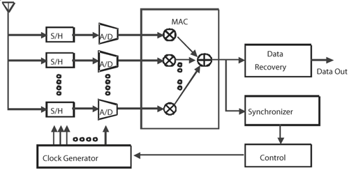 Figure 6.47. An Example Block Diagram of the Parallel Time Domain Sampling Technique Using 4 ADCs. An example of Time Interleaved Sampling is given in Figure 6.42 for a 5 ADC system. Typically, the signal is sampled at interleaved intervals by different ADCs to ensure that the combined waveform is faithfully reproduced. The time interval between the sampling of successive ADCs is given by t. That is, ADC #5 has a clock signal delayed by the same small interval t as compared to ADC #4, 2t as compared to ADC #3, 3t as compared to ADC #2, and so forth. The data bus that connects each ADC to the digital hardware is able to run at a much lower rate. Additionally, the digital hardware can re-create the received signal as if it had been sampled by a single, high-speed ADC. The trade-off is in complexity; instead of having a single high-speed data bus, we now have several lower-speed busses. Additionally, the use of multiple ADCs increases the power consumption and chip area required to implement the receiver. Finally, small imperfections in the clock signal delay, as well as clock jitter and ADC aperture delay, lead to slight variations in the exact point at which each ADC samplesresulting in distortion of the UWB signal. The Effective Sampling Rate of the Time Interleaved Sampling receiver may be represented mathematically by Equation 6.134 where 6.1.11. Example of IEEE Proposed Standards for PPM and DS-Based UWB ReceiversAn overview of the IEEE 802.15.3a preliminary standard that describes the MAC and PHY layers of a wireless personal area network (WPAN) can be found in Appendix 10.A. At the time of publication, the PHY layer was not fully determined. We briefly describe the IEEE proposed standard for the PHY layer by Intel Corporation [59] for PPM and DS-based UWB to get some insight into the implementation details, although PPM-based UWB is not part of the 802.15.3a standard. Intel's Proposal for PPM-Based UWBAn impulse-based system with 7.26 GHz bandwidth is considered. For polarity modulation, 1 bit/pulse, polarity and 2-PPM modulation, 2 bits/pulse and polarity, and 4-PPM modulation, 4 bits/pulse is proposed. The PPM transceiver has direct RF sampling and a 20 GHz 1-bit ADC with 1,280 parallel digital matched filters. Tunable notch filters are used at the transmitter for pulse shaping and to create spectral holes for coexistence or regulatory issues (to comply with the FCC mask) and also at the receiver for rejecting out narrowband interference. The PPM receiver processing involves a matched filter bank with infinite fingers RAKE performance that captures multipath energy and is assumed to be insensitive to pulse shape. The channel estimator provides 50 picoseconds resolution, which is a simple increment or decrement operation, and complex math is not required (1-bit samples). The pulse repetition frequency (PRF) is 185 MHz and can be varied. Convolutional code is used for FEC. The studies by Intel Labs have shown that PPM offers excellent performance in the worst multipath environments. The link budget assumes a 7 dB system noise figure and 123 Mbps at 10 meters range with a margin of 6.8 dB. The estimated power consumption is 200 mW for the complete receiver which is 5 mm2 in area. The channel estimator needs 175 K gates and is the dominant power consumer. Intel Labs have proposed reducing power consumption by MAC enhancements and also reducing the duty cycle to 10%. An all-digital scheme is also proposed because power will scale well according to Moore's law. Intel's Proposal for DS-UWBThe 7.26 GHz band is divided into three channels with center frequencies of 4 GHz, 7 GHz, and 9 GHz. The 7 GHz and 9 GHz channels are reserved for future use, perhaps for when the CMOS technology improves. This proposal avoids the 5 GHz WLAN bands worldwide. The emission bandwidth is restricted to 2 GHz. In the proposed DS-SS UWB system, the chip rate is 1 GHz and the modulation format is p/2-BPSK. Alternating 2 ns pulses on the in-phase and quadrature channels yields a constant envelope signal, thus easing CMOS implementation. The receiver processing uses a 4x oversampling rate (4 GHz). Four parallel despreaders are used for concurrent acquisition and channel estimation, which reduces the acquisition search time and also the RAKE multipath energy. The Viterbi decoder is not required at high SNR, thus reducing the power consumption using the software defined radio architecture. Individual or concatenated forward error correction (FEC) codes, convolution (r = 1/2, K = 7) and Reed Solomon codes (240, 224, 16), are used. The link budget assumes a 7 dB system noise figure, 4 GHz sampling frequency, and 115 Mbps at 10 meters range with margin of 7.7 dB. The link and the implementation margins are combined. The estimated power consumption is 150 mW for the complete receiver, which is 5-6 mm2 in area. The 115 Mbps operation is in a 0.18µ CMOS chip. | ||||||||||||||||||||||||||||||||||||||||
|
EAN: 2147483647
Pages: 110
- Step 1.1 Install OpenSSH to Replace the Remote Access Protocols with Encrypted Versions
- Step 2.1 Use the OpenSSH Tool Suite to Replace Clear-Text Programs
- Step 3.1 Use PuTTY as a Graphical Replacement for telnet and rlogin
- Step 3.4 Use PuTTYs Tools to Transfer Files from the Windows Command Line
- Step 6.3 X11 Forwarding


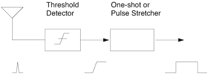
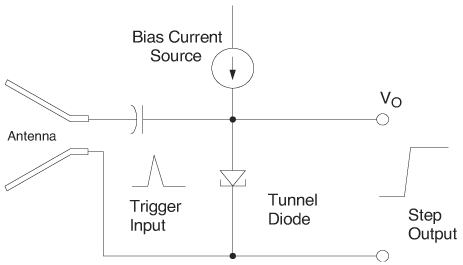
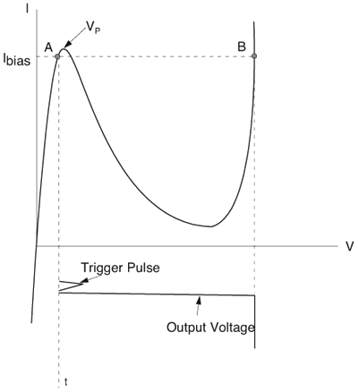
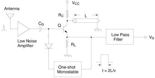


 {1,0} are the data bits, and


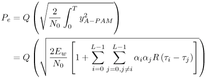


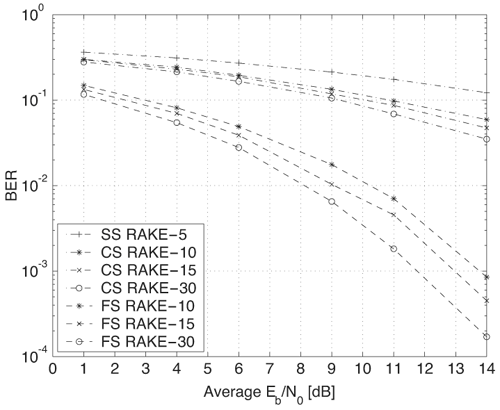
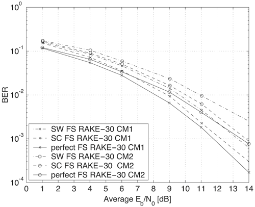
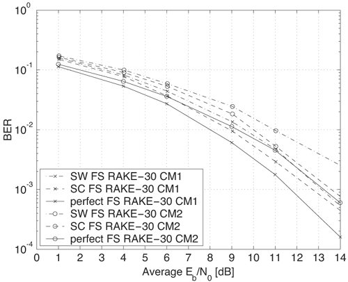
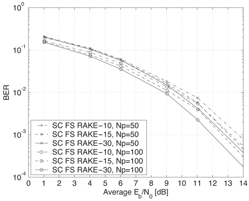
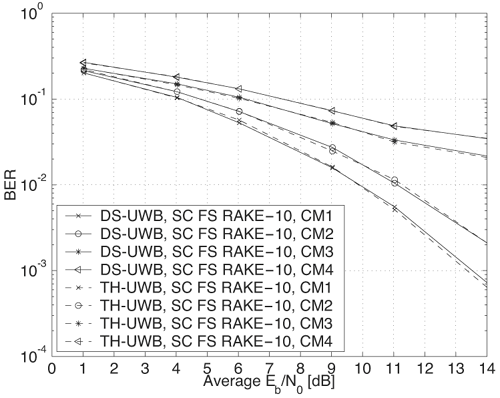


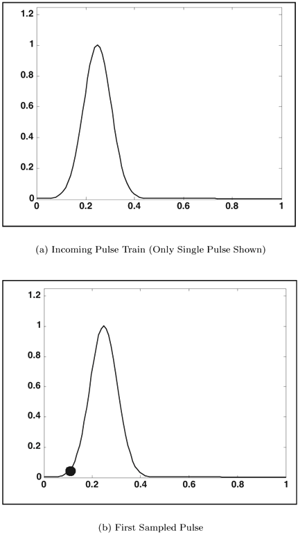
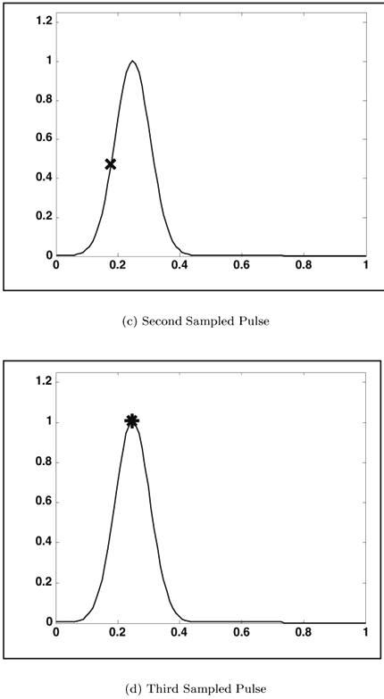
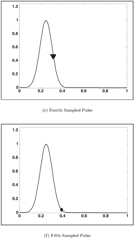

 '
'


