9.4 RF circuit syntheses
|
9.4 RF circuit syntheses
In the remainder of this chapter, two different types of amplifiers are optimised comparing the conventional and new adaptive simulated annealing with tunnelling algorithms: a class-E switching CMOS RF power amplifier and a CMOS RF wide-band distributed amplifier. Basic operation of the two amplifiers is explained before the circuits are synthesised using the parasitic-aware paradigm.
9.4.1 Class-E power amplifier
The class-E power amplifier, invented by Sokal in 1975, uses a transistor as a switch [9, 10]. If the switch is ideal, the voltage drop across its terminals is zero when it is on. On the other hand, when the switch is off, the current through it is zero. Hence, the power dissipated in the switch is zero since it is just the product of the voltage and current, one of which is always zero. However, if the switch is not ideal, there exist overlap times between the non-zero current and non-zero voltage waveforms which create power losses that reduce the power efficiency. The basic class-E concept is to use time delays implemented using capacitors and inductors to minimise the overlap times between the current and voltage waveforms in order to regain high efficiency. Figure 9.19 shows the basic structure of a class-E power amplifier and the associated waveforms. Since it uses a transistor as a switch, it is a non-linear power amplifier and is best suited for non-linear digital modulation schemes such as GMSK, MSK, etc.
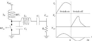
Figure 9.19: Basic circuit topology of a class-E power amplifier and its associated waveforms
Figure 9.20 shows a multistage power amplifier block diagram with typical gain and drain efficiency (η) distributions. To obtain high power gain, a three-stage PA is used. Figure 9.20a shows an example achieving 30 dB gain with 50 per cent drain efficiency. The drain efficiency of the third stage is most important because of its large output power. Hence, as shown in Figure 9.20b, the last two stages are class-E for high drain efficiency while the first stage is class-AB for high gain.
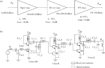
Figure 9.20: Three-stage CMOS power amplifier (class-AB, class-E, class-E) showing gain and drain efficiency (η) distribution
The first two stages use spiral inductors while the third stage and all choke inductors use bond wires. High quality bond wires must be used in the third stage because its output power is large.
To achieve one watt of output power
![]()
![]()
The resistance seen looking into the matching network connected to the 50 Ω antenna needs to be about 5 Ω. Unfortunately, the parasitic series resistance of the spiral inductor is greater than 5 Ω, and since it forms a voltage divider with the output load, it is impossible to deliver 1 W output power to the antenna. Hence, the bond wire inductor with its extremely small series resistance is used in the third stage.
To reduce the voltage stresses on the MOSFETs, cascodes are used in all three stages. HSPICE simulations were performed using the TSMC 0.35 μm CMOS parameters. The most important cost function components of a switched power amplifier are output power and drain efficiency.
Optimisation of this particular RF power amplifier involves 22 design parameters; the cost function is aimed at achieving at least 55 per cent drain efficiency with at least 1.2 W output power.
The specific cost function of the power amplifier examined here is
![]()
where weight_Pout and weight_EFF are weight parameters of Pout and EFF (efficiency).
According to equation (9.12), the output power needs to be exactly 1.2 watt, and the drain efficiency needs to be greater than 55 per cent to minimise the cost function. In this simulation, weight_Pout and weight_EFF are set to 50.
9.4.2 Class-E power amplifier optimisation results
Since the value of Temp is critical for both simulated annealing algorithms in comparing the tunnelling and conventional hill climbing processes, the new adaptive Temp coefficient algorithm is used to set Temp equally in both, for comparison purposes. The maximum iteration count is set to 20,000 in both cases.
Figure 9.21 compares the two approaches for a total of 12 synthesis runs. With tunnelling, the optimum is always found within 8,000 iterations; 41 per cent of the simulations find the optimum within 4,000 iterations. In contrast, for conventional simulated annealing without tunnelling, 25 per cent of the simulation runs do not find the optimum solution within 20,000 iterations; moreover, only 20 per cent of the runs find the optimum within 4,000 iterations. Clearly, the tunnelling process is superior to conventional hill climbing in escaping from local minima and accelerating the optimisation.
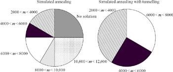
Figure 9.21: The number of iterations required to find the optimum solution for simulated annealing without and with tunnelling (12 synthesis runs) with power amplifier
Figure 9.22 plots the cost function trajectories versus the number of iterations for both the conventional and adaptive simulations. As shown, when the cost is low, many simulations are wasted in conventional annealing compared to the advanced local optimisation algorithm.
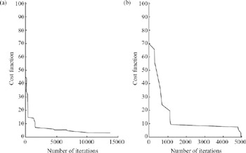
Figure 9.22: Cost function trajectory versus the number of iterations in (a) conventional and (b) adaptive simulated annealing with tunnelling. Note the different x-axis scales
The tunnelling process is superior to hill climbing in escaping from local minima, and the local optimisation algorithm achieves faster convergence to the optimum solution when Temp is low.
Table 9.2 summarises the 22 design parameter values shown in Figure 9.20 before and after optimisation. As indicated, most of the 22 design values change significantly during the optimisation process. In particular, RF chokes L1_1, and L2_1, and L3_1 become smaller than in the ideal case to reduce their series loss resistances.
| Value | Ideal | After optimisation | Value | Ideal | After optimisation |
|---|---|---|---|---|---|
| | |||||
| Cim1 | 7.5 pF | 8.6 pF | C2_1 | 6.6 pF | 0.68 p |
| Lim1 | 5.5 nH | 6.8 nH | C2_2 | 6.6 pF | 0.67 p |
| Bias1 | 1 V | 0.7 V | L2_1 | 10 nH | 3.9 n |
| M1,MC1 | 2 mm | 1.25 mm | L2_2 | 9.51 nH | 3.8 n |
| C1_1 | 20 pF | 11 pF | Bias3 | 1 V | 1.3 V |
| C1_2 | 1.08 pF | 0.48 pF | M3,Mc3 | 15 mm | 12.4 mm |
| L1_1 | 20 nH | 8.7 nH | C3_1 | 5.3 pF | 0.14 p |
| L1_2 | 5 nH | 16 nH | C3_2 | 14 pF | 14.1 p |
| L1_3 | 2.9 nH | 2.85 nH | C3_3 | 14 p | 7.9 p |
| Bias2 | 1 V | 1 V | L3_1 | 11.7 n | 1.54 n |
| M2,Mc2 | 4 mm | 3.1 mm | L3_2 | 5 n | 4.7 n |
The desirability of parasitic-aware synthesis is vividly illustrated in Figure 9.23 and Table 9.3. With ideal parasitic-free inductors on all three stages, the output power is 1.2 W and the drain efficiency is 58 per cent for an input power level of 0 dBm. Replacing the ideal inductors with their parasitic-laden spiral and bond-wire counterparts, but before optimisation, the output power drops to 0.6 W and the drain efficiency decreases to only 30 per cent with 0 dBm of input power.
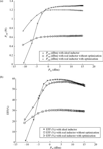
Figure 9.23: Simulation results with ideal inductors, and parasitic-laden inductors before and after optimisation
| Specification | Ideal inductors | Real inductors | |
|---|---|---|---|
| | |||
| without optimisation | with optimisation | ||
| | |||
| Input power | 0 dBm | 0 dBm | 0 dBm |
| Output power | 1.2W | 0.6W | 1.2W |
| Gain (@ Pin = 5 dBm) | 30 dB | 27 dB | 30 dB |
| Drain efficiency | 58% | 30% | 55% |
Clearly, the parasitics of the passive components significantly degrade the performance of the power amplifier by effectively de-tuning it. Also, Figure 9.23 shows the simulation results with parasitic-laden inductors after parasitic-aware optimisation. As illustrated, parasitic-aware RF synthesis is essential in the design of efficient high-performance RF circuits that are robust to process, temperature and voltage variations. As summarized in Table 9.3, the use of CAD optimisation significantly improves circuit performance; the final design including passive parasitics meets the original design specifications.
9.4.3 CMOS RF distributed amplifiers
The four-stage distributed amplifier shown in Figure 9.24 employs two artificial LC delay lines. One, called the gate line, applies delayed versions of the input RF signal sequentially to the four gate terminals [11, 12]. The other, the drain line, adds the drain signal currents constructively in the load resistor. Cascode transistors are used to reduce the Miller effect by imposing low impedance at the drains of the amplifying devices. Cascoding also reduces capacitive coupling between the artificial transmission lines and increases gain flatness, reverse isolation, stability and input and output impedance matching accuracy. The high output impedance of the cascode configuration also reduces loss associated with amplifier loading on the drain line.
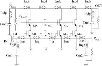
Figure 9.24: Four-stage CMOS distributed amplifier with artificial LC gate and drain delay lines
An LC transmission line exhibits an intrinsic mismatch at each termination point due to image impedance variations with frequency. Hence, m-derived half-sections are inserted to improve the impedance matches to the delay lines.
In order to increase gain flatness and decrease gain peaking near the cut-off frequency, a staggering technique is frequently used in distributed amplifiers. Staggering basically means adopting slightly different cut-off frequencies for each delay line in order to increase the overall linearity of phase response. Specifically, designing the gate line to have a slightly higher cut off improves gain flatness. Assuming matched impedances at the input and output ports of the distributed amplifier, the cut-off frequency, characteristic impedance and low-frequency gain are:
![]()
![]()
![]()
where gm is the small-signal transconductance of the identical active devices. The n term in (9.15) indicates the unique property of gain addition in the distributed amplifier.
The technology used is a 0.35 μm CMOS process. Key amplifier specifications are a constant gain greater than 6 dB over a bandwidth greater than 6 GHz with linear phase over the full bandwidth. The input and output ports are matched to 50 Ω, and the distributed amplifier operates from a single 2.5 V power supply.
In the distributed amplifier, 11 design parameters are optimised with a cost function given by
![]()
where weight_gain and weight_DIFF are weight functions of gain and DIFF terms.
According to equation (9.16), the gain needs to be greater than 2 (6 dB), and the difference (DIFF_gain) between maxgain and mingain needs to be less than 0.6. In this simulation, weight_gain and weight_DIFF are 50.
9.4.4 Distributed amplifier optimisation results
Figure 9.25 shows the comparison between simulated annealing and adaptive simulated annealing with tunnelling algorithms. Because there are only 11 design parameters to be optimised in this distributed amplifier, both methods find the solution within 5,000 iterations. Yet, as shown previously in the power amplifier case, adaptive simulated annealing finds the solution with fewer iterations than simulated annealing. As shown in Figure 9.26, the local optimisation and tunnelling techniques save a substantial number of iterations.
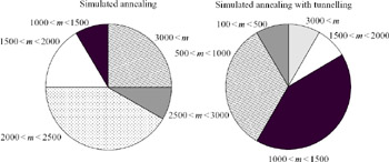
Figure 9.25: The number of iterations required to find the optimum solution for simulated annealing without and with tunnelling (12 synthesis runs) for the distributed amplifier
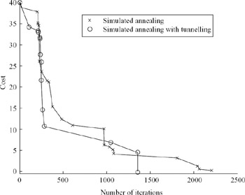
Figure 9.26: Cost functions versus the number of iterations in conventional and adaptive simulated annealing with tunnelling
Table 9.4 shows the design parameter values identified in Figure 9.24 before and after optimisation. As shown, many inductors and capacitors become smaller because the design now takes advantage of their parasitics as part of the design process.
| Value | Ideal | After optimisation |
|---|---|---|
| | ||
| Ingp | 0.743 nH | 0.23 nH |
| Indp | 1.06 nH | 0.73 nH |
| Ings | 1.114 nH | 1.273 nH |
| Ing | 1.39 nH | 1.59 nH |
| Inds | 1.59 nH | 1.77 nH |
| Indd | 1.99 nH | 2.68 nH |
| Cd | 600 fF | 186 fF |
| Cm1 | 167 fF | 144 fF |
| Cm2 | 167 fF | 431 fF |
| Cm3 | 239 fF | 713 fF |
| Cm4 | 239 fF | 0 fF |
As was the case with the power amplifier, Figure 9.27 and Table 9.5 also show an intolerable degradation in distributed amplifier performance when the ideal inductors are replaced by their parasitic-laden counterparts: the bandwidth decreases to about 2 GHz, the gain drops to 3 dB, and the flatness of the gain characteristic is lost. In this example, parasitics adversely affect the final design because they were not considered early in the design phase. Conversely, the parasitic-aware design methodology considers parasitics as an integral part of the synthesis process. Efficient CAD synthesis is the key enabling technology for parasitic-aware methodology.
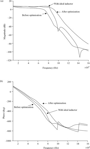
Figure 9.27: (a) Forward gain (S21(dB)) magnitude and (b) forward gain phase results
| Specification | Ideal inductors | Real inductors | |
|---|---|---|---|
| | |||
| without optimisation | with optimisation | ||
| | |||
| Bandwidth | 8.4 GHz | 7.0 GHz | 9.1 GHz |
| Average gain | 7.55 dB | 3.54 dB | 6.37 dB |
| Flatness | 0.5 dB | 3.2 dB | 0.96 dB |
|
EAN: 2147483647
Pages: 100