5.2 Filter synthesis
|
5.2 Filter synthesis
The function of the channel filter is to pass the wanted channel while rejecting neighbouring channel interferers. As these interferers occur at frequencies on either side of the passband, image responses must be suppressed and this requires using a bandpass filter with an asymmetric amplitude response, i.e. |H(jω)| ≠ |H(−jω)|. Filters of this type require complex coefficients and these can be created by polyphase networks employing two paths driven by signals which are identical but in exact phase quadrature as supplied in the down-converted I - and Q-channels of a low-IF transceiver.
5.2.1 Complex filters
The principle of the complex filter is illustrated in Figure 5.2. Starting with a real lowpass filter (i.e. with real coefficients), the transformation s → s − jω0 is applied. This shifts the poles up the imaginary axis by ω0 and transforms the lowpass response (actually a bandpass response centred at ω = 0) into an identical bandpass response centred at ω = ω0 [4]. The transformation preserves both amplitude and phase characteristics and produces the required feature of having no image response at negative frequency.
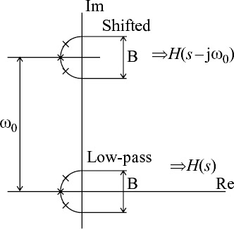
Figure 5.2: Complex filter basics
Synthesis of complex filters follows similar procedures to those for real filters except that it makes use of complex integrators. Figure 5.3 shows the signal flow graphs of real and complex current-mode integrators (voltage-mode integrators will have identical signal flow graphs).
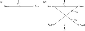
Figure 5.3: Ideal integrator signal flow-graphs: (a) real, (b) complex
The real integrator has an input iin and an output iout, and a transfer characteristic described by
![]()
where τ is the integrator time constant.
The complex integrator has two inputs iin1 and iin2 where iin2 = j iin1, two outputs iout1 and iout2 and two extra outputs −α0 iout1 and α0 iout2 fed back to the inputs where they sum with iin2 and iin1 respectively. We can demonstrate that this is the required signal flow graph from its nodal equations which are
![]()
![]()
Combining these equations, the transfer characteristics for the two paths are
![]()
![]()
So, H1(s) = H2(s) = H(s) and the outputs iout1(s) and iout2(s) are identical but in phase quadrature. For α0 = ω0τ,
![]()
which demonstrates that the transformation, s → s − ω0τ, is being performed as required by the complex integrator.
The physical implementation of a complex filter is determined by the chosen integrator realisation. Traditionally, continuous-time RC-active integrators [5] using passive resistors and capacitors, and operational amplifiers or special buffers [6], are employed. However, it will be difficult to maintain their excellent performance as we use lower supply voltage CMOS processes. Sampled-analogue integrators using switched capacitors [7] or switched currents [8] may also be employed. Switched capacitors will also lose performance in low-voltage CMOS and, being sampledanalogue, require additional anti-alias filters. Switched currents [8] also require additional anti-alias filters but their performance is not expected to degrade at lower supply voltages [9].
Here the plan is to use the Gm-C technique and Figure 5.4 shows current-mode integrators for use in our Gm-C filters. The real integrator input current flows into the capacitor C to develop an input voltage vin(s) = iin(s)/sC which produces an output current iout(s) = G vin(s) = iin(s) G/sC. The transfer function is H(s) = G/sC which describes a real integrator with a time constant τ = C/G. The complex integrator is developed directly from its signal flow graph and the feedback signals are produced by the cross-branch transconductors G0 and −G0 where G0 = α0 G. The frequency shift ω0 is given by
![]()
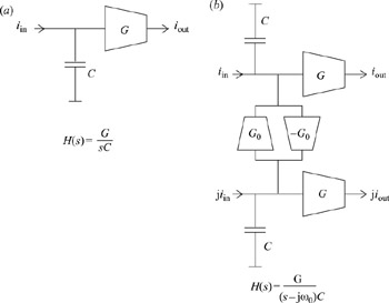
Figure 5.4: Current-mode Gm-C integrators: (a) real, (b) complex
5.2.2 Bluetooth filter synthesis
We can now proceed to synthesise the complex filter. First, we generate the lowpass real filter by traditional leapfrog methods and then the complex bandpass filter is created by shifting the real lowpass response to the required centre frequency. We will create a fifth-order 0.5 dB equiripple Chebyshev complex leapfrog channel filter suitable for Bluetooth, using the Gm-C current-mode integrators described in the previous section.
The synthesis starts with the lowpass LCR prototype shown in Figure 5.5a. Its nodal equations are:
![]()
![]()
![]()
![]()
![]()
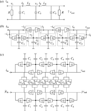
Figure 5.5: Channel filter architecture: (a) fifth-order LP prototype; (b) Gm-C LP filter; (c) Gm-C complex bandpass filter
Using traditional signal flow graph methods, the Gm-C filter structure shown in Figure 5.5b is constructed which simulates the nodal equations of the prototype using state variables v1, i2, v3, i4 and v5. The specific current integrators are shown boxed.
Translating this lowpass design into its complex bandpass counterpart involves providing two paths, each containing the lowpass filter, and then replacing the real integrators with complex integrators. This results in the architecture shown in Figure 5.5c. The design values for the Bluetooth channel filter response (F0 = 1 MHz, BW = 1.2 MHz) are given in Table 5.1.
| Parameter | Value |
|---|---|
| | |
| G | 40 μS |
| G11 | 113.72 μS |
| G22 | 81.97 μS |
| G33 | 169.39 μS |
| G44 | 81.97 μS |
| G55 | 113.72 μS |
| C1 | 18.10 pF |
| C2 | 13.05 pF |
| C3 | 26.96 pF |
| C4 | 13.05 pF |
| C5 | 18.10 pF |
It can be seen from Figure 5.5c that the various transconductor loops are in fact gyrators [10]. Figure 5.6 shows a gyrator view of the channel filter. The circuit clusters at C2 and C4 are gyrator-C equivalents for the inductors L2 and L4. Furthermore, the cross-branch transconductor loops which produce the frequency shift are also gyrators which produce fixed negative susceptances of −jω0Cn at each capacitor Cn. The capacitor set is transformed from Cn to (s − jω0)Cn which again explains the frequency shift.
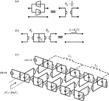
Figure 5.6: Gyrator view of channel filter: (a) gyrator–transconductor equivalence; (b) gyrator-C inductor; (c) channel filter
A balanced version of the channel filter is shown in Figure 5.7 and the design values of its differential transconductors and floating capacitors are half of those of the single-ended design given in Table 5.1. Using idealised transconductors and capacitors, the simulated idealised amplitude response is shown in Figure 5.8 and the idealised passband amplitude and group delay responses are shown in Figure 5.9.
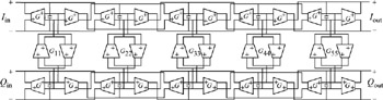
Figure 5.7: Balanced channel filter
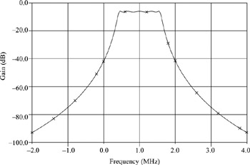
Figure 5.8: Ideal amplitude response of balanced channel filter
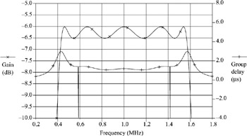
Figure 5.9: Ideal amplitude and group delay responses of balanced channel filter
|
EAN: 2147483647
Pages: 100