2.8 Incorporation in a dual-mode receiver
|
2.8 Incorporation in a dual-mode receiver
The low-IF architecture as described with its non-complex signal processing is a practical proposition for use with GSM and other such narrowband, FDMA/TDMA radio standards where a spread-spectrum air interface is not a feature. Depending upon the physical implementation, it could offer a modest saving in power consumption of the order of 17 per cent. However, by far the most important factor in its favour is the added flexibility that it can give to a highly digitised, multimode receiver that must operate with both spread-spectrum and non-spread-spectrum RF signals.
An illustration of how the modified, low-IF architecture can be incorporated in a dual-mode receiver is given in Figure 2.19. This particular receiver [13] is intended to operate in UMTS and GSM modes but is adaptable enough to accommodate other modes like CDMA2000 should this be necessary. It should be noted that there is a difficult design problem to be addressed in making the RF frontend cope with the multiple frequency bands that are encountered with the different modes. This is something of a separate problem from the design of the IF and baseband parts of the receiver but nonetheless is one that must be solved. For the rest of the receiver, however, the most important design issues relate to cost, complexity and power consumption. These translate into the need for an architecture comprising a minimum number of common hardware and software blocks which can be both re-used and reconfigured for use in all of the different modes. As previously explained, reconfiguration is generally easier if the majority of the blocks are digital in nature (see the forward location of the ADC(s) in the diagram). Re-use and reconfiguration were central principles behind the creation of the architecture of Figure 2.19 and the incorporation of the non-complex IF processing.
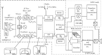
Figure 2.19: Dual-mode UMTS/GSM receiver architecture
With reference to Figure 2.19, the two dotted outlines indicate the respective grouping of blocks used for the UMTS and GSM modes. Most of the blocks between the RF frontend and the baseband signal processing parts have been re-used and even some of the baseband parts, shown separate in the figure, could be implemented on a common processor core. Depending upon the multiband capability of the RF frontend, one or more quadrature pairs of mixers would translate the incoming signals down to a zero-IF for UMTS and a low-IF of 100 kHz for GSM. The subsequent AC couplings which have a cut-off frequency of 10 kHz to suit GSM, can stay in place for UMTS without causing any detrimental effect. Similarly, the lowpass pre-filters which have a cut-off frequency of 8.5 MHz to suit UMTS, can stay in place for GSM. The IF pre-amplifiers shown have three gain settings constituting a small amount of AGC. Two of the steps are required to cope with the full extent of the dynamic range of the UMTS signals and are selected on the basis of the power detected at the output of the digital channel filters. The third gain setting simply ensures that the different power range encountered with a GSM signal is aligned with the signal-processing window of the single ΣΔ modulator. In the case of the image rejection filter, this is only required for the GSM mode and is preferably bypassed for UMTS. However, as implied by the figure, it may be possible to leave it in place for UMTS with relatively little impact on sensitivity.
Both ΣΔ modulators are active in the UMTS mode and clocked at a frequency in the region of 150 MHz. This high clock frequency is necessary to ensure the modulators cope with the increased bandwidth of a UMTS signal (i.e. in the region of 4 MHz). They are fifth-order devices with a two-level output of the type already described in Figure 2.14, the loop filter having been scaled to provide a different pair of pole frequencies. Each one feeds its own digital, FIR filter which for UMTS has a root-raised-cosine (RRC) frequency response. When operating in the GSM mode, only one of the modulators is active, the other being shut down to save power consumption. In switching from UMTS mode, the working modulator is electronically reconfigured to change its loop filter bandwidth, whilst the clock frequency is changed to 26 MHz. Its output is then fed to both digital filters, whose frequency responses are also changed to implement the make-complex and channel filtering requirements for GSM. Changing the channel filter responses is a simple matter of re-addressing the appropriate set of tap coefficients stored in local memory.
In summary, the non-complex signal processing of the sort described in this chapter can give added flexibility to a multimode receiver. In particular, it allows a single, real ΣΔ modulator to be used as an ADC in place of what would otherwise be a fully complex modulator in a conventional low-IF receiver. The benefit has been demonstrated in the receiver structure shown in Figure 2.19, wherein operation in UMTS mode favours a zero IF and operation in GSM mode a low IF. Not only does this allow the same basic ΣΔ modulator to be used for both modes but it substantially simplifies the design of the modulator, already made difficult by the performance requirements of UMTS.
|
EAN: 2147483647
Pages: 100