10.3 Direct Sequence Spread Spectrum
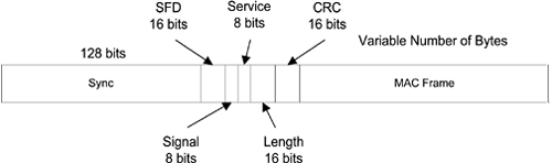
| In this section, features of the DSSS wireless Ethernet are highlighted by examining the packet structure, the 11-bit Barker code modulation process, and the spectrum mask. 10.3.1 Summary of DSSS StandardsThe packet format for the DSSS implementation of wireless Ethernet is shown in Figure 10.17. A DSSS packet consists of a preamble, a header, and a MAC frame. The DSSS preamble has a Sync field of 128 bits and a Start Frame Delimiter of 16 bits. The DSSS header has a Signal field of 8 bits, a Service field of 8 bits, a Length field of 16 bits, and a CRC field of 16 bits. Figure 10.17. DSSS Packet Format
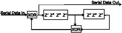
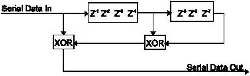
The DSSS preamble Sync field contains 128 bits of scrambled 1s to be used by the receiver to detect a signal and to achieve frequency and timing synchronization with the rest of the received packet. The SFD consists of the binary pattern of 1111 0011 1010 0000 used for start of frame indication. The SFD least significant bit (lsb) is transmitted first in time. The Signal field indicates the modulation rate used for the MAC frame. The data rate equals the Signal field value multiplied by 100 kbps (i.e., 0000 1010 for 1 Mbps and 0001 0100 for 2 Mbps). The Service field is reserved for future use. The value 0000 0000 signifies compliance. The Length field indicates the number of microseconds, up to 216 1, required to transmit the MAC frame. The Length lsb is also transmitted first in time. The CRC is a frame check sequence generated against Signal, Service, and Length fields using the same Comite Consulatif International Telephonique et Telegraphique (CCITT) CRC-16 polynomial of G(x) = x16 + x12 + x5 + 1. All bits in a DSSS packet are scrambled with a self-synchronizing scrambler based on the generator polynomial of G(z) = z-7 + z-4 + 1. Figure 10.18 shows a possible way of implementation using delay elements and exclusive OR operations. The scrambler can be initialized to any state except all 1s when transmitting. Figure 10.19 shows a possible implementation for the descrambler. Figure 10.18. A Self-Synchronizing Scrambler Realization (From IEEE Std. 802.11. Copyright © 1999 IEEE. All rights reserved.)
Figure 10.19. A Self-Synchronizing Descrambler Realization (From IEEE Std. 802.11. Copyright © 1999 IEEE. All rights reserved.)
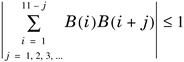
Within the 2.4-GHz IMS band, there are 11 carriers that are 5 MHz apart, allocated by the FCC for U.S. and Canada DSSS operations starting at 2.412 GHz. To minimize interference, coexisting carriers need to be 30 MHz apart. Therefore, at least two separate DSSS wireless Ethernets can coexist at the same location. Starting from the MAC frame, each bit, for 1 Mbps, or each pair of bits, for 2 Mbps, are modulated to the radio carrier frequency at a rate of 1 million symbols per second. For the MAC frame, each symbol carries 1 or 2 bits for 1 Mbps or 2 Mbps, respectively. On the other hand, each symbol consists of 11 chips corresponding to the 11-bit Barker code of +1 1 +1 +1 1 +1 +1 +1 1 1 1. In other words, the bandwidth-related signaling rate is effectively 11 Mega-chips per second (Mcps). Because of the use of this Barker code, the spectrum of the DSSS wireless Ethernet becomes 11 MHz, even though the symbol rate is only 1 MHz. The Barker code is used because of its very high peak autocorrelation value when aligned for further SNR enhancement at the receiver. Let the Barker code be B(k), we have Equation 10.7
and Equation 10.8
For 1 Mbps, a 1 bit is represented by the original Barker code, or 0 phase, and a 0 bit is represented by the sign reversal of the Barker code, or a p shift. For 2 Mbps, bit combinations of 00, 01, 11, and 10 are represented by 0, p/2, p, and p/2 phase shifts of the Barker code, respectively. p/2 and p/2 phase shifts are implemented using in-phase and quadrature channels of Figure 10.20. Barker Code Power Spectrum and DSSS PSD Mask (From IEEE Std. 802.11. Copyright © 1999 IEEE. All rights reserved.)
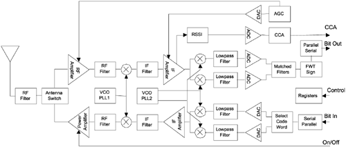
10.3.2 DSSS Transceiver Architecture and Performance EstimationFigure 10.21 shows a functional block diagram of a typical DSSS wireless Ethernet transceiver. There are two PLL-controlled local oscillators: VCO/PLL2 for the IF of about 100 MHz and VCO/PLL1 for the choice of a particular DSSS carrier. In the transmit path, bits or bit pairs are encoded into Barker code symbols. Barker code symbols are separately converted to analog formats for in-phase and quadrature channels. After low-pass filtering, symbols are modulated and combined in the IF. Complex IF symbols are then modulated to RF, amplified, and sent to the antenna for transmission. In the receiving path, the RF signal from antenna is amplified and then demodulated to IF. After additional amplification, IF symbols are demodulated to baseband of separate in-phase and quadrature channels. After low-pass filtering, baseband symbols are converted to digital formats. Digital symbols in the format of Barker code chips are despreaded for SNR enhancement. Enhanced symbols are then decoded into bit streams. The operation of a DSSS transceiver is half-duplex, and local oscillators are used for either transmit or receive. Because the amplitude information of DSSS symbols is very important, received signal strength is monitored at both the IF amplifier and the analog-to-digital convertor (ADC) stages. RF and IF amplifier gains are adjusted to maintain proper signal level at analog-to-digital outputs for further signal processing. Received signal strength indication is used for both Clear Channel Assessment (CCA) and Automatic Gain Control. Figure 10.21. DSSS Transceiver Structure
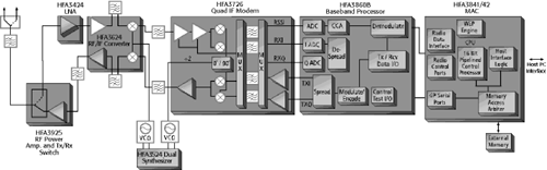
To transmit, the CCA is first checked. The transceiver microcontroller then assembles a packet in the right format, turns on the transmit path circuits, and sends the packet as a bit stream through the encoder. The transceiver is normally in the receive mode to monitor the presence of any packet in the RF medium. After the RF energy is indicated by CCA, the transceiver adjusts its gain level and tries to catch the Start Frame Delimiter. If the SFD is detected, CRC bits are checked before the rest of the packet is collected to be sent to the transceiver microcontroller for data recovery. Meanwhile, timing information is also derived from the preamble for proper adjustment for recovery of the rest of the packet. Figure 10.22 shows an example of a DSSS transceiver chip set from Intersil. This chip set consists of a MAC part, a baseband processor, an IF modem, an RF/IF convertor, an LNA, and a PA. The MAC part is based on a 16-bit ARM core with control and MAC firmware residing on external memory. The ARM core is a RISC (Reduced Instruction Set Computer) microcontroller. The MAC part uses dedicated circuits for WEP processing. The MAC part also contains a host interface to a PC or other devices, a radio control interface, and a digital serial interface to write to or read from registers on other chips. The baseband processor contains in-phase and quadrature channel ADCs, an RSSI ADC, and demodulation and modulation circuits. The IF modem contains in-phase and quadrature channel digital-to-analog convertors (DAC), IF modulation and demodulation circuits, and IF amplifiers. The RF/IF convertor contains RF amplifiers and RF modulator and demodulators. This chip set needs two external oscillators, RF and IF bandpass filters, and some memory chips to form a DSSS transceiver. Figure 10.22. A DSSS Chip Set Example
The transmit power of a DSSS transceiver is defined to be between 0 and 30 dBm. A DSSS transceiver needs to operate under the received signal level of 4 dBm when transceivers are close by. The receive sensitivity is also required to be 80 dBm for the 2-Mbps DQPSK modulation. The allowed signal attenuation is between 80 and 110 dB. The maximum operable distance between transceivers could exceed 2000 ft at the 30-dBm transmit power level in a barrierless transmission environment. On the other hand, the receiver front-end noise level Pnoise can be calculated according to the input resistor thermal noise level PR = kT = 174 dBm/Hz, the antenna and amplifier noise figure NF = 14 dB, and signal bandwidth B = 11 x 106. We have Equation 10.9
At a signal-to-noise level of about 9.59 dB, the channel capacity for the DSSS environment is Equation 10.10
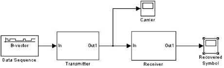
The transmission performance of a DSSS wireless Ethernet transceiver can be further studied by computer simulation. Figure 10.23 shows a simplified Simulink model consisting of a random data sequence generator, a transmitter, and a receiver. Figure 10.23. A Simulink DSSS Simulation Model
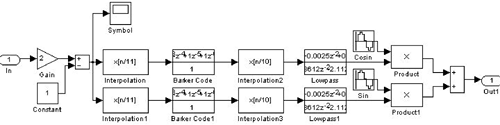
Figure 10.24 shows the internal structure of the Simulink transmitter model. Binary data sequence is first converted into symbols of ±1 levels. For this assumed 1-Mbps throughput, the same data symbol is sent through both in-phase and quadrature channels. The symbols are spread to a chip rate of 11 MHz by an interpolation and Baker code filters. The sampling rate is further increased to 110 MHz by another interpolation filter for subsequent low-pass filtering and modulation processes. These two fourth-order Butterworth low-pass filters have corner frequencies of 5.5 MHz. They might be realized with analog circuits in a real implementation. The low-pass filtered Baker code chips are modulated with cosine and sine waves of a carrier. The carrier frequency for this Simulink model is 11 MHz. Again, the carrier might come from a VCO in a real implementation. Figure 10.24. The Simulink DSSS Transmitter Model
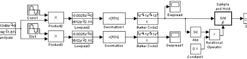
Figure 10.25 shows the internal structure of the Simulink receiver model. The received signal is first bandpass-filtered to minimize out-off-band noise. This second-order Butterworth bandpass filter has corner frequencies at 5.5 and 16.5 MHz. The bandpass-filtered signal is demodulated with cosine and sine waves of an 11-MHz carrier. In-phase and quadrature baseband channels are also recovered after low-pass filtering by low-pass filters of the fourth order. Low-pass filtered signals are decimated to 11 mega samples per second for despreading by Barker code filters. Peaks are then registered to recover data symbols. Figure 10.25. The Simulink DSSS Receiver Model
|
 10.4 dB. The DSSS wireless Ethernet transmit power resulting from the 11-Mcps Barker code is defined to be between 1 and 1000 mW. With a bandwidth of 11 MHz, the PSD level is between 70 and 40 dBm/Hz. The unfiltered power spectrum resulting from the Barker code and the spectrum mask defined by the standards are shown in Figure 10.20. Additional low-pass, at Barker code, or bandpass, at IF or RF, filtering is required to meet the mask requirement.
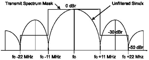
EAN: 2147483647
Pages: 97