4.5 Data Access Instructions
| We now discuss data access using the Itanium load and store instructions, concentrating on simple integer data. As we mentioned in Chapter 2, modern computer designs almost invariably have a memory subsystem that is supplemented by cache structures designed to shorten access times. For some architectures, the presence and nature of cache structures are left entirely to implementation. Cache is then not a concern of architecture, since there is no way to interact with cache structures through the instruction set. One can only observe the effect of the cache by comparing the execution times of a benchmark program on systems that have or that lack particular cache structures. For other architectures, especially Itanium architecture, the presence and nature of cache structures are intrinsic to both architecture and implementation. Ways to sense the presence or absence of cache structures and influence their behavior are included in the ISA. Those instructions might be privileged (i.e., of use only within system software), or they might be available to user-level processes. 4.5.1 Itanium Cache StructuresThe Itanium architecture specifies that cache structures be explicitly visible to the assembly language programmer and the compiler writer. Table 4-3 gives a simplified view of memory hierarchy using the quantitative details for the Itanium 2 processor. The line size for a cache specifies the granularity with which data move between a cache level and higher-numbered levels or main memory. For example, the L3 cache always reads 128 bytes from main memory or copies back 128 bytes to main memory. The line size does not preclude moving smaller quantities of data into or from the CPU.
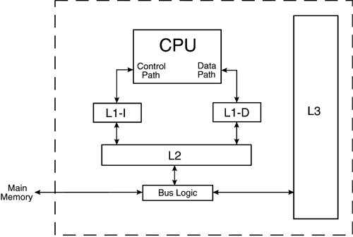
Cache structures improve access to data at the expense of greater cost of implementation. For the Itanium 2 processor, the L1, L2, and L3 cache structures are all on the main processor chip. Chapter 13 details the differences in cache structure for the original Itanium processor. (Refer to hardware organization books for explanations of cache replacement and cache write policies.) Figure 4-4 shows the relationships among the components of the memory hierarchy for an Itanium 2 system. The L3 cache structure is attached to a separate bus in a manner that is sometimes called backside cache. The box labeled Bus Logic permits the L3 cache to monitor and reflect data access activity of the L2 cache and to retain a longer history of that activity. Figure 4-4. Itanium 2 system cache relationships
The history of computers has given us two methods for generic memory organization. The von Neumann architecture, as implemented in a very early computer at the Institute for Advanced Study (Princeton, NJ), has one general-purpose memory structure that flexibly accommodates both instructions and data. The Harvard architecture, idealized from another very early computer designed at Harvard University (Cambridge, MA), has separate memories of fixed sizes for instructions and data. Most contemporary systems are designed using von Neumann's principles, but may have Harvard-style structures at the innermost (L1) cache. With RISC and EPIC designs having many registers, sequences of instructions should be able to work with data already retrieved by the CPU. A separate read-only cache for instructions (L1-I) can have a different design from a read/write cache for data (L1-D), and their separate connections to the control and data paths of the CPU can be kept short. Table 4-3 shows timing differences because the Itanium 2 processor connects floating-point data only to the L2 cache structure. Hence only integer and logical operations, which are more prevalent, benefit from the L1-D cache structure. Even code that performs floating-point operations uses integer quantities to implement pointers and counters. Compared to caches in other contemporary designs, the innermost (L1, L2) Itanium cache structures are not especially large. The Itanium ISA provides ways to optimize utilization of the cache structures by prefetching a line of data that will soon be needed by a program into the cache structures or, conversely, by flushing a line of data that the program no longer needs back into main memory. In addition, the CPU attempts to prefetch the instruction stream into the L1-I cache. The integer store and load instructions, discussed next, use instruction completers i.e., extensions of the opcode mnemonics that are translated into various subcode fields within the machine instructions. One sort of completer for a load or store instruction provides hints to the cache structures. The integer arithmetic instructions, which we discussed earlier in this chapter, do not have completers. 4.5.2 Integer Store InstructionsThere are two kinds of integer store instructions for Itanium architecture, the normal form and the spill form, having the following assembler syntax: stsz.sttype.sthint[r3]=r2 // mem[r3] <- r2 stsz.sttype.sthint[r3]=r2,imm9 // mem[r3] <- r2 // r3 <- r3 + sext(imm9) st8.spill.sthint[r3]=r2 // spill data and NaT bit st8.spill.sthint[r3]=r2,imm9 // spill data and NaT bit // r3 <- r3 + sext(imm9) where sz is the size of the information unit in memory into which the lowest-order 1, 2, 4, or 8 bytes of the quantity in register r2 are to be copied by the normal form to the memory hierarchy at the address specified in register r3. The simplest store instruction uses register direct addressing for the source operand and register indirect addressing for the destination operand. Store operations can be susceptible to hardware-detected exceptions. Chief among those would be an attempt to store unaligned data. If we want to store 1, 2, 4, or 8 bytes, we must ensure that the lowest 0, 1, 2, or 3 bits in the address expressed in register r3 are zero. There are two values for sttype (the store type completer): none at all and rel. None at all corresponds to an ordinary store operation, and rel corresponds to an ordered store performed with release semantics that we shall not discuss further. There are two values for sthint (the store hint completer): none at all and nta. None at all corresponds to an ordinary store operation; the processor hardware then assumes that the program associates temporal locality in the L1 cache with the value stored. On the other hand, nta provides the hint that the program considers the value stored to have nontemporal locality at all levels of cache and memory. The use of nta may thus avoid knocking out of the caches some other data that may be reused. The Itanium store instructions provide for postmodification of the value in the pointer register r3 by a signed adjustment ranging from 256 to +255 address units. Many other architectures provide an addressing mode known as autoincrement, where the pointer register is typically postincremented only by the byte size of data copied. Some architectures also offer an autodecrement addressing mode, though that situation is usually defined as a predecrement, not a postdecrement as here. The spill form always copies 8 bytes, along with a validity bit associated with register r2. The spill form is used to save register contents when an operating system switches context from one process to another or an application uses a preserved register. 4.5.3 Integer Load InstructionsThere are two kinds of integer load instructions for Itanium architecture, the normal form and the fill form, having the following assembler syntax: ldsz.ldtype.ldhintr1=[r3] // r1 <- mem[r3] ldsz.ldtype.ldhintr1=[r3],r2 // r1 <- mem[r3] // r3 <- r3 + r2 ldsz.ldtype.ldhintr1=[r3],imm9 // r1 <- mem[r3] // r3 <- r3 + sext(imm9) ld8.fill.ldhintr1=[r3] // fill data and NaT bit ld8.fill.ldhintr1=[r3],r2 // fill data and NaT bit // r3 <- r3 + r2 ld8.fill.ldhintr1=[r3],imm9 // fill data and NaT bit // r3 <- r3 + sext(imm9) where sz is the size of the information unit in memory at the location specified by register r3 from which 1, 2, 4, or 8 bytes are to be copied into the lowest-order 1, 2, 4, or 8 bytes of register r1 by the normal form. The upper-order 7, 6, 4, or 0 bytes of register r1 are zeroed put another way, the loaded data are zero-extended to a full 64 bits in width and then placed in register r1. The simplest load instruction uses register indirect addressing for the source operand and register direct addressing for the destination operand. Load operations can be susceptible to numerous hardware-detected exceptions. Chief among those would be an attempt to load unaligned data. If we want to load 1, 2, 4, or 8 bytes, we must ensure that the lowest 0, 1, 2, or 3 bits in the address expressed in register r3 are zero. There are several values for ldtype (the load type completer). None at all corresponds to an ordinary load operation. Other values correspond to an ordered load, a biased load, a speculative load, and/or an advanced load. We shall consider the advantages and potential drawbacks of speculative and advanced load instructions in a later chapter. There are three values for ldhint (the load hint completer): none at all, nt1, and nta. None at all corresponds to an ordinary load operation; the processor hardware is given the hint that the program associates temporal locality in the L1 cache with the value loaded. At the other extreme, nta provides the hint that the program considers the value loaded to have nontemporal locality at all levels of cache and memory, while nt1 provides the hint that the program considers the value loaded to have nontemporal locality in just L1 cache. The use of nta may thus avoid knocking out of the caches some other data that may be reused. The use of nt1 may avoid knocking out of L1 cache some other data that may be reused, but suggests defensively that the data loaded may need to be requested from L2 or L3. Like the Itanium store instructions, the load instructions provide for postmodification of the pointer value in register r3 by a signed amount, which can range from 256 to +255 address units (immediate constant) or can be a full 64-bit signed amount (in register r2). The fill form always copies 8 bytes along with a validity bit associated with register r1. The fill form is used to restore register contents when an operating system switches context from one process to another or an application uses a preserved register. 4.5.4 Move Long Immediate InstructionAddress pointers are essential for instructions that perform store and load operations. In RISC and EPIC architectures, the instructions that use such pointers expect a pointer value to be already loaded in a register. We have seen how the mov pseudo-op can place an integer into a register, but the width of that integer is limited to the 22 bits of immediate data that can be encoded into an underlying addl instruction. The SQUARES and HEXNUM programs have already shown one way around that limitation. In those programs, we used capabilities of the assembler and linker to develop addl instructions containing a signed 22-bit offset from the value in a global pointer register. That method works so long as the total amount of data that we need to reach does not exceed the relative addressing capability of 22 bits (4 MiB). Otherwise, another pointer register may be needed to span the address range for the data. What could be a more general approach? One answer would be an instruction that would load a full-width address value as immediate data from the instruction stream into a general register. Itanium architecture provides a special instruction called movl that can accommodate a full 64-bit immediate value: movl r1=imm64 // r1 <- imm64 movl r1=label // r1 <- 64-bit address for label where the 64-bit immediate value, or the full 64-bit address finally determined by the linker for a label, is copied into the general register r1. Unlike the addl instruction that restricted source register r3 to be Gr0 Gr3, the movl instruction can put the value into any general register, Gr1 Gr127. This instruction provides a complete solution to the challenge of full-range addressing. The 64-bit immediate value fits into unused space in one instruction slot and the next entire instruction slot; thus, movl occupies two slots in a 128-bit instruction bundle and must be decoded for execution as a special case. Since Itanium assemblers permit the 64-bit immediate value to be specified symbolically, we now have another method for setting up pointers for store and load operations. For instance, in HEXNUM, we could replace the lines: addl r14 = @gprel(H1),gp;; // Point to storage ld8 r21 = [r14];; // for 1st hex digit with the lines: movl r14 = H1;; // Point to storage ld8 r21 = [r14];; // for 1st hex digit but not with the lines: mov r14 = H1;; ld8 r21 = [r14];; which would not assemble and link successfully because the mov pseudo-op would only generate an adds or addl instruction (see Section 4.2.4), and the true address determined by the linker for H1 would be wider than 14 or 22 bits. 4.5.5 Accessing Simple Record StructuresApplication data can be composed of numerous records, each having an identical internal structure, in the form of fields of information. It is important to learn how an architecture can access such data most conveniently. Consider the fictitious situation of a company that makes 40 kinds of widgets. The company's general manager tracks the cost of manufacture, the selling price, the shipping cost, and current inventory for each kind of widget. For simplicity, suppose that each piece of numeric information about the widgets is stored as a quad word integer. The same fields of information would occur for each of the 40 kinds of widgets, and it makes sense to store those fields in the same order for each kind of widget. This can be done by defining address offsets as symbolic displacements: MODEL = 0 COST = 8 PRICE = 16 FREIGHT = 24 STOCK = 32 RECSIZE = 40 In a program, one register can be stepped along by the total record size (here, 40 bytes), and the offsets will then specify each field. For example, the total cost of manufacture of all the widgets in the inventory can be computed schematically as follows: movl r14 = TABLE-RECSIZE;; // Pre-index for data mov r20 = 0;; // Value accumulator loop: adds r14 = RECSIZE,r14;; // Point to next record adds r15 = COST,r14;; // Set pointer ld8 r21 = [r15];; // to get cost adds r15 = STOCK,r14;; // Set pointer ld8 r22 = [r15];; // to get quantity <now need to multiply: r23 = r21 * r22> add r20 = r23,r20;; // Running value <goto loop if not at end of table> done: <print report using r20 as value of inventory> where TABLE is an address label for the start of the data. The address pointer (r14) is incremented at the top of the loop, even for the first traversal, and thus must be preindexed to the address value given by the symbolic expression TABLE RECSIZE. The addressing technique here is limited to a RECSIZE that does not exceed the capacity of an immediate value for the adds instruction. We have not attempted to provide details for the actual multiplication, loop control, or printing. The capability of the assembler to handle symbolic offsets and address subtraction has allowed us to write a readable and maintainable program. Moreover, only two general registers are needed to handle addressing details: one to point to records and the other to point to fields within records. 4.5.6 Access to Specialized CPU RegistersIn keeping with EPIC principles, the Itanium architecture provides the programmer with access to many internal resources of the processor, since more compile-time as well as runtime decisions are necessary to exploit the full power of EPIC features than has been necessary for CISC or RISC architectures. In addition to large numbers of registers used in calculations involving integer and floating-point data, an Itanium processor includes many specialized register types (see Appendix D) that are tightly coupled to various processor operations. Visibility to the programmer includes the ability to copy contents between those specialized registers and general registers, using mov instructions or pseudo-ops: mov r1=reg // r1 <- contents of reg mov reg=r2 // reg <- contents of r2 mov reg=imm8 // reg <- sext(imm8) // (immediate form only for ar.xx) These instructions must execute in either M- or I-units, depending on the particular specialized resource, as tabulated in Appendix C. The instruction pointer can be read, but not modified, using a mov instruction. The form with an 8-bit immediate value as the source is only available when the destination is one of the application registers, Ar0 Ar127. We show examples of these mov instructions when needed in our sample programs; the next chapter introduces the application register called ar.lc, the loop count register. | |||||||||||||||||||||||||||||||||||||||||||||||||||||||||||||||
EAN: N/A
Pages: 223