83.
7.4 Implementation with Different Kinds of Flip-Flops
Toggle flip-flops are a natural choice for implementing binary counters, but other flip-flop types may need less hardware for implementation. Also, the availability of computer-aided design software may influence our choice of flip-flop. Existing CAD software, such as espresso, favors designs with D flip-flops, in part because D storage elements are pervasive in VLSI design. However, J-K devices often require the fewest gates to implement a given state diagram. Admittedly, as the level of integration continues to increase, saving a gate here or there becomes less of an issue.In Section 7.2.2 you saw how to implement the five-state up-counter of Figure 7.18
(state transition diagram) and Figure 7.19 (state transition table) using toggle flip-flops. In this section, you will see three more implementations of this counter, using R-S, J-K, and D storage elements.7.4.1 Implementation with R-S Flip-Flops
We already performed the first three steps of the counter design procedure-the state transition diagram, the state transition table, and the next-state K-map-in Section 7.2.2(see Figures 7.18, 7.19, and 7.20). Step 4, remapping the next state functions into control inputs for the chosen flip-flop, is the one step that depends on the type of flip-flop selected. R-S Excitation Table We start with the excitation table for the R-S flip-flop, which is given in Figure 7.28.

The state transitions are now encoded in terms of the R and S inputs that cause the flip-flops to make those transitions. For example, if the flip-flop's current state is 0 and the next state is also to be 0, we can accomplish this by setting the S input to 0 and the R input to either 0 (hold current state) or 1 (reset current state). We complete the remaining three entries of the tables in a similar manner.
Remapped State Transition Table The next step is to reexpress the state transition table in terms of the R and S inputs to the three state flip-flops C, B, and A. This is shown in Figure 7.29.
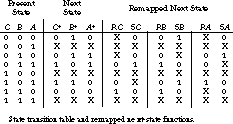
We complete the remapped state transition table as follows. First we examine how the state bit is to change-for example, from a 0 to a 1. We use this information and the R-S excitation table to determine the R and S inputs needed to make that transition happen. We repeat the procedure for each state bit (column) and each state transition (row) of the state transition table.
Let's see how we obtained the table of Figure 7.29. In the transition from state 000 to 010, C changes from 0 to 0, B from 0 to 1, and A from 0 to 0. The A and C transitions are implemented by the R and S inputs X and 0. The 0-to-1 transition for B is accomplished by setting R and S to 0 and 1, respectively. For the state transition 010 to 011, C goes from 0 to 0, B from 1 to 1, and A from 0 to 1. Based on the excitation table, C's R and S inputs should be X and 0, B's inputs are 0 and X, and A's are 0 and 1. We determine the rest of the transitions in a similar -manner.
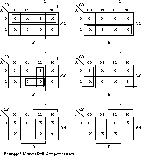
Remapped K-maps and Counter Schematic Figure 7.30 shows the re-mapped K-maps. The minimized next-state functions
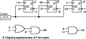
This implementation requires 4 gates and 10 literals. If we factor the expression for RB, that is, RB = B(A + C), we can save another gate and a literal. The implementation logic is shown in Figure 7.31: 3 gates, 9 -literals, and a total of 12 wires if we consider the flip-flop inputs. We do not count the clock in this tabulation. The figure doesn't show the reset logic.
7.4.2 Implementation with J-K Flip-Flops
The first three design steps are exactly as in the previous subsection. The only difference is that we now use the excitation table for the J-K flip-flop. This is shown in Figure 7.32. For a transition from a current state of 0 to a next state of 0, the J input should be set to 0 and the K to 0(hold) or 1 (reset). In a 0-to-1 transition, J should be set to 1 with K at 0 (set) or 1 (toggle). We handle the 1-to-0 transition and 1-to-1 transition similarly. 
State Transition Table and Remapped Next-State Functions The state transition table and the remapped next-state functions are given in Figure 7.33.
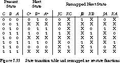
Let's examine the first two state transitions, from 000 to 010 and from 010 to 011. For the first transition C stays at 0, B toggles from 0 to 1, and A holds at 0. For this transition C's J, K inputs are 0, X (0-to-0 transition); B's inputs are 1, X (0-to-1 transition); and A's inputs are the same as C's. For the second state transition, C holds at 0, B holds at 1, and A toggles from 0 to 1. The excitation table tells us that the J, K inputs should be 0, X for C; X, 0 for B; and 1, X for A.
Remapped K-maps and Counter Schematic Because it eliminates the forbidden state, the J-K flip-flop's excitation table contains many more don't-care conditions than in the R-S case. As you would expect, this leads to an implementation with a reduced gate and literal count.
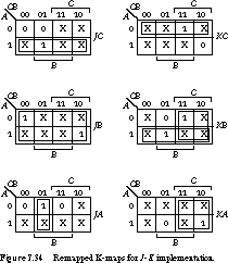
Figure 7.34 shows the K-maps for the remapped next-state functions. The reduced expressions become
This implementation reduces the gate count to two and the literals to seven. The implementation logic appears in Figure 7.35. The wire count for this implementation is nineJC =A KC=JB
=1 KB=A+C JA=BKA
=C
(we don't count the hardwired input for JB and again don't show the reset logic).There is actually little to distinguish between the R-S and J-K implementations. This should come as no surprise, given the similar behavior of these two types of devices.
7.4.3 Implementation with D Flip-Flops
The choice of D flip-flops yields the most straightforward implementation. We dispense with the remapping step altogether. The D inputs are identical to the next-state outputs that are already tabulated in the state transition table.We simply place the next state outputs into K-maps and find the minimized functions by the usual methods. The K-maps are identical to those of Figure 7.20, yielding the following minimized functions:
This implementation requires three gates and six literals and is shown in Figure 7.36DC =A DB=DA
=B
(reset logic is not shown). Again, the wire count is nine.7.4.4 Comparison and Summary
Exactly the same state diagram led to somewhat different implementation costs:T flip-flops: 5 gates, 10 literals, 15 wires
(Figure 7.24)R-S flip-flops: 3 gates, 5 literals, 12 wires
(Figure 7.31)J-K flip-flops: 2 gates, 4 literals, 9 wires
(Figure 7.35) 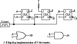
D flip-flops: 3 gates, 5 literals, 9 wires (Figure 7.36) 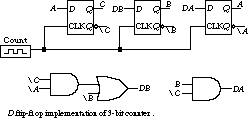
Although it is difficult to generalize from a single example, J-K flip-flops usually yield the most gate- and literal-efficient implementations. Since the R-S flip-flop behavior is a proper subset of a J-K, there is never any advantage in using R-S devices as counter storage elements. In fact, you would be hard pressed to find them in the usual parts catalogs (although R-S latches are readily available).
T flip-flops are well suited for implementing straightforward binary counters, but their advantage is mitigated when the counter must follow a sequence that is not in direct binary order. In the example of this section, the T flip-flop implementation was worst by a wide margin.
Although they do not often yield the most gate-efficient solution, D flip-flops have some important advantages. First, they simplify the design procedure, allowing you to skip the next-state remapping step. Tools like espresso and misII can be applied to the state transition table, treated as a truth table, to obtain a minimized implementation rapidly.
Second, if wiring complexity rather than gate count dominates the design, D flip-flops usually have the advantage (in our example, the D and J-K implementations had the same wiring complexity). Only a single input must be routed to a D flip-flop, compared to two inputs in the case of a J-K storage element.
Wiring complexity is especially important when using programmable logic technologies. Often the number of functional outputs supported by a programmable logic part is more constrained than the complexity of the logic that can be implemented, such as the number of product terms.
Finally, D storage elements are particularly transistor efficient in MOS VLSI technologies, as we saw in Chapter 6. J-K flip-flops require many more transistors for their implementation.
To summarize, for conventional packaged MSI/SSI TTL design, J-K flip-flops are usually preferable, especially when the design criterion is minimum gate and literal count. D-type devices are preferred when designing with programmable logic or in technologies more highly integrated than TTL, where minimum wire count or a simplified design procedure is the goal.
[Top] [Next] [Prev]