25.
1. (State Reduction) Verify that the code converter problem statement of Section 10.1.2 yields the reduced state transition table and state diagram of Figures 10.3 and 10.4. Start with a general state diagram derived directly from the problem statement, and show how it is reduced. 2.
(Reset in Finite State Machines) Consider the BCD-to-Excess-3 code converter state machine. In various implementations of this machine, reset was used to control the state register's clear signal directly. How does the next-state logic change when reset is treated as an explicit input, for the following implementations: The ROM-based approach of Figures 10.5 and 10.6
A PLA-based approach as suggested by Figures 10.9 and 10.11
3.
(Actel Logic Module) Figure 10.32 showed the basic Actel logic module. Show how a single logic module can be used to implement the following functions: A two-input AND gate4.
A two-input NAND gate
A two-input NOR gate with one input inverted
A two-input XOR gate
The logic function Y=(A B)+C
The logic function Y=(A+B)C
The logic function Y=(A B)+(A C)+(B C). This function is also known as the majority function.
(Actel Logic Module) Describe how to implement the following functions using two Actel logic modules: A four-input AND-OR-Invert structure with two 2-input AND gates at the first level
Y=
+
+C+D
5.
(Actel Logic Module) Show how to implement a half adder in terms of an Actel logic module (more than one module may be needed). How would you implement the full adder circuit? (Hint: This can be done in two logic modules if the carry-in and carry-out are designed to be active low.)6.
(Actel Logic Module) Figure 10.33 showed how to implement an 7.
(Xilinx CLB) The function generator within the Xilinx CLB can implement any combinational logic function of five inputs. This is equivalent to how many two-input gates? Explain how you derived your answer.8.
(Xilinx CLB) A single Xilinx CLB can implement a five-input parity function. Show how a two-level CLB structure can implement a 25-input parity function.9.
How many input parity functions can be implemented by a three-level CLB structure?
(Xilinx CLB) The Xilinx CLB can implement any single combinational logic function F(A,B,C,D,E) of five variables OR two independent functions F(A,B,C,D) and G(A,B,C,D) of four (or less) variables. Show how this might be implemented by wiring up a 32-input function generator10.(multiplexer/selector)using two 16-to-1 and three 2-to-1 multiplexers. Assume that input0 is selected when EABCD=00000, input15 when EABCD=01111, input16 when EABCD=10000, and input31 when EABCD=11111. Besides the five data inputs A, B, C, D, and E, there is a control input M such that when M=0 the function generator generates the two independent four-variable functions F and G, and when M=1 it generates the single five-variable function on both the F and G outputs.
What must the input settings be to implement the five-variable function F=A Ý B Ý C Ý D Ý E?
What must the input settings be to implement the two 3--variable functions F(A,B,C)=A Ý B Ý C(full adder sum)and G(A,B,C)=AB+BC+AC(full adder carry)?
(Traffic Light Controller) The description of the traffic light con-troller in Section 10.4.1 assumes that the traffic light outputs from the state machine are encoded. This saves only two output lines, yet introduces the extra complexity (and parts count) of -external -decoders. Rederive the equations for the traffic light control signals, assuming fully decoded outputs from the state machine: HG, HY, HR, FG, FY, FR. Also show the revised state transition table.11.
How does this affect the PAL-based implementation? In -particular, will you require a PAL with more product terms per output or fewer terms per output?
How does the change affect the ROM-based implementation?
(Traffic Light Controller) The traffic light controller as presented in Section 10.4.1 is a Mealy machine. Modify the description to make it part Moore/part Mealy by decoding the traffic light control signals directly from the state, as we did in Section 10.4.3. What are the implications for a PAL-based implementation?
How does this affect the ROM-based implementation?
12.
(Traffic Light Controller) The end of Section 10.4.4 described how to implement the traffic light controller finite state machine in terms of MSI-style components mapped onto Xilinx CLBs. -Verify that the ST function can be implemented by a single CLB by giving the truth table for the five-variable function ST(TL, TS, C, Q1, Q0).13.
(Implementing Finite State Machines) Follow the complete implementation process for the string recognizer finite state machine from Section 8.5.1. Choose a state assignment and determine the minimized next-state and output functions. Given the equations you derived for the next-state and output functions, determine the kind of PAL you will need to complete the implementation. Consider such factors as number of inputs, number of registered versus combinational outputs, and number of product terms per output.
Repeat the analysis for Xilinx LCAs. How many CLBs will you need to realize the set of equations you derived?
14.
(Implementing Finite State Machines) Repeat Exercise 10.13, but for the complex counter finite state machine of Section 8.5.2. 15.
(Implementing Finite State Machines) Repeat Exercise 10.13, but this time for the 3-bit combination lock of Section 8.5.4.16.
(Implementing Finite State Machines) Repeat Exercise 10.13, but for the reduced state diagram of the 3-bit string recognizer of -Figure 9.27. Use one of the good state assignments of Figure 9.28. What are the implications of choosing a state assignment in which the start state is not encoded as 0?17.
(Implementing Finite State Machines) Repeat Exercise 10.13, but for the reduced state diagram of the 4-bit string recognizer of -Figure 9.7. Use one of the good state assignments from Figure 9.29.18.
(Implementing Finite State Machines) Repeat Exercise 10.13, but for the reduced multi-input state diagram of Figure 9.17. Use a straightforward state assignment: S0' = 00, S1 = 01, S2 = 10, S3' = 11.19.
(Implementing Finite State Machines) Implement an 8-bit register using the 20X10 PAL of Figure 10.16 to the following specifications:The register has three control inputs,
(output enable), (load), and CLK (clock), and eight data inputs D7-D0. It has eight registered outputs Q7-Q0. When the outputs are in high impedance. When
The register has three control inputs:
(output enable), CLR/(clear/increment), and CLK (clock), and eight data outputs, Q7-Q0. When (Hint: consider the carry look-ahead logic described in Chapter 5, except simplified for the specific case where the sum is A + 1.)
20.
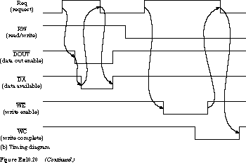
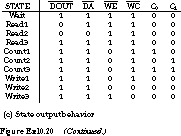
(Implementing Finite State Machines) In this exercise, you will design a memory controller finite state machine that implements a processor-memory handshake to the following specification. The processor initiates a transfer request by asserting REQ (request) while specifying a read or write (RW) operation. During a read operation (RW asserted), the processor waits for the memory controller to assert (data available). The processor can then sample the data. It unasserts the REQ line to end the memory cycle. During a write operation (RW unasserted), the processor drives data to the memory system, waiting for the memory controller to assert (write complete). When the processor sees this, it unasserts REQ to end the cycle. This is a variation of the four-cycle handshake described in Chapter 4.The Moore state diagram for the memory controller is shown in Figure Ex10.20
(a). Note that the read and write require multiple states for their execution. A timing diagram, showing the -relationships between the critical control signals for a read and a write cycle, is given in Figure Ex10.20(b). The state control signal -outputs are listed in Figure Ex10.20(c). Several of the memory controller's signals listed here are used to control the memory components. Their detailed meaning is not important, except that the appropriate signals should be asserted in the listed states. 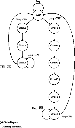
Choose a good state assignment and implement using discrete gates and D flip-flops. What kind of PAL would you need to implement this machine in a single chip (in particular, -number of inputs/outputs, flip-flops, product terms per output, etc.)?
How many Xilinx CLBs would it take to implement your solution to part (a)? Justify your answer.
Implement the state machine using a four-bit counter as a state register. Show your counter-based state assignment, and your implementation of the next state function in terms of clear, count, and load. What kind of PAL would you need to implement the next state control in a single chip (assume the state register is implemented externally with a 74163 synchronous up-counter)?
How many Xilinx CLBs would it take to implement your solution to part (c), including the counter state register and the output logic?
[Top] [Next] [Prev]