Eighth-Generation (64-Bit Register) Processors
| As of 2001, it had been about 15 years since PCs had begun to support 32-bit processors (all processors from the 80386 up through the Intel Pentium 4 and AMD Athlon XP). However, in 2001, Intel introduced the first 64-bit processor for serversthe Itaniumfollowed in 2002 by the improved Itanium 2. In 2003, AMD introduced the first 64-bit processor for x86-compatible desktop computersthe Athlon 64followed by its first 64-bit server processor, the Opteron. In 2004, Intel introduced a series of 64-bitenabled versions of its Pentium 4 desktop processor. Then in 2005, Intel introduced 64-bit versions of its Xeon workstation and server processors and new 64-bit desktop processorsthe Pentium Extreme Edition and dual-core Pentium D. The following sections discuss the major features of these processors and the different approaches taken by Intel and AMD to bring 64-bit computing to the PC server and desktop. Intel Itanium and Itanium 2Introduced on May 29, 2001, the Itanium was the first processor in Intel's IA-64 (Intel Architecture 64-bit) product family, and it incorporated innovative performance-enhancing architecture techniques, such as prediction and speculation. It and its newer sibling, the Itanium 2 (introduced in June 2002), are the highest-end processors from Intel and are designed mainly for the server market. If Intel was still using numbers to designate its processors, the Itanium family might be called the 886 because the Itanium and Itanium 2 are the eighth-generation processors in the Intel family, and they represent the most significant processor architecture advancement since the 386. Intel's IA-64 product family is designed to expand the capabilities of the Intel architecture to address the high-performance server and workstation market segments. The Itanium and Itanium 2 were never designed to replace the Pentium 4. They feature an all-new design that is initially expensive and is found only in the highest-end systems such as file servers or advanced workstations. The Itanium's technical details are listed in Table 3.48.
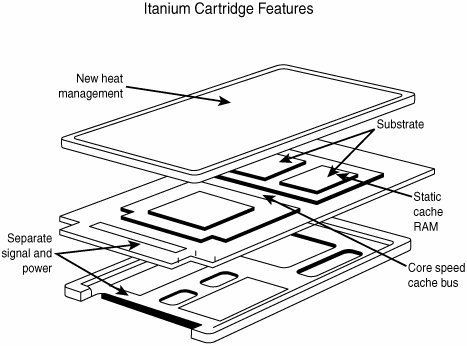
As noted in Table 3.48, the Itanium and Itanium 2 are the first Intel processors with three levels of integrated cache. Even though a few previous system designs featured L3 cache, the L3 cache was located on the motherboard and was therefore much slower. By building L3 cache in to the cartridge (Itanium) or on the processor die (Itanium 2), all three cache levels run at the full processor speed. The following features apply to both Itanium and Itanium 2 processors:
The Itanium 2 also features
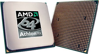
Itanium and Itanium 2 were initially based on 0.18-micron technology; however, current versions of the Itanium 2 are based on 0.13-micron, allowing for higher speeds and larger caches. The original Itanium used a cartridge known as the pin array cartridge (PAC). This cartridge includes L3 cache and plugs into a PAC418 (418-pin for Itanium) or PAC611 (611-pin for Itanium 2) socket on the motherboard and not a slot. The package is about the size of a standard index card, weighs about 6oz. (170g), and has an alloy metal on its base to dissipate the heat (see Figure 3.62). Itanium has clips on its sides, enabling four of them to be hung from a motherboard, both below and above. Figure 3.62. The Itanium's pin array cartridge. The first Itanium 2 was codenamed McKinley and officially introduced in June 2002. The current version uses the 0.13-micron Madison core, which has up to a whopping 592 million transistors in its 9MB on-die L3 cache version. Because the Itanium 2 has a significantly higher CPU bus bandwidth (up to 10.6GBps), higher clock speeds, larger caches, and a processor FSB twice as wide (128 bits) as the original Itanium, the Itanium 2 is significantly faster in overall processing. The Itanium 2 integrates all three levels of cache inside the processor die, so a cartridge is unnecessary (see Figure 3.63). The Itanium and Itanium 2 are not interchangeable and are supported by different sockets and chipsets. Figure 3.63. The Itanium 2 is a more compact design than the original Itanium. Photograph used by permission of Intel Corporation. The Itanium and Itanium 2 are supported by a variety of operating systems, including Microsoft Windows (XP 64-bit Edition and 64-bit Windows Advanced Server Limited Edition 2002), Linux (from four distributor companies: Red Hat, SuSE, Caldera, and Turbo Linux), and two Unix versions (Hewlett-Packard's HP-UX and IBM's AIX). Tip If you need to run 32-bit x86 software on an Itanium 2 processor, be sure your OS supports the IA-32 Execution Layer (IA-32 EL) technology. IA-32 EL improves the performance of 32-bit software on the Itanium 2 processor. Operating systems that include or support IA-32 EL include Windows Server 2003 Enterprise Edition, Windows Server 2003 Data Center, Windows XP 64-bit Edition, and most current Linux distros that support Itanium 2. You can download IA-32 EL for Red Hat Enterprise Linux 4; Red Hat Enterprise Linux 3 UP5; Red Hat Enterprise 3 UP4; SUSE Enterprise Server 9 SP1; SUSE Enterprise Server Linux SP1, Kernel 2.6 from the "IA-32 Execution Layer" page at http://www.intel.com/cd/software/products/asmo-na/eng/219773.htm. Although Itanium 2 has broad OS support, it has not proven to be as popular as Intel and hardware vendors initially hoped. Although Intel continues to develop new versions of the Itanium 2 platform, it's more likely that your first foray into 64-bit computing will use one of the AMD or Intel processors discussed in the following sections. That's because other 64-bit processors natively use extensions of the existing IA-32 architecture for full-speed 32-bit and 64-bit computing and cost little more (if anything) than comparable 32-bitonly processors. AMD Athlon 64 and 64 FXThe AMD Athlon 64 and 64 FX, introduced in September 2003, are the first 64-bit processors for desktop (and not server) computers. Originally code named ClawHammer, the Athlon 64 and 64 FX are the desktop element of AMD's 64-bit processor family, which also includes the Opteron (code named SledgeHammer) server processor. The Athlon 64 and 64 FX (shown in Figure 3.64) are essentially Opteron chips but are designed for single-processor systems, and in some cases have decreased cache or memory bandwidth capabilities. Figure 3.64. AMD Athlon 64 FX (Socket 939 version). Photo courtesy of AMD. Besides support for 64-bit instructions, the biggest difference between the Athlon 64 and 64 FX and other processors is the fact that their memory controller is built in. The memory controller is normally part of the motherboard chipset North Bridge or memory controller hub (MCH) chip, but with the Athlon 64 and 64 FX, the memory controller is now built in to the processor. This means that the typical CPU bus architecture is different with these chips. In a conventional design, the processor talks to the chipset North Bridge, which then talks to the memory and all other components in the system. Because the Athlon 64 and 64 FX have integrated memory controllers, they talk to memory directly, and also talk to the North Bridge for other system communications. Separating the memory traffic from the CPU bus allows for greatly improved performance not only in memory transfers, but also in CPU bus transfers. The main difference in the Athlon 64 and 64 FX is in the different configurations of cache sizes and memory bus widths. The major features of the Athlon 64 design include
The Athlon 64 FX differs from the standard Athlon 64 in the following ways:
Although Socket 939 versions of the Athlon 64 have closed the performance gap, the Athlon 64 FX is still the fastest single-core Athlon 64 processor. Although AMD has been criticized by many, including me, for its confusing performance-rating processor names in the Athlon XP series, AMD also uses this naming scheme with the Athlon 64. As I suggest with the Athlon XP, you should look at the actual performance of the processor with the applications you use most to determine whether the Athlon 64 is right for you and which model is best suited to your needs. The integrated memory bus in the Athlon 64 means that the Athlon 64 connects to memory more directly than any 32-bit chip and makes North Bridge design simpler. AMD offers its own chipsets for the Athlon 64, but most Athlon 64 motherboards and systems use third-party chipsets from the same vendors that now produce Athlon XP chipsets. See Chapter 4 for details. The various models and features of the Athlon 64 and 64 FX are summed up in Tables 3.49 and 3.50.
The Athlon 64 and 64 FX are available in three socket versions (see Table 3.51). The Athlon 64 is available in Socket 754 and Socket 939 versions, whereas the 64 FX is available in Socket 939 and Socket 940 versions. Socket 754 supports only a single-channel memory bus, whereas Sockets 939 and 940 both support dual-channel memory for double the memory bandwidth. Socket 939 also supports faster and cheaper unbuffered DDR SDRAM DIMMs; Socket 940 supports slower and more expensive registered DIMMs. Because of this, you should avoid any Socket 940 processors or motherboards because they require registered modules that are both slower and more expensive than unbuffered types. Socket 754 versions of the Athlon 64 are also designed to use more affordable unbuffered modules, but only in single-channel mode.
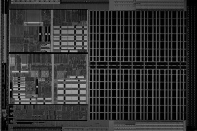
The Athlon 64 essentially comes in two versions: a Socket 754 version that has only a single-channel memory bus and an improved Socket 939 version that has a dual-channel memory bus. The Athlon 64 FX is also available in two versions: a Socket 940 version that uses expensive (and slower) registered memory and an improved Socket 939 version that uses unbuffered memory. The Socket 939 versions of the Athlon 64 and 64 FX are essentially the same chip, differing only in the amount of L2 cache included. For example, the Athlon 64 3800+ and Athlon 64 FX-53 both run at 2.4GHz and run dual-channel memory. The only difference is that the 3800+ has only 512KB of L2 cache whereas the FX-53 has 1MB of L2. Because the 64 and 64 FX chips are essentially the same, you need to read the fine print to determine the minor differences in configuration. The Athlon 64 and 64 FX can draw up to 104W or more of power, which is high but still somewhat less than the more power-hungry Pentium 4 processors. As with the Pentium 4, motherboards for the Athlon 64 and 64 FX require the ATX12V connector to provide adequate 12V power to run the processor voltage regulator module. The initial version of the Athlon 64 is built on a 0.13-micron (130-nanometer) process (see Figure 3.65). Subsequent versions use a 0.09-micron (90-nanometer) process. Figure 3.65. AMD Athlon 64 die (130-nanometer process, 106 million transistors, 193 sq. mm). Photo courtesy of AMD. AMD Sempron (Socket 754)Just as the Intel Celeron name long ago ceased to identify a particular processor and instead is a brand used by Intel to identify various types of low-cost, reduced-performance processors, AMD's Sempron brand follows a similar course. Sempron is used to identify both Socket A processors that have replaced the Athlon XP and Socket 754 processors that provide a low-cost alternative to the Athlon 64.
The Socket 754 Sempron is based on the Socket 754 version of the Athlon 64 processor. However, some versions of the Sempron operate only in a 32-bit mode. The major features of the Socket 754 Sempron include
A system using a Socket 754 Sempron processor can be easily upgraded to a Socket 754 Athlon 64 processor. Table 3.52 provides detailed information about Socket 754 Sempron processors. As Table 3.52 indicates, most Socket 754 Sempron models support AMD64 64-bit computing. With both Intel and AMD offering entry-level 64-bit processors, it's easier than ever to move into 64-bit computing. AMD OpteronThe AMD Opteron is the workstation and server counterpart to the AMD Athlon 64, supporting the same AMD64 (x86-64) architecture as the Athlon 64. The Opteron was introduced in the spring of 2003. The following are the major features of the Opteron:
The Opteron is available in three series: 100 (single-processor workstations), 200 (dual-processor workstations and servers), and 800 (up to eight-way servers). Dual-core versions of Opteron processors are available in all three of these series. Unlike the Itanium series, which has been supported primarily by Intel chipsets, the Opteron has broad third-party chipset support from companies such as VIA, SiS, ULi, NVIDIA, and ATI (just like the Athlon 64 does). For more information on Opteron configurations and features, see the book Upgrading and Repairing Servers. |
EAN: 2147483647
Pages: 283