Memory Types
| Over the years , four main types of memory have been used in PCs:
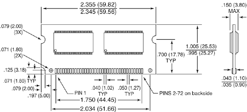
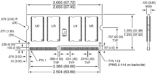
All of these, except the RDRAM, have been used in laptops and other portable systems. The following sections discuss each of these memory types in more detail. Fast Page Mode DRAMStandard DRAM is accessed through a technique called paging . Normal memory access requires that a row and column address be selected, which takes time. Paging enables faster access to all the data within a given row of memory by keeping the row address the same and changing only the column. Memory that uses this technique is called Page Mode or Fast Page Mode memory. Other variations on Page Mode were called Static Column or Nibble Mode memory. Most Intel 486 as well as AMD or Cyrix 5x86-based laptops from the mid-1990s and earlier used FPM memory. Paged memory is a simple scheme for improving memory performance that divides memory into pages ranging from 512 bytes to a few kilobytes long. The paging circuitry then enables memory locations in a page to be accessed with fewer wait states (idle or do-nothing cycles). If the desired memory location is outside the current page, one or more wait states are added while the system selects the new page. To improve further on memory access speeds, systems have evolved to enable faster access to DRAM. One important change was the implementation of burst mode access in the 486 and later processors. Burst mode cycling takes advantage of the consecutive nature of most memory accesses. After setting up the row and column addresses for a given access, using burst mode, you can then access the next three adjacent addresses with no additional latency or wait states. A burst access usually is limited to four total accesses . To describe this, we often refer to the timing in the number of cycles for each access. A typical burst mode access of standard DRAM is expressed as x-y-y-y; x is the time for the first access (latency plus cycle time), and y represents the number of cycles required for each consecutive access. Standard 60ns DRAM normally runs 5-3-3-3 burst mode timing. This means the first access takes a total of five cycles (on a 66MHz bus, this is about 75ns total or 5 x 15ns cycles), and the consecutive cycles take three cycles each (3 x 15ns = 45ns). As you can see, the actual system timing is somewhat less than the memory is technically rated for. Without the bursting technique, memory access would be 5-5-5-5 because the full latency is necessary for each memory transfer. For laptop systems, FPM RAM generally came in 72-pin or 144-pin EDO SO-DIMM (small outline dual inline memory module) form. Figures 6.1 and 6.2 (later in this chapter) show the physical characteristics of these 72-pin and 144-pin SO-DIMMs. These modules normally operate on 3.3V, saving power as compared to their full- sized 5V counterparts for desktop systems. Figure 6.1. 72-pin SO-DIMM. Figure 6.2. 144-pin SO-DIMM. Extended Data Out RAMIn 1995, a newer type of memory called extended data out ( EDO ) RAM became available for Pentium systems. EDO, a modified form of FPM memory, is sometimes referred to as Hyper Page mode . EDO was invented and patented by Micron Technology, although Micron then licensed production to many other memory manufacturers. EDO memory consists of specially manufactured chips that allow a timing overlap between successive accesses. The name extended data out refers specifically to the fact that unlike FPM, the data output drivers on the chip are not turned off when the memory controller removes the column address to begin the next cycle. This enables the next cycle to overlap the previous one, saving approximately 10ns per cycle. The effect of EDO is that cycle times are improved by enabling the memory controller to begin a new column address instruction while it is reading data at the current address. This is almost identical to what was achieved in older systems by interleaving banks of memory. Unlike interleaving, however, EDO doesn't require that you install two identical banks of memory in the system. EDO RAM allows for burst mode cycling of 5-2-2-2, compared to the 5-3-3-3 of standard Fast Page Mode memory. To do four memory transfers, then, EDO would require 11 total system cycles, compared to 14 total cycles for FPM. This is a 22% improvement in overall cycling time, but in actual testing, EDO typically increases overall system benchmark speed by only about 5%. Even though the overall system improvement might seem small, the important thing about EDO was that it used the same basic DRAM chip design as FPM, meaning that there was practically no additional cost over FPM. In fact, in its heyday, EDO cost less than FPM and yet offered higher performance. For laptop systems, EDO RAM generally came in 72-pin or 144-pin EDO SO-DIMM (small outline dual inline memory module) form. Figure 6.1 and 6.2 (later in this chapter) shows the physical characteristics of these 72-pin and 144-pin SO-DIMMs. These modules normally operate on 3.3V, saving power as compared to their full-sized 5V counterparts for desktop systems. To actually use EDO memory, your motherboard chipset must support it. Most laptop motherboard chipsets ”starting in 1995 with the Intel 430MX (Mobile Triton) and through 1997 with the 430TX ”offered support for EDO. Because EDO memory chips cost the same to manufacture as standard chips, combined with Intel's support of EDO in all its chipsets, the PC market jumped on the EDO bandwagon full force. EDO RAM was ideal for systems with bus speeds of up to 66MHz, which fit perfectly with the PC market up through 1997 and into 1998. However, since 1998, the market for EDO rapidly declined as the newer and faster SDRAM architecture has become the standard for new PC and laptop system memory. SDRAMSDRAM is short for synchronous DRAM , a type of DRAM that runs in synchronization with the memory bus. SDRAM delivers information in very high-speed bursts using a high-speed, clocked interface. SDRAM removes most of the latency involved in asynchronous DRAM because the signals are already in synchronization with the motherboard clock. As with EDO RAM, your chipset must support this type of memory for it to be usable in your system. Starting in 1997 with the 430VX and 430TX (only the TX was used in mobile systems), most of Intel's chipsets began to support industry standard SDRAM, making it the most popular type of memory for new systems through 2000 and even into 2001. SDRAM performance is a dramatic improvement over FPM and EDO RAM. Because SDRAM is still a type of DRAM, the initial latency is the same, but overall cycle times are much faster than with FPM or EDO. SDRAM timing for a burst access would be 5-1-1-1, meaning that four memory reads would complete in only eight system bus cycles, compared to 11 cycles for EDO and 14 cycles for FPM. This makes SDRAM almost 20% faster than EDO. Besides being capable of working in fewer cycles, SDRAM is also capable of supporting up to 133MHz (7.5ns) system bus cycling. As such, most new PC systems sold from 1998 to 2000 have included SDRAM memory. For laptop and portable systems, SDRAM is sold in 144-pin SO-DIMM or Micro-DIMM form. It is often rated by both megahertz speed and nanosecond cycling time, which can be kind of confusing. Figure 6.2 (later in this chapter) shows the physical characteristics of 144-pin SDRAM SO-DIMMs and 144-pin SDRAM Micro-DIMMs. Like their full-sized DIMM desktop counterparts, the SO-DIMMs use 3.3V power. To meet the stringent timing demands of its chipsets, Intel created specifications for SDRAM called PC66, PC100, and PC133. To meet the PC100 specification, 8ns chips usually are required. Normally, you would think 10ns would be considered the proper rating for 100MHz operation, but the PC100 specification calls for faster memory to ensure all timing parameters are met. In May of 1999, JEDEC created a specification called PC133. It achieved this 33MHz speed increase by taking the PC100 specification and tightening up the timing and capacitance parameters. The faster PC133 quickly caught on as the most popular version of SDRAM for any systems running a 133MHz processor bus. The original chips used in PC133 modules were rated for exactly 7.5ns or 133MHz, whereas later ones were rated at 7.0ns or 143MHz. These faster chips were still used on PC133 modules, but they allowed for improvements in column address strobe latency (abbreviated as CAS or CL ), which improves overall memory cycling times somewhat. Table 6.4 shows the timing, actual speed, and rated speed for various SDRAM DIMMs. Table 6.4. SDRAM Timing, Actual Speed, and Rated Speed
DDR SDRAMDouble data rate ( DDR ) SDRAM memory is an evolutionary design of standard SDRAM in which data is transferred twice as quickly. Instead of doubling the actual clock rate, DDR memory achieves the doubling in performance by transferring data twice per transfer cycle: once at the leading (falling) edge and once at the trailing ( rising ) edge of the cycle. This is similar to the way RDRAM operates and effectively doubles the transfer rate, even though the same overall clock and timing signals are used. DDR found most of its initial support in the graphics card market; since then it has become the mainstream PC memory standard for both desktop and portable systems. DDR SDRAM came to market during 2000, but it didn't really catch on in the portable market until the advent of the Intel 845MP chipset in March 2002. For laptop and portable systems, DDR SDRAM uses either 200-pin SO-DIMMs or 172-pin Micro-DIMMs. Figures 6.1 and 6.2 (later in this chapter) show both types of modules, respectively. DDR SO-DIMMs come in a variety of speed or throughput ratings and normally run on 2.5 volts , just like their full-sized desktop counterparts. They are basically an extension of the standard SDRAM SO-DIMMs redesigned to support double clocking, where data is sent on each clock transition (twice per cycle) rather than once per cycle, as with standard SDRAM. To eliminate confusion with DDR, regular SDRAM is often called single data rate (SDR) . Table 6.5 compares the different types of standard SDRAM and DDR SDRAM SO-DIMM modules available. Table 6.5. SDRAM and DDR SDRAM Module Types and Bandwidth
Note that several of these specifications either don't exist yet or could exist but haven't been developed into products. Currently the fastest standardized modules are PC3200. Faster modules don't exist yet, but faster modules are always being developed. Even faster technologies such as DDR are on the horizon. DDR2 SDRAMJEDEC and its members have been working on the DDR2 specification for several years now, and the specification is finally coming to fruition. Although DDR2 chips and modules will be appearing for desktop systems in 2004, it may take a while longer for them to reach laptops or other portable systems. DDR2 SDRAM is simply a faster version of conventional DDR-SDRAM memory. It achieves higher throughput by using differential pairs of signal wires to allow faster signaling without noise and interference problems. The original DDR specification tops out at 400MHz to 533MHz, whereas DDR2 starts at 400MHz and will go up to 800MHz and beyond. In addition to providing greater speeds and bandwidth, DDR2 has other advantages. It uses lower voltage than conventional DDR (1.8V versus 2.5V), so power consumption and heat generation are reduced. Because of the greater number of pins required on DDR2 chips, the chips normally use FBGA (fine-pitch ball grid array) packaging rather than the TSOP (thin small outline package) chip packaging used by most DDR and conventional SDRAM chips. FPGA chips are connected to the substrate (meaning the memory module in most cases) via tightly spaced solder balls on the base of the chip. RDRAMRambus DRAM ( RDRAM ) is a fairly radical memory design found in high-end Pentium 4 “based desktop PC systems starting in late 1999. Intel signed a contract with Rambus in 1996 ensuring it would support RDRAM into 2001. That period has elapsed, and Intel has abandoned RDRAM support for future chipsets beyond that date, even though RDRAM standards have been proposed that will support processors through 2006. Because there never were any RDRAM supporting chipsets for laptop or notebook systems, you normally don't see RDRAM associated with portables. For more information on RDRAM, see the RDRAM section in the "Memory" chapter of my book Upgrading and Repairing PCs . | ||||||||||||||||||||||||||||||||||||||||||||||||||||||||||||||||||||||||||||||||||||||||||||||||||||||||||||||||||||||||||||||||||||||||||||||||||||||||||||||||||||||||||||||||||||||||||||||||||
EAN: 2147483647
Pages: 182